Week08. Electronics Production
1. Assignment and Result
About the process, I made new page and made links are below, because the long page makes me confuse.
| GROUP ASSIGNMENT | THE RESULT |
|---|---|
| - characterize the design rules for your in-house PCB production process | Process -> Kitakagaya: Week8 Electronics Production 1. Board Design (2D data) 2. Create tool Path (MODS) 3. Milling (MDX-40A, using VPanel) |
| - extra credit: make it with another process | |
| - extra credit: send a PCB out to a board house |
| INDIVIDUAL ASSIGNMENT | THE RESULT |
|---|---|
| - make and test the development board that you designed to interact and communicate with an embedded microcontroller |
PROCESS -> ATtiny414 Board with LED and Switch 1. Design board with Kicad. 2. Create tool Path (V Carve Pro) 3. Milling (MDX-40A, using VPanel) 4. Soldering 5. Programming (Arduino IDE, and ChatGPT) |
| - extra credit: make it with another process | - |
2. HERO SHOT
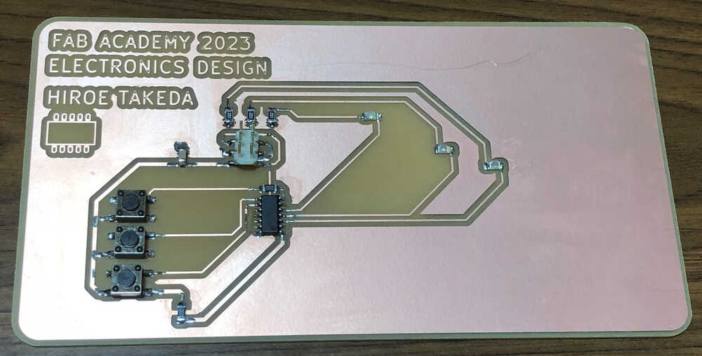
My original Board
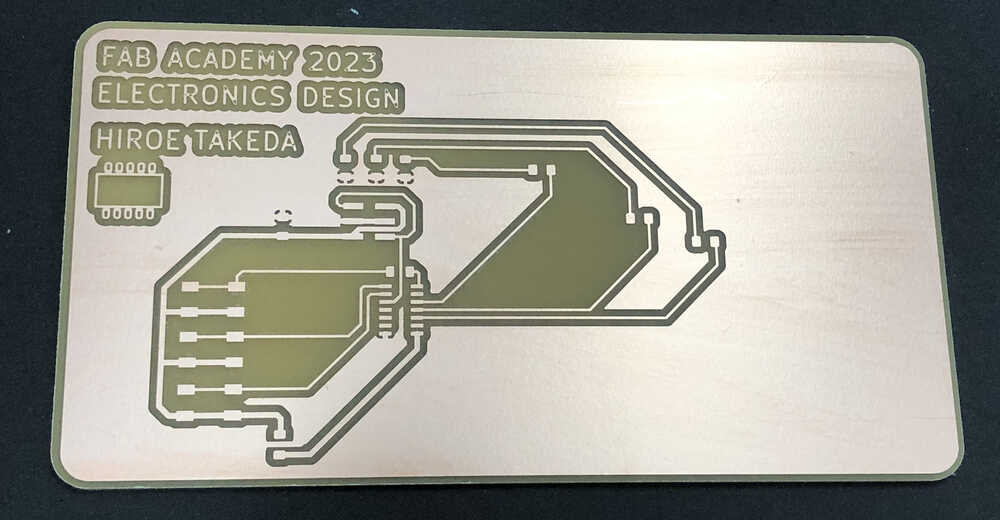
My original development board with ATtiny414, with LED and Pushbutton switch.
3. The Video
I put the map on the board. The map is for Kinki region in Japan, and the LED is location of FabLab West-harima, FabLab Kobe, and FabLab Kitakagaya. The each LED blink with each pushbutton switch, as below Video shows.
4. Main Flow of Electronics Production
- select chip & parts and check datasheet
- Board Design
- Create tool Path
- Milling
- Soldering
- Programming
5. My Thought
- The first time I cut a board in pre-study, it took a long time and try a lot. During pre-study, need to mill so many hours, as the mill is not reached to board. One time, the mill flute is broken, as I made the mistake the wrong origin.
- I think I was able to cut the substrate well because I have practiced many times before and took on this week's challenge.
- Creating a board is very time consuming, about design board, and Soldering, and tester and programming.
- Soldering small electronic components is extremely difficult. Soldering small parts (especially ATtiny414 and FT230) leg by leg was quite difficult. I realized my old eyesight for the first time with this solder. I thought it would have been easier if I had taken FabAcademy when I was younger.
- During the soldering process, we checked many times to make sure the orientation of electronic components is correct.
- We learned in advance to use Kicad and to solder, which was good. Otherwise, I would have cried by now.