- Kicad (Process)
For the individual assignment, I used Kicad for the Electronics Design.
I draw the prototype of Main board of my final Project. The process is below.
1.The Setup
1-1) Install Kicad
- I installed "Kicad 6.0" from Kicad Website , as my pre-study.
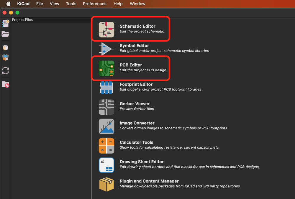
- In Kicad,
- Schematic is for the schematic design (symbol,footprint, and how wire).
- PCB is for PCB design (layout).
1-2) Library
Add Library (symbol and Footprint) is useful, the process is below.
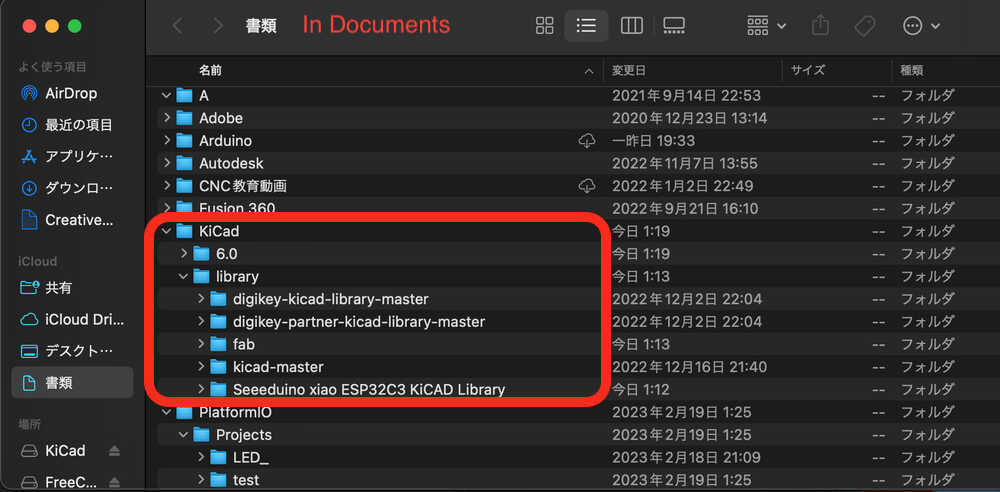
- I download the below Kicad LIBRARY.
- In Documents > KiCad > 6.0 > Libraries (I created this folder) > download libraries (store download libraries here)
- Open KiCad
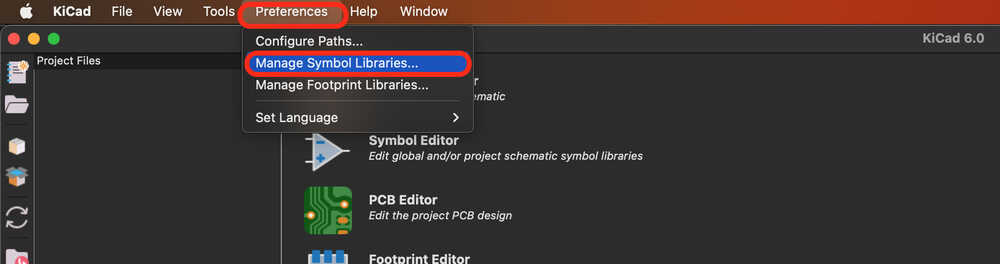
- Preference > Manage Symbol Libraries
- click "+ button", and Press folder icon in Library Path and select "fab.kicad_sym" file, then click OK.
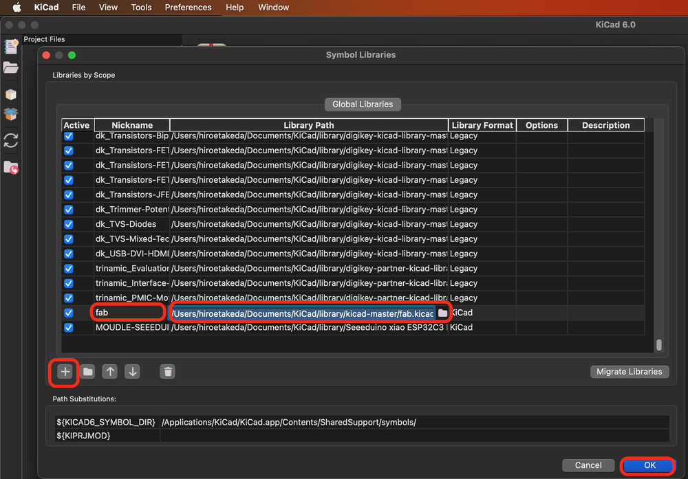
- click "+ button", and Press folder icon in Library Path and select "fab.kicad_sym" file, then click OK.
- Preference > Manage Footprint Libraries.
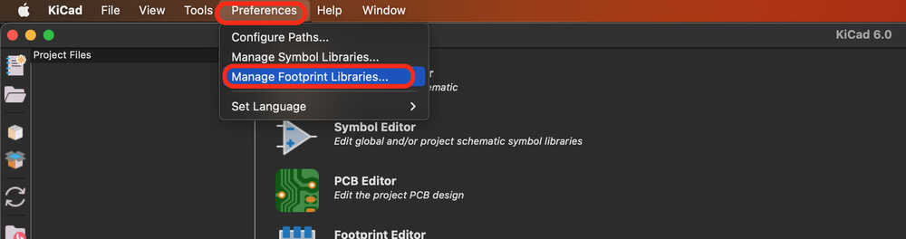
- click "+ button" , and Press folder icon in Library Path and select "fab.pretty"folder, then click OK.
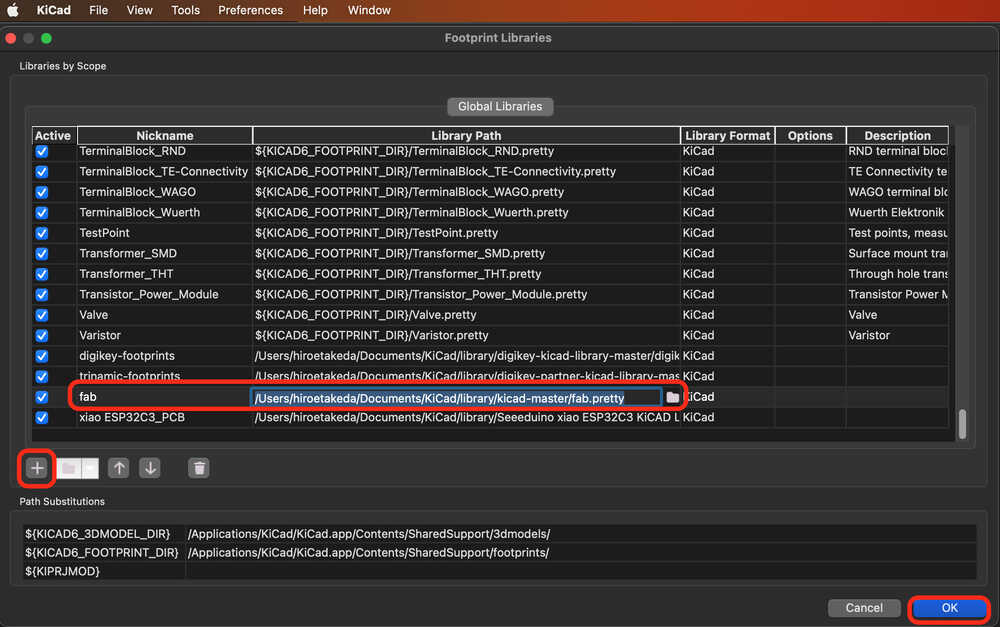
- click "+ button" , and Press folder icon in Library Path and select "fab.pretty"folder, then click OK.
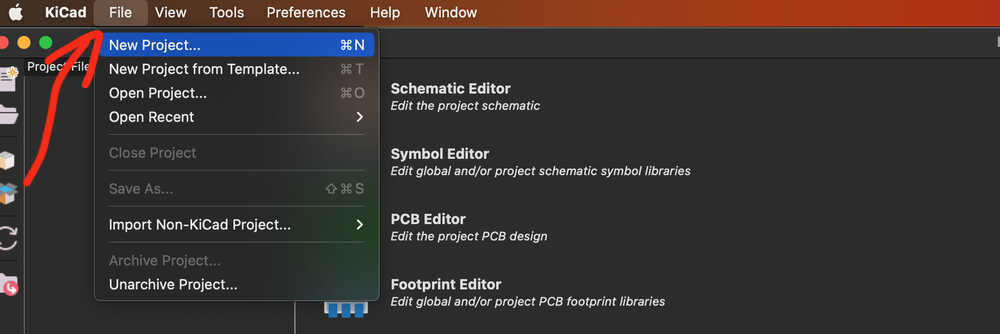
2. Create New Project
Create New Project of prototype main board for my final Project. The process is below.
- File > New Project
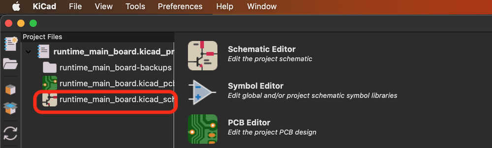
3. Schematic
- Open Schematic Editor.
- In Schematic editor, I mainly use the bottom below with mark.
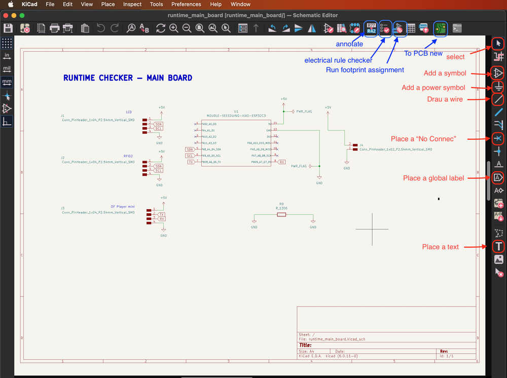
3-1) Symbol
- Click "Add a Symbol" in the right bar menu.
- Enter the text, and search, then click the item to use, and click OK.
- Rotate symbols with R key, if needed.
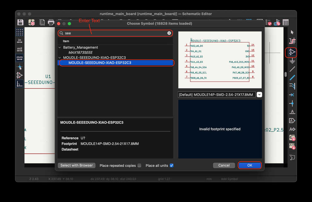
- Add other Symbol as same process.
- About pin header, I wanted added a pin header that is a different type, but there isn't it in the symbol. So I chose the other pin header is same pitch and same footprint.
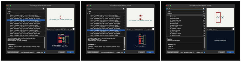
- About pin header, I wanted added a pin header that is a different type, but there isn't it in the symbol. So I chose the other pin header is same pitch and same footprint.
3-2) Power Symbol
Add a power Symbol in the right bar menu (e.g.GND, +5V, +3V3).
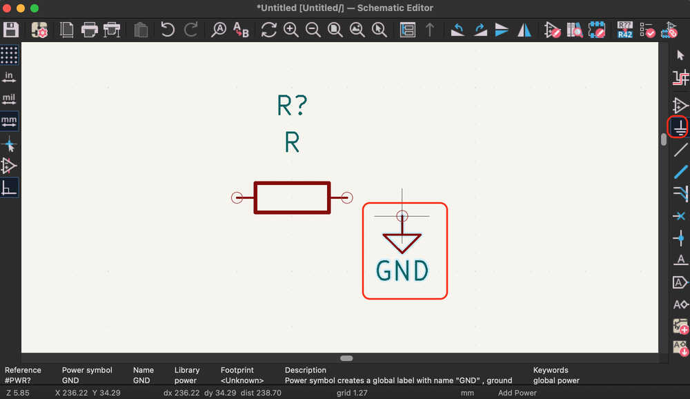
- Click add wire button in the right bar menu, and connect the parts and power.
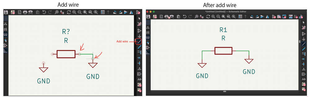
3-3) Global Label / No-connection flag
- Add Global Label to connect.
- Add a no-connection flag for the Pin that Not use.
3-4) Annotation
- Annotation assigns a number to every symbol
- If modifications to the schematic occur during the process, it may be necessary to re-annotate the schematic. In such a case, it is OK to execute the annotation again after clearing it once.
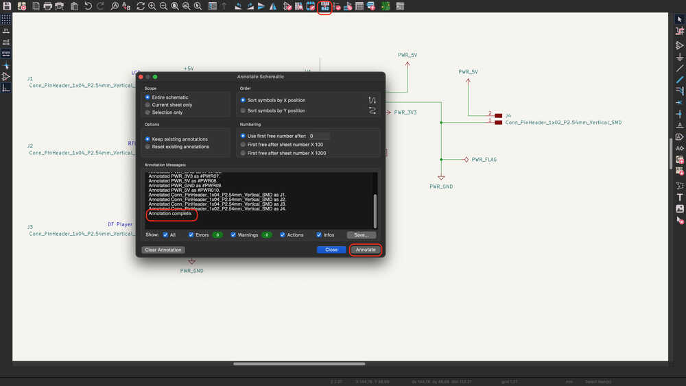
- If modifications to the schematic occur during the process, it may be necessary to re-annotate the schematic. In such a case, it is OK to execute the annotation again after clearing it once.
3-5) FootPrint
- Assign FootPrint, and select one.
- In case of resistor, I choose Footprint libraries and input the size. Then select one resister to use in the right section.
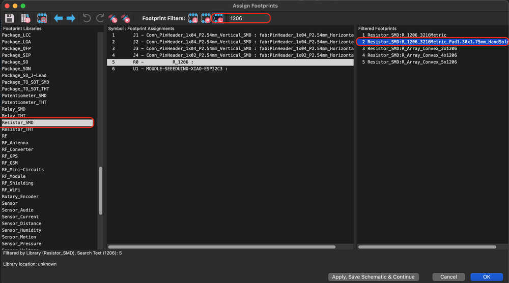
- In case of resistor, I choose Footprint libraries and input the size. Then select one resister to use in the right section.
3-6) ERC
ERC is an electrical rule checking tool, to check schematic. It aims to find electrical problems such as wrong connections, unconnected pins, missing power pins, etc. After a schematic is created or edited, it can be checked that the schematic is electrically correct by passing through the ERC.
- I do ERC, then, I see several Errors and Warnings in this schematic.
- At first, check wiring leaks and PWR FLAG addition leaks.
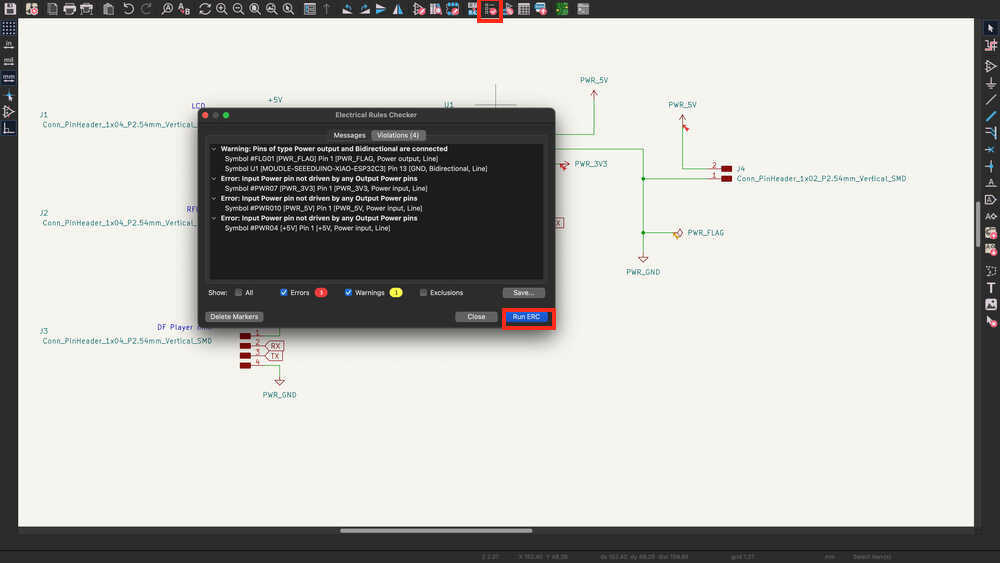
- At first, check wiring leaks and PWR FLAG addition leaks.
- I was stuck with ERC of PWR FLAG... I don't like this error. However, after several try, the error somehow disappeared!
4. PCB
Move to PCB. Before preceding with the board layout, I adjusted some Design Rules settings.
4-1) Design rule
- Set Grid (Default)
- Constraints (Default)
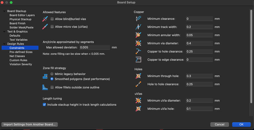
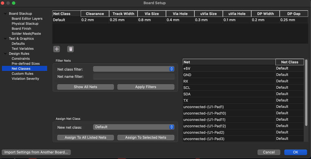
- Net Classes (Default)
- Pre-defined Size
(I added Power line width:0.8 mm, Signal line width: 0.4 mm)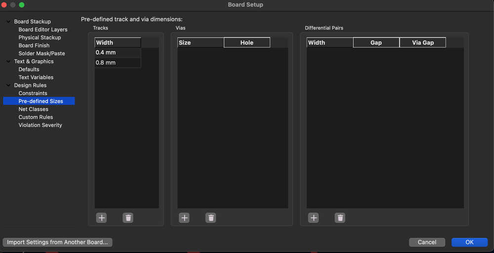
When I asked a question at Asian Review, the instructor Rico advised me the recommended size (Power line 0.8mm width, Signal line 0.4mm width). Thank you for advice!
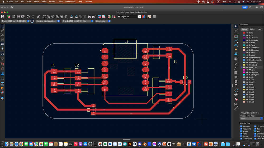
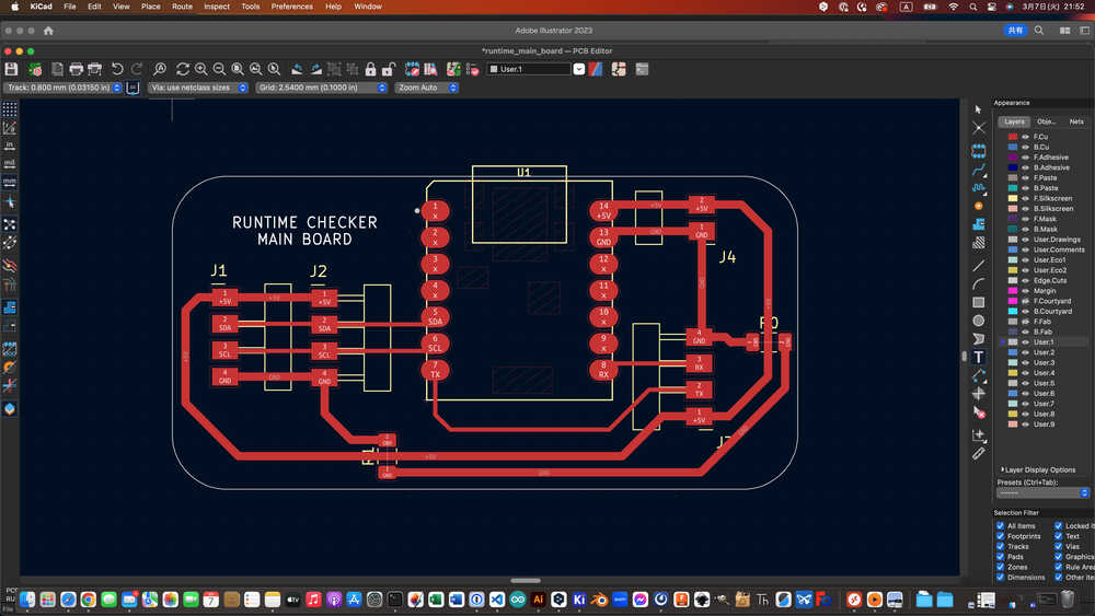
The design rule is done. start layout the board.
4-2) Layout the board
- Move to PCB from Schematic.
- Update PCB from Schematic, then click close.
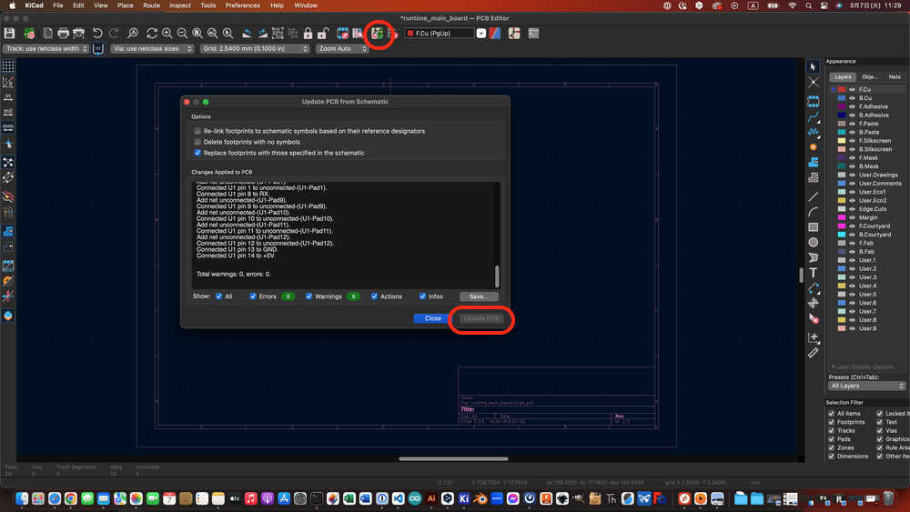
- The PCB parts are update.
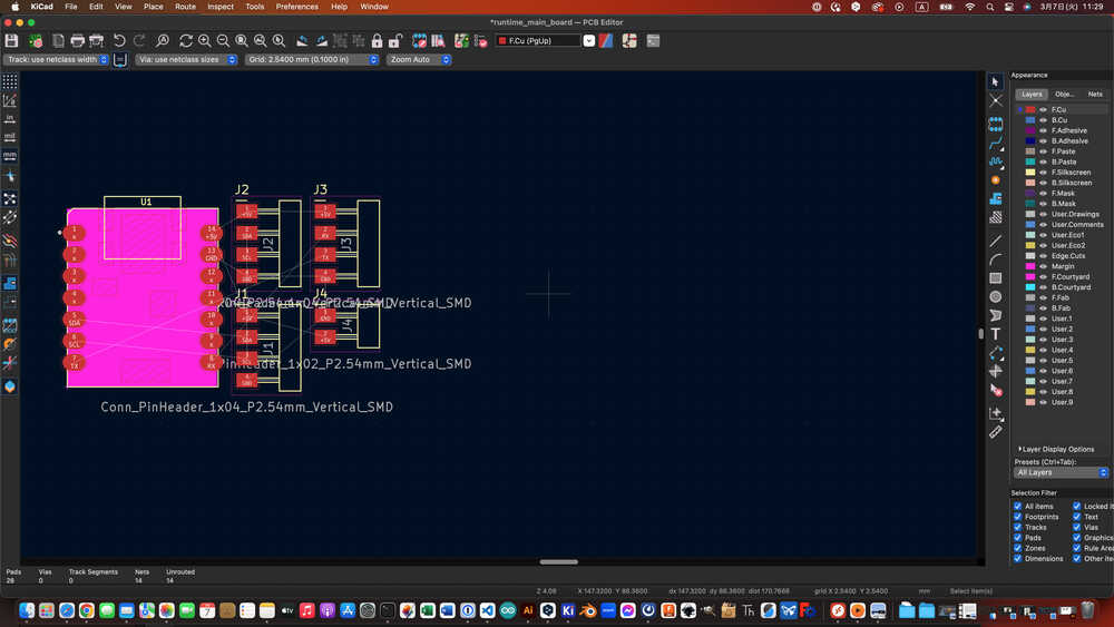
- Move the each PCB parts and add wire.
- I can't complete the wire, so Move to Schematic, add the Resistor 0Ω.
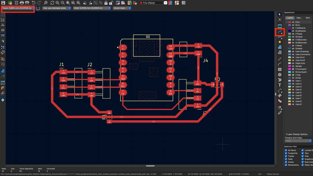
4-3) Edgecuts
-
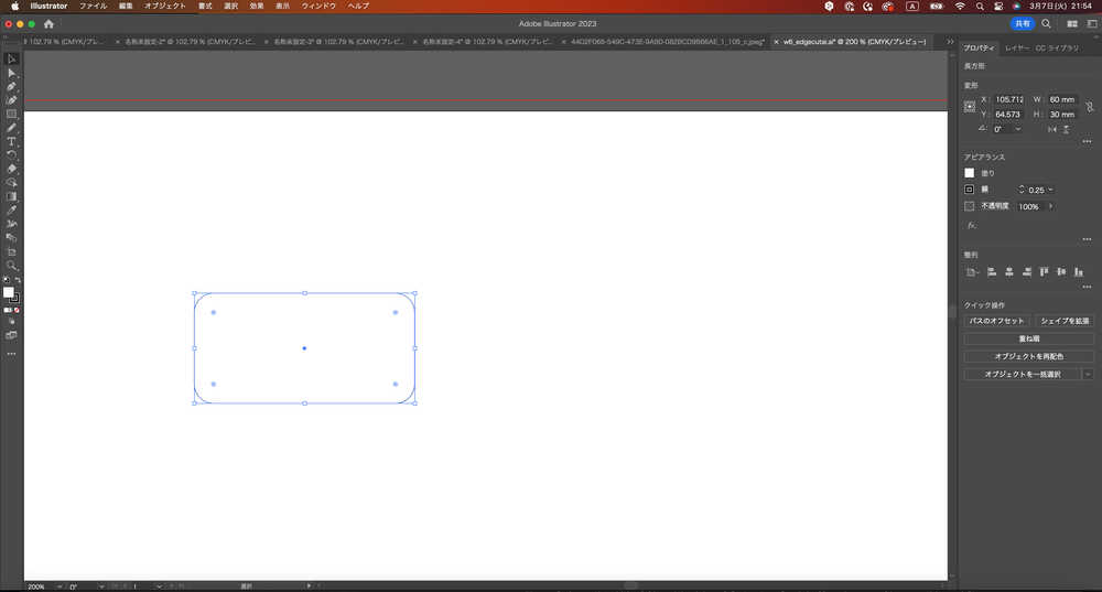
Move to illustrator, and I made edgecuts with illustrator. size: 30 x 60 mm with R
-
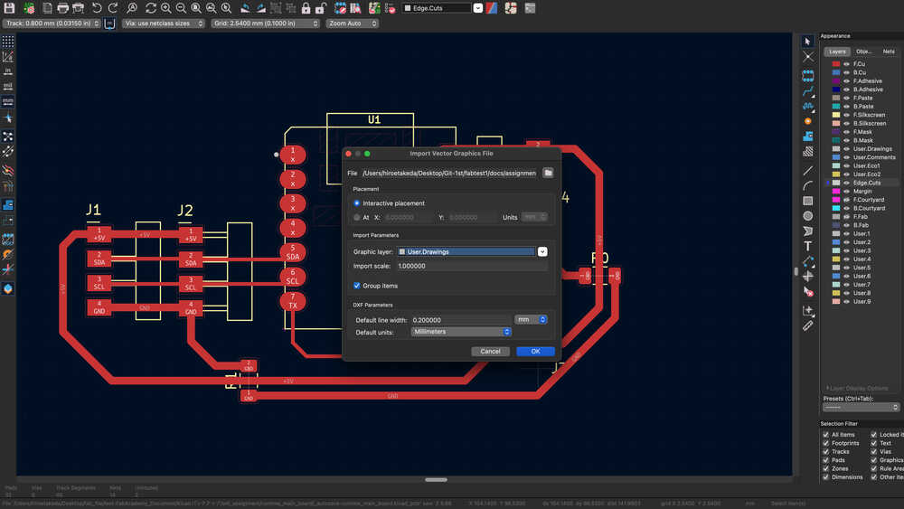
Move to PCB, Click the Edge cuts on the right menu, Import the Edge cuts to PCB new. (NOTE: This action make trouble later with DRC, as I was chosen user drawing. Please choose "Edge cuts" correctly. )
- Prototype1 is done.
4-4) DRC
The DRC is Design Rules Check (physical rules check) in board layout. These include line widths, clearances (distances between traces and pads), etc.
-
When I did DRC for this board, I stuck a lot of warning.
-
The Most warning were "Track has unconnected end"
-> In Kicad when wire are moved, often leaves so short wires that they are overlooked. In my case, I didn't realize it and got a lot of these errors. The error was resolved by delete them.
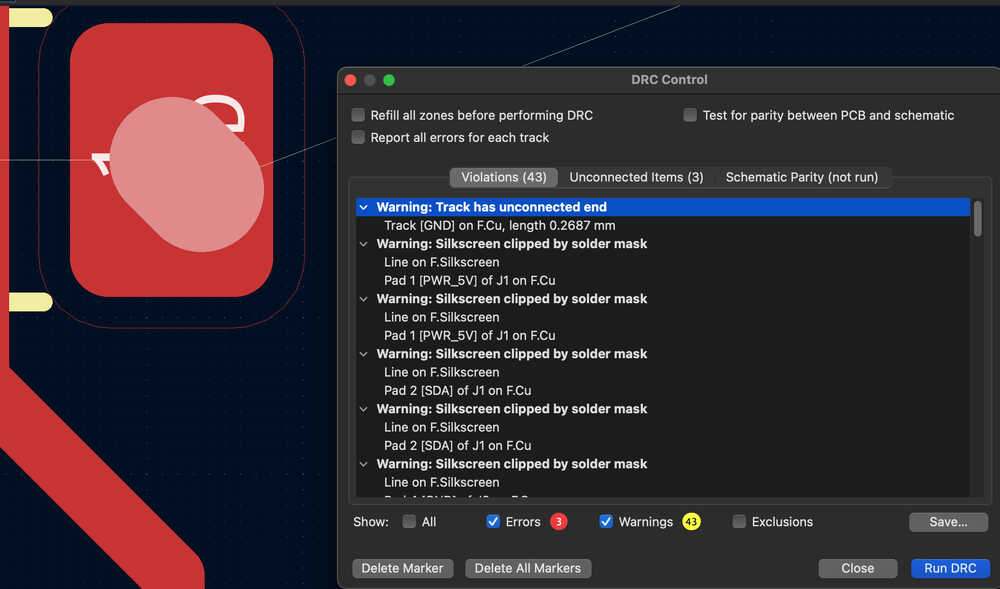
- The warning "Silkscreen clipped by solder mask"
-> Check the parts are cut or covered with solder mask
refer to Youtube - The warning "No Edge cut"
-> Check Edge cut is made. - The warning for "Resister 0ohm (the resister to use instead of jumper wire) is unconnected "
-> I think, It is OK to ignore for the milling and soldering in our lab.