Work log - Week 6 - March 2, 2022
3/2 - Wednesday
Class Links
From Electronics Lecture
SAMD11 Base board pcb design: https://circuitmaker.com/Projects/Details/LtFlash/SAMD11-Base-Board
https://fabacademy.org/2022/labs/kannai/Instruction/tips/matterport/
https://my.matterport.com/show/?m=St6GemLevW2
https://fabacademy.org/2022/labs/waag/students/bas-pijls/blog/week5/
https://web.media.mit.edu/~achoo/polar3D/
Meshroom Polarized light scanning
https://fabacademy.org/2022/labs/kamplintfort/students/jan-bewersdorff/assignments/assignment_5.html
http://fab.cba.mit.edu/classes/863.15/section.CBA/people/Liu/index.html
Went to class. Spent today catching up on documentation, checking out how some of the 3d prints that we started last night turned out (they came out well.)
3/3 - Thursday
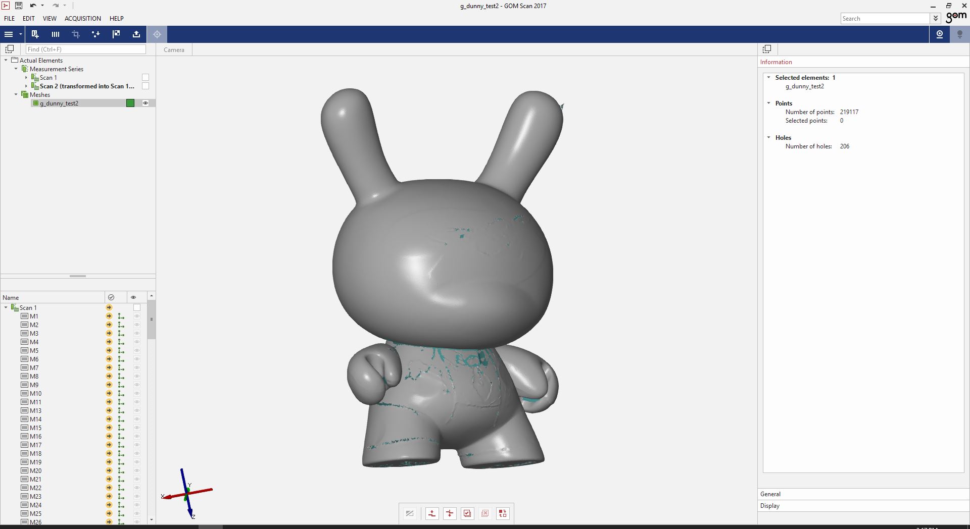
Spent a large amount of time today working with the GOM scanner. I had used it once, briefly, over 2 years ago. There was a large learning curve, and may mistakes and errors were made. I feel like I’ve gotten 70% to making a good scan, but I also managed not to actually save an STL file on my flashdrive!? I’m still missing some things like how to transform and combine multiple scans into one object. I also need to work on the most efficient way to clean up scans and get them into formats other than stls.
3/4 - Friday
Met with Adam and Cori in the soldering lab at CPCC. We helped Cori finish up her programming board. I soldered up one of the new printed AH programming board. Bothered Adam with lots of questions as well opinions.
3/5 - Saturday
Spent a large chunk of the day working on documentation. Adding and making changes to previous weeks.
Also continued work on a new SAMD11C board I’m designing. There is a lot of “I’ll do it this way.” only to find out I should have done it some other way. I don’t know enough to know what I’m doing. It’s slow, but I’m becoming slightly better at KiCad.
I’m trying to create a USB PCB edge connector footprint in KiCad. I couldn’t find this footprint anywhere, even though everyone seems to be using it.
Got help from: https://forum.kicad.info/t/tutorial-how-to-make-a-footprint-in-kicad-5-1-x/11092
3/6 - Sunday
USB PCB Edge Connector for Kicad
Worked a lot on making a USB PCB footprint for KiCad. I looked and I couldn’t find one. It wasn’t until today I realized they’re often called “USB PCB edge connector”, but even then, I couldn’t seem to find one for the Kicad library, so I had to go and make my own. This alone probably took an hour of time, learning how to make a library (it’s easy, once you know you have to do it and how to do it. You can’t just add to existing libraries.). Then learning how to add the connector to the schematic, adding and drawing the footprint, and then connecting the two so that it appears on the PCB view.
Here it is: Garrett’s USB PCB Edge Connector footprint for Kicad
New SAMD11C pcb with ADXL343 Accelerometer
I also worked just about all day on creating a better design for a SAMDC11C and ADXL343 pcb. That said, it’s still quite the learning experience, and a work in progress.
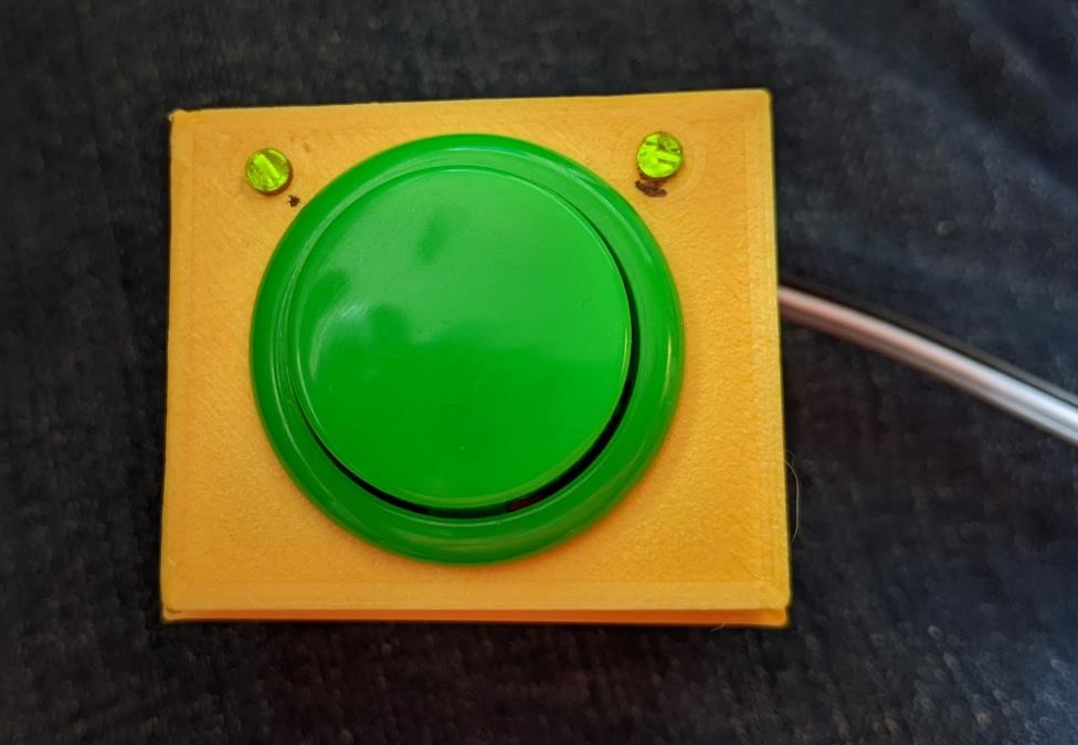
Blinky Button Case
I also made a case for this week’s assignment of a re-drawn blink board. However, with the button I’m using, I need a decent sized case, and I also wanted to be able to see the LED’s, and it’d defeat the point if you couldn’t see those LEDs anyways.
So I made a case and I added light pipes to it. This is 3.5mm plastic “fiber optic” rod that I cut and bent into shape so that it would align just over the two LED’s on my board.
I used just bigger wire snips to cut the plastic rod, and just a bit of heat (I used a lighter) will soften the rod and allow you to form it to shape. Just don’t over due it with the heat.
Then I added a small 3d printed part to help align the two rods right over the led’s, and after I got it situated, I added a bit of hot glue to the top of the case to keep it all in place.
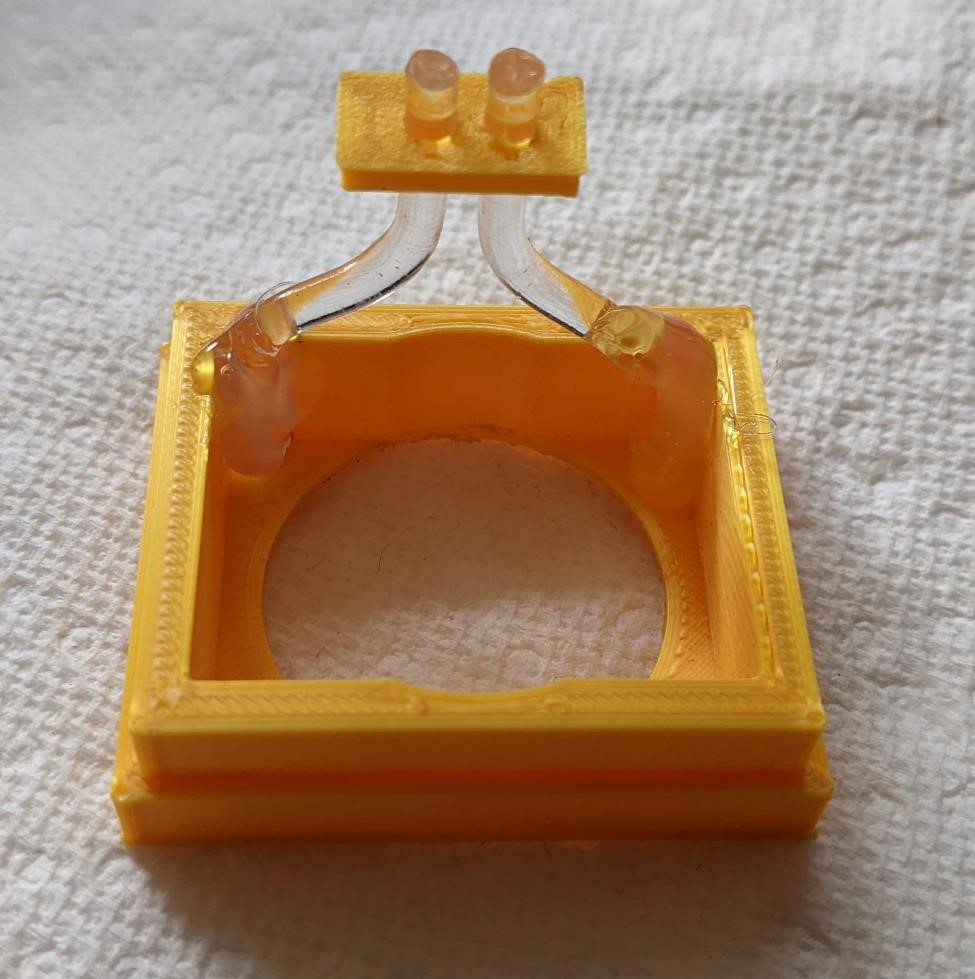
and the final case:
3/7 - Monday
Still working on more advanced PCB’s -SAMD11C pcb with ADXL343 Accelerometer and Neopixel (WS2812B)
I also worked just about all day on creating a better design for a SAMDC11C and ADXL343 pcb. That said, it’s still quite the learning experience, and a work in progress. (This is deja vu all over again.) I’ve removed some of the pins, and included a neopixel RGB led.
I finally came up with a “simpler” design that I think can work. However, now the problem becomes how to make it.
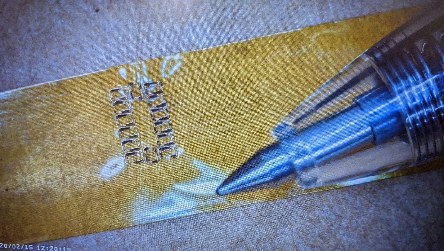
Preparing solder paste stencils for laser cutting
I’ll need a tiny 0.1mm endmill to cut out the board, and then a hot plate and paste to solder the ADXL343 onto the board. And in order to use the solder paste, I’m going to have to create a stencil.
I took the SVG into Inkscape, and thankfully, because when you output the Plot from Kicad, it creates the pads and traces seperately, it’s quite easy to just select all the traces and delete them (I know there’s a way in KiCad to create a stencil, but I discovered this by accident as I add names and voltages in Inkscape, and this was a quick enough way, I didn’t worry about the Kicad method. And I had to import it into Inkscape anyways). Once I have just the pads, I can select them all and change the line width to 0.1pt and the stroke outline to Red. This will make the part ready for laser cutting in some Kapton tape to create a stencil.
3/8 - Monday
- Worked on getting the GOM Scanner documented.
- Also managed to get a good scan of the test piece and a STL. The STL still needs to be cleaned up.
- Tested the laser cutter and Kapton tape. I think I’ve got a good methodology for producing tiny stencils. They’re not super clean, but hopefully they’ll work. It’s a starting point.
- Spent a lot of time with Cori working on Kicad and milling out some boards. Took about as long as expected. Blind leading the blind.
- Worked on the group project trying to use an oscilloscope. Managed to turn oscilloscope on.
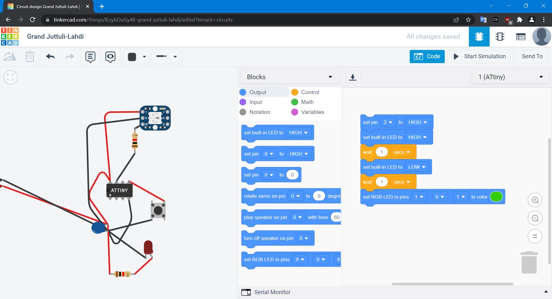
- Started working with Tinkercad and it’s electronics simulations. Modelled a simple blinky light.
- Updated a lot of documentation.
- Went to bed, very tired.
Weekly Resources:
This was timely: https://learn.adafruit.com/working-with-i2c-devices