7. Electronics design
Week 6 - 3/2/22
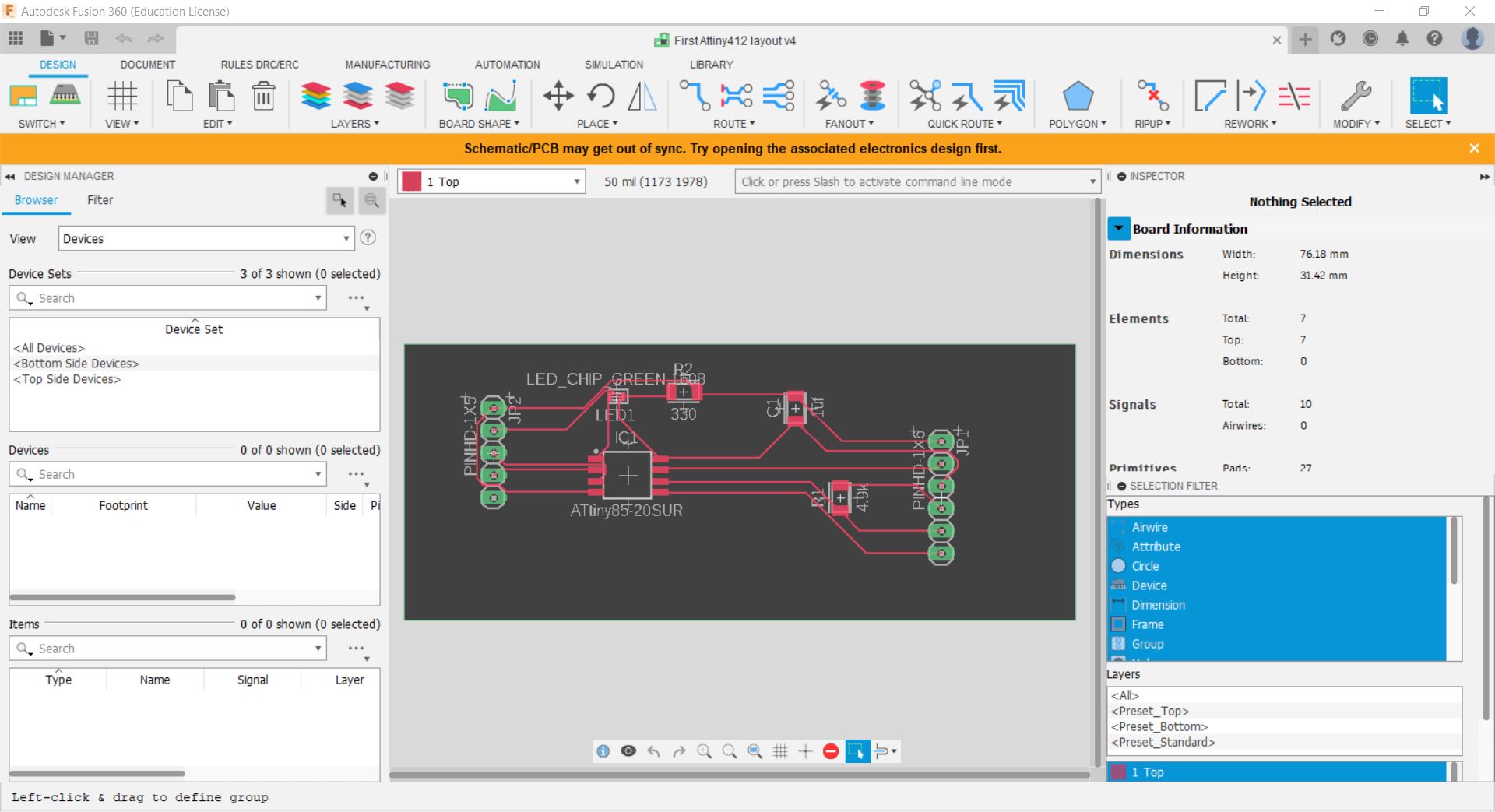
This week we focused on designing our own pcb’s (well, really MCB’s)
This page is broken up into two main sections.
The first is a quick and dirty build of an Attiny412 based board.
The second is a more in-depth look, and more tutorial based build of an SAMD11C board.
A note on software.
Fusion 360
Eagle used to be it’s own electronics design software. Now it has been incorporated with Fusion 360. I tried using Fusion 360’s software. It didn’t go very well.
I know I’m just learning, but it was just things like choosing components to move was incredibly difficult unless you clicked on exactly the right pixel.
I couldn’t find the parts I needed in the reference library (the Attiny1412). Now I know a little bit more and I could probably input my own footprint and schematic, but at the time, this is something that a) I didn’t know how to do. b) I didn’t want to do. c) I shouldn’t have had to do.
And things didn’t improve much from there. To it’s credit though, some of the skills I learned from this experience applied directly to the next software I used:
KiCad v5
While KiCad had it’s own quirks, flaws and irritations; I found I could make a schematic fairly quickly. The parts were in the library, and while I actually enjoyed Fusions 360 “tutorial library” that also includes footprints with the symbology, I also realized the nicety of just creating a schematic free from physical constraints (at first, then came the routing.)
Note that I’m using a slightly older version of Kicad, but the new version is v6, and it has some differences between the instructions below. However, for the most part, the basics are the same.
I would also suggest getting to know the kicad hot keys very quickly. You’ll be using them a fair amount.
Design Notes:
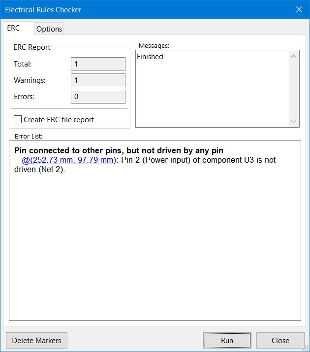
You may have an “error” when you check your board with the “Perform Electrical Rules Check” due to Kicad apparently not understanding where the power is coming/going. This is where I just found someone who said that adding “PWR_FLAG” is the way to “fix” this issue. From: https://forum.kicad.info/t/errtype-3-pin-connected-to-some-others-pins-but-no-pin-to-drive-it/10946
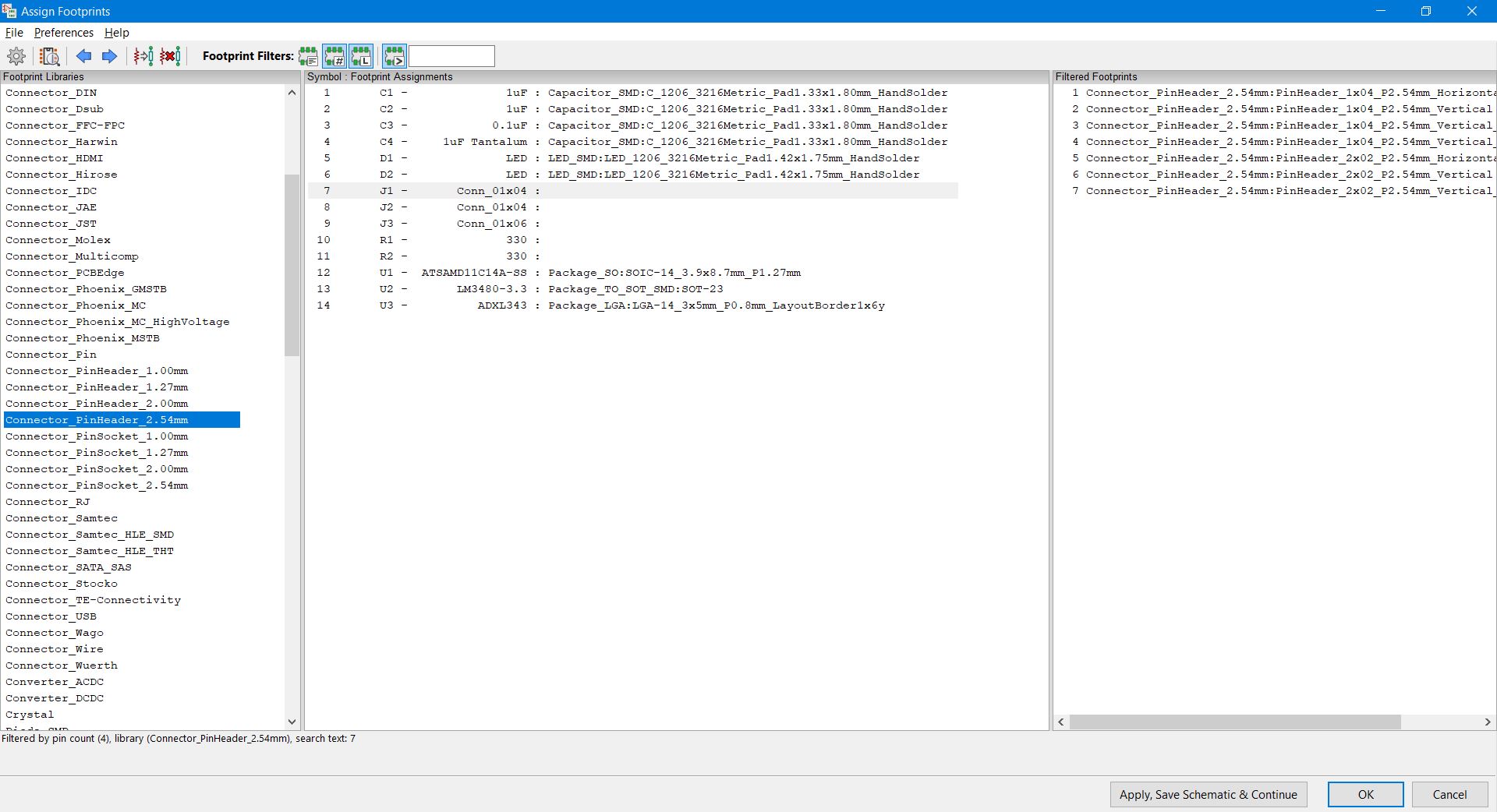
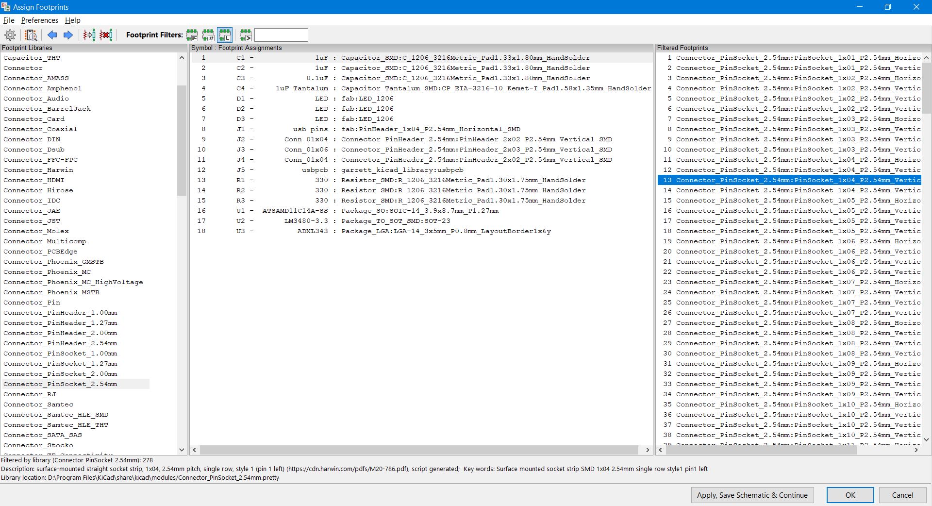
You need to “assign PCB footprints to schematic symbols.” In order to do this effectively, you need to know what types of parts (their “packaging” not just their values) so that you can design a board to be quickly milled and soldered. At CPCC, we’re using a lot of “1206” smd components.
When you’ve created a schematic, click on the “netlist” button. This creates connections between components for when you start designing the PCB.
It’s easier to change the trace thickness sooner rather than later. So when you start drawing the PCB, you want to do this ASAP. I changed mine to 0.400mm (400 microns)
You may also have to change the pin’s that you connect the microcontroller too in order to get better/easier routing. I only know how to do this in the schematic view. Be prepared to do this.
Since we’re milling these boards, make sure to have at least 1 tool diameter (in our case, 1/64th tool, 0.0156”/0.40mm) btween all the traces and component pads. In actuality you probably want much more than this, but this is the minimum.
Also possibly helpful for KiCad: https://blog.mbedded.ninja/electronics/general/kicad/kicad-tips-and-tricks/
Design Questions
Knowing very little, I had a bunch of questions:
Did I need a crystal for the Attiny412/SAMD11 : Apprently No.
Do I need pull up resistors for the I2C communications for the 412/samd11 : I don’t think so?
UPDATE: I Think I may need 5k to 10k pullup resistors for SDA and SCL? ( See: https://www.instructables.com/I2C_Bus_for_ATtiny_and_ATmega/ and https://www.gadgetronicx.com/attiny85-i2c-protocol-tutorial/) The good news is that this is an easy fix.
https://blog.mbedded.ninja/pcb-design/pcb-design-checklist/
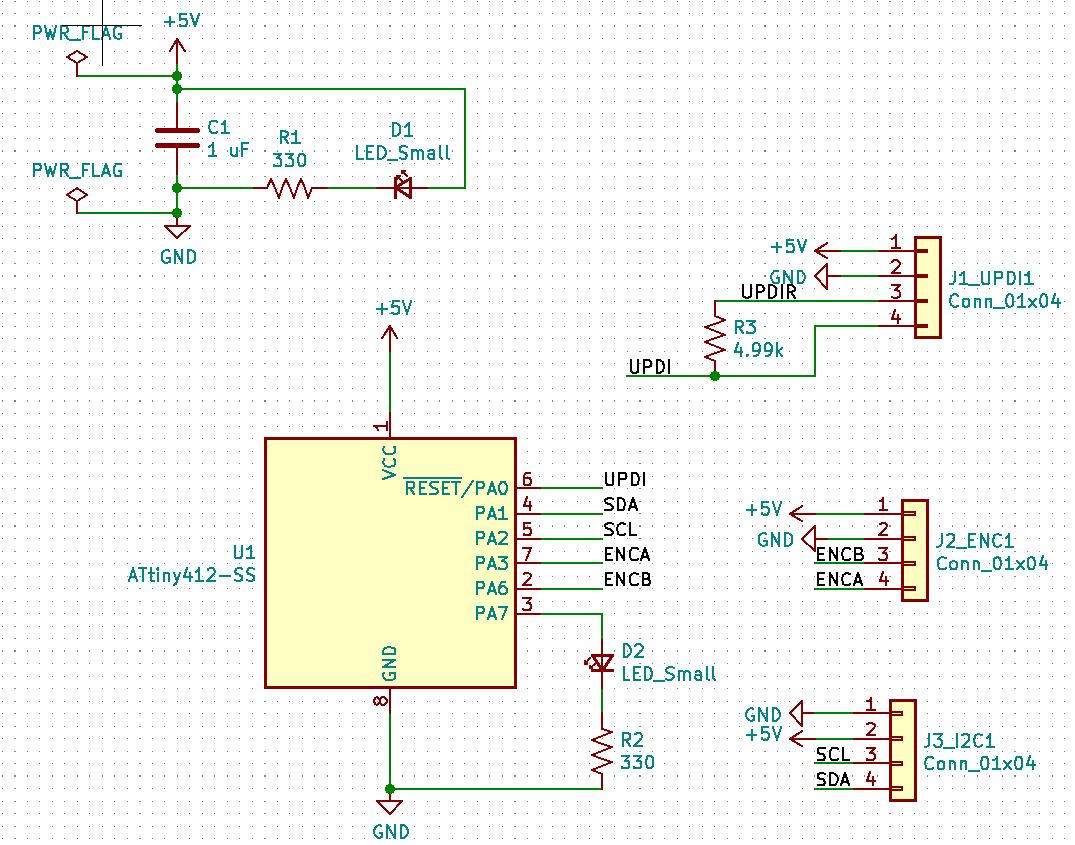
Attiny 412 Board
Design and Schematic
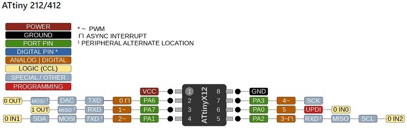
This board is based around the Attiny 412 chip. Below is the image of the pinouts, and what each pin does, or is capable of.
I’m basing my board around a “blinky” attiny412 board by Adam Harris, as well as a number of other boards I’ve seen on Neil’s website, as well as other FabLab sites (see References below.)
I’ve essentially copy and pasted schematics, because I have no idea what I’m doing.
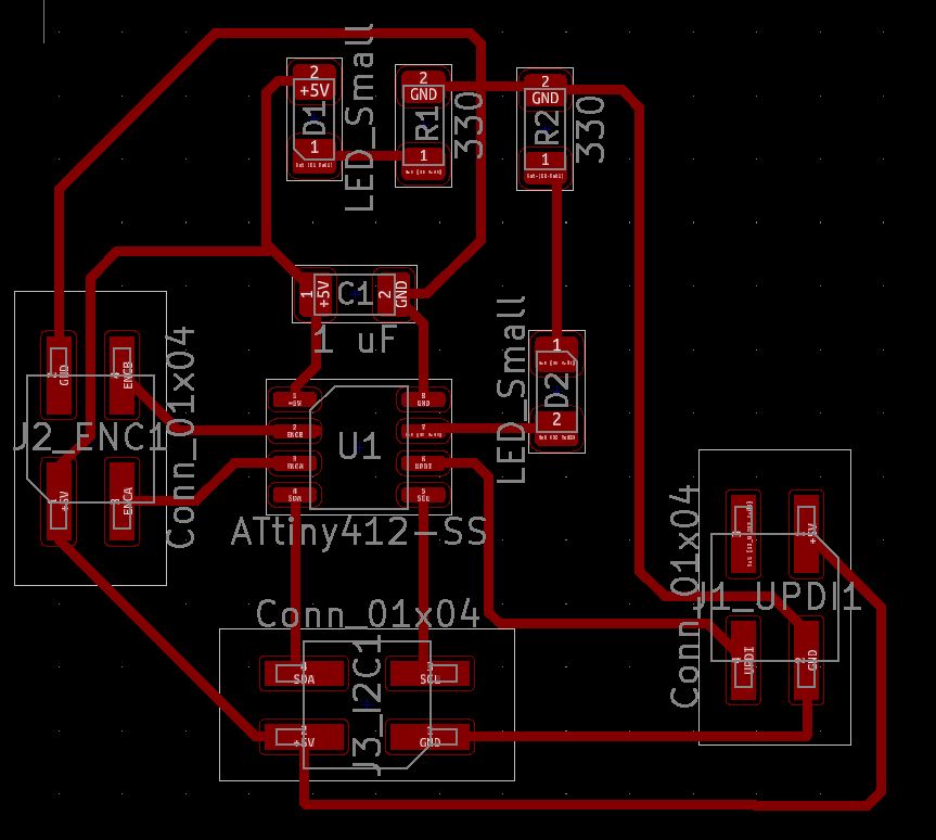
And after a bit of a learning curve, I finally got to this point: A PCB.
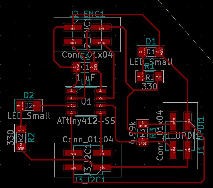
Following the two videos posted on Adam Harris’ site: https://sheekgeek.org/2022/adamsheekgeek/how-to-export-to-a-cnc-from-kicad-and-fab-mods
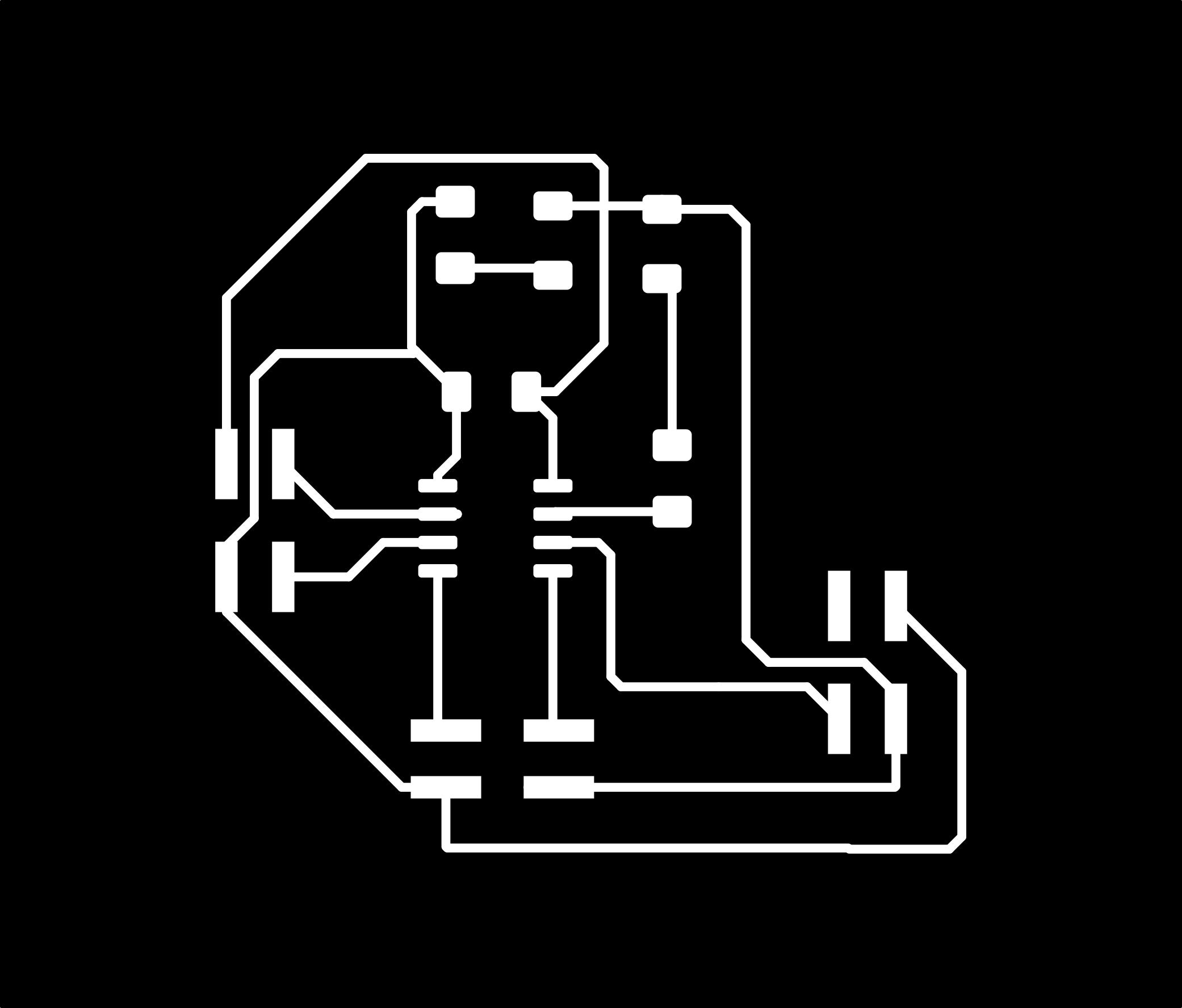
Final Design Files
I managed to turn it into an PNG file ready for mods and milling.
v2 of the pcb design:
The traces file for Mods:
and the outline file:

And a render of the board, that’s missing the IC.
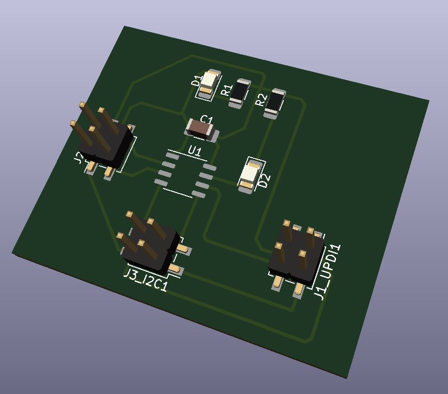
You can try and add the IC, though it should be in the library already, but I had some funky things going on with the permissions, and I didn’t bother tracking it down. It’s a render. Just imagine the IC is there.
More info on how to add 3d model components: https://www.youtube.com/watch?v=NRsmNiNQHks
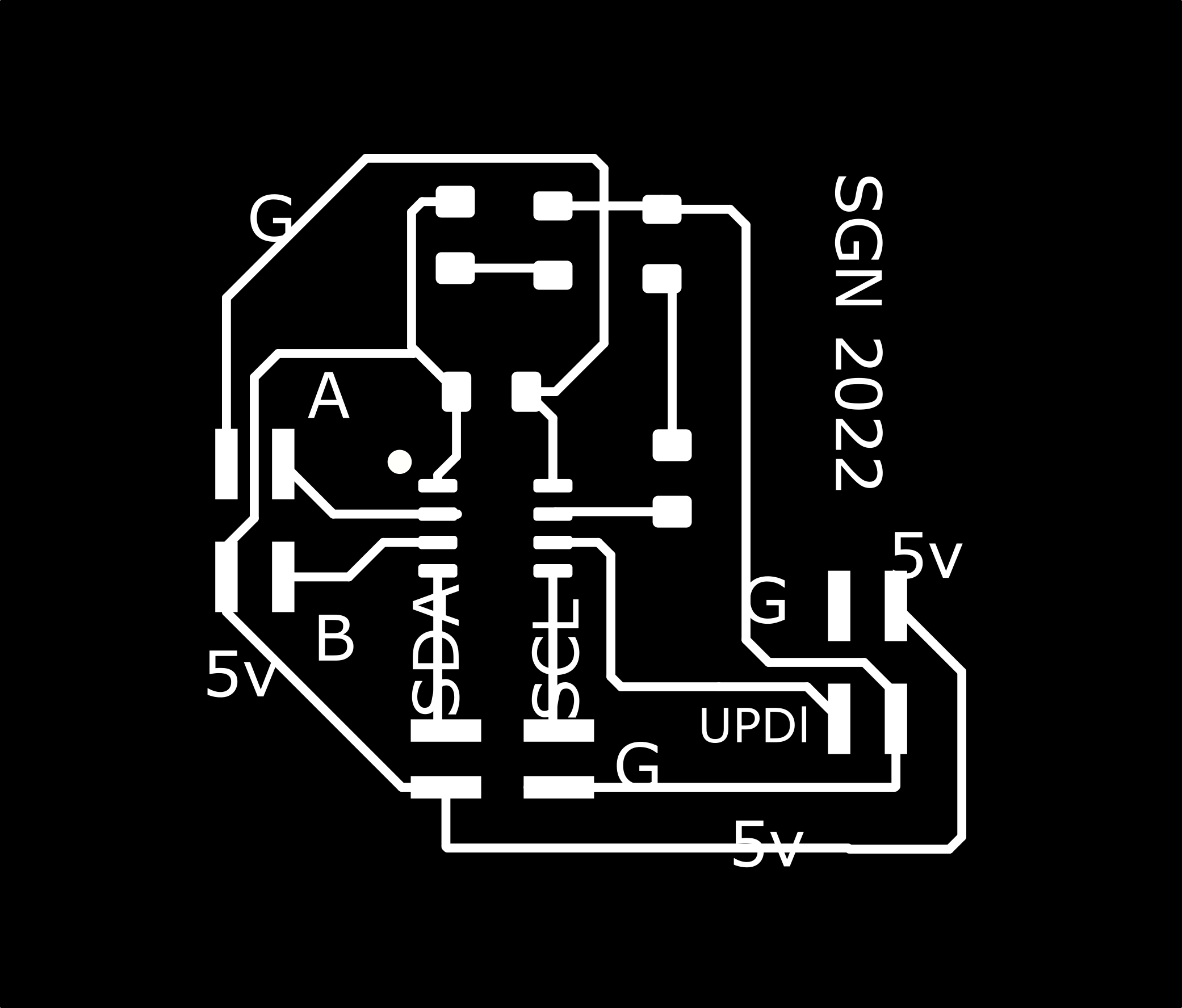
Adding notations
I took the SVG file that was created from the “plot” in Kicad, and opened it in Inkscape.
Here I simply used the letter tool to add notation to the board, adding “G”, “5V”, “SDA”, “SCL”, etc. on the board to help with remembering which pin is connected to what. I used a size 8 font, and it seemed to mill very well with the 1/64th bit.
The Components
| Designator | Component |
|---|---|
| U1 | ATTINY412 |
| J1, J2, J3 | 2x2 SMD pin header |
| C1 | 1uF 1206 |
| D1, D2 | Red or Green LED 1206 |
| R1, R2 | 330 ohm 1206 |
Milling and Stuffing
I’ll be following the procedures from Week 4/5, where we milled the board and then, stuffed and soldered it.
The board was milled and stuffed. I did a poor job of documenting this, because, well, I’ve done it before. See above.
Programming
Again, see Week 4/5
For a quick test, I used Neil’s blink code.
I refined Adam Harris’ with notes on using it with various boards (different pin outs for LEDs)
This was programmed with the Arduino IDE, using our programming board.
//Adam Harris
//https://sheekgeek.org/2022/adamsheekgeek/samd11c-multi-use-board

int led = 4;
//2 for samd11 programming board
//3 for Neil Blink board
//4 for Garrett i2c board

// the setup routine runs once when you press reset:
void setup() {
  // initialize the digital pin as an output.
  pinMode(led, OUTPUT);
}

void loop() {
  digitalWrite(led, HIGH);   // turn the LED on (HIGH is the voltage level)
  delay(800);               // wait for a second
  digitalWrite(led, LOW);    // turn the LED off by making the voltage LOW
  delay(300);               // wait for a second
}
Blink.
It blinks.
And it has a button. (because I hate those crappy little SMD buttons, and I wanted to make this a more extinsible board in a case, I added pins for an external button.)
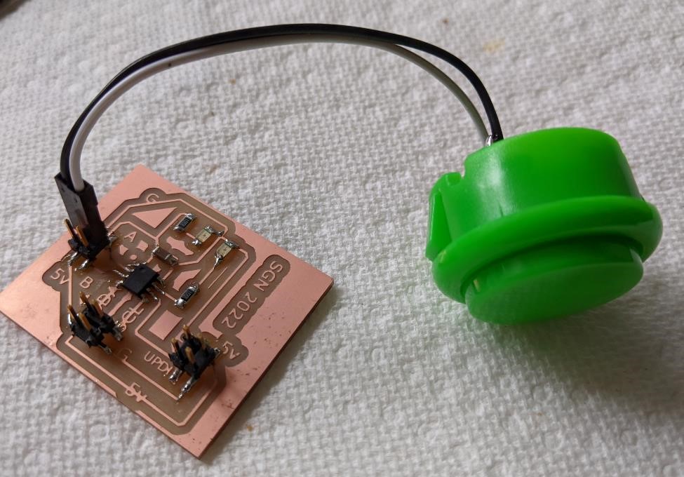
And it has a case.
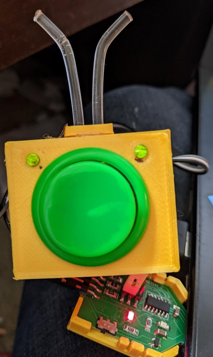
OpenSCAD files for this case can be found here
I’ve also programmed it to light up the LED when the button is pushed. (silly to use a microcontroller to light up with a button push. But hey, got to start somewhere.)
//modified from code: https://arduinogetstarted.com/tutorials/arduino-button
//sgn march 2022

const int BUTTON_PIN = 0;
const int LED = 4;

int currentState = LOW;    // the current reading from the input pin

void setup() {
    pinMode(BUTTON_PIN, INPUT_PULLUP);
    pinMode(LED, OUTPUT);

}

void loop() {
    currentState = digitalRead(BUTTON_PIN);

    if(currentState == LOW) {
        digitalWrite(LED,HIGH);
    }
    else
    {
        digitalWrite(LED,LOW);
    }
}
Getting the Attiny412 Echo code working.
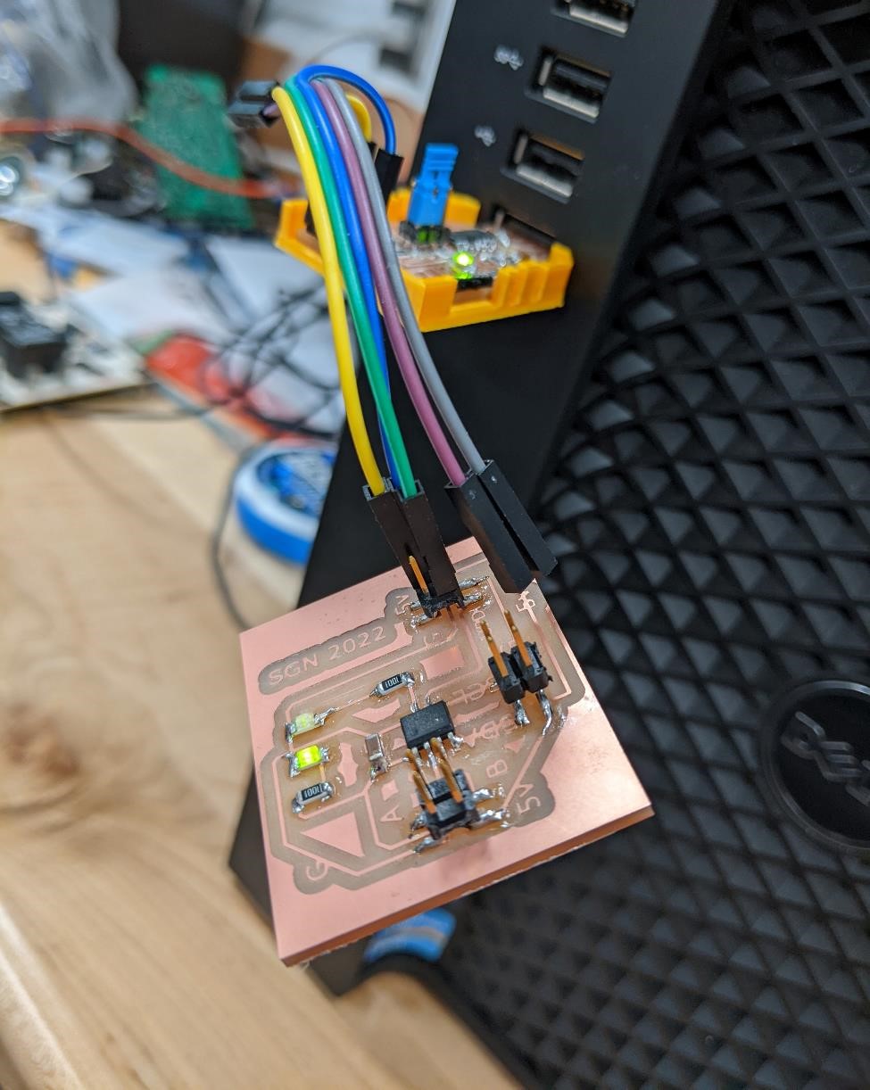
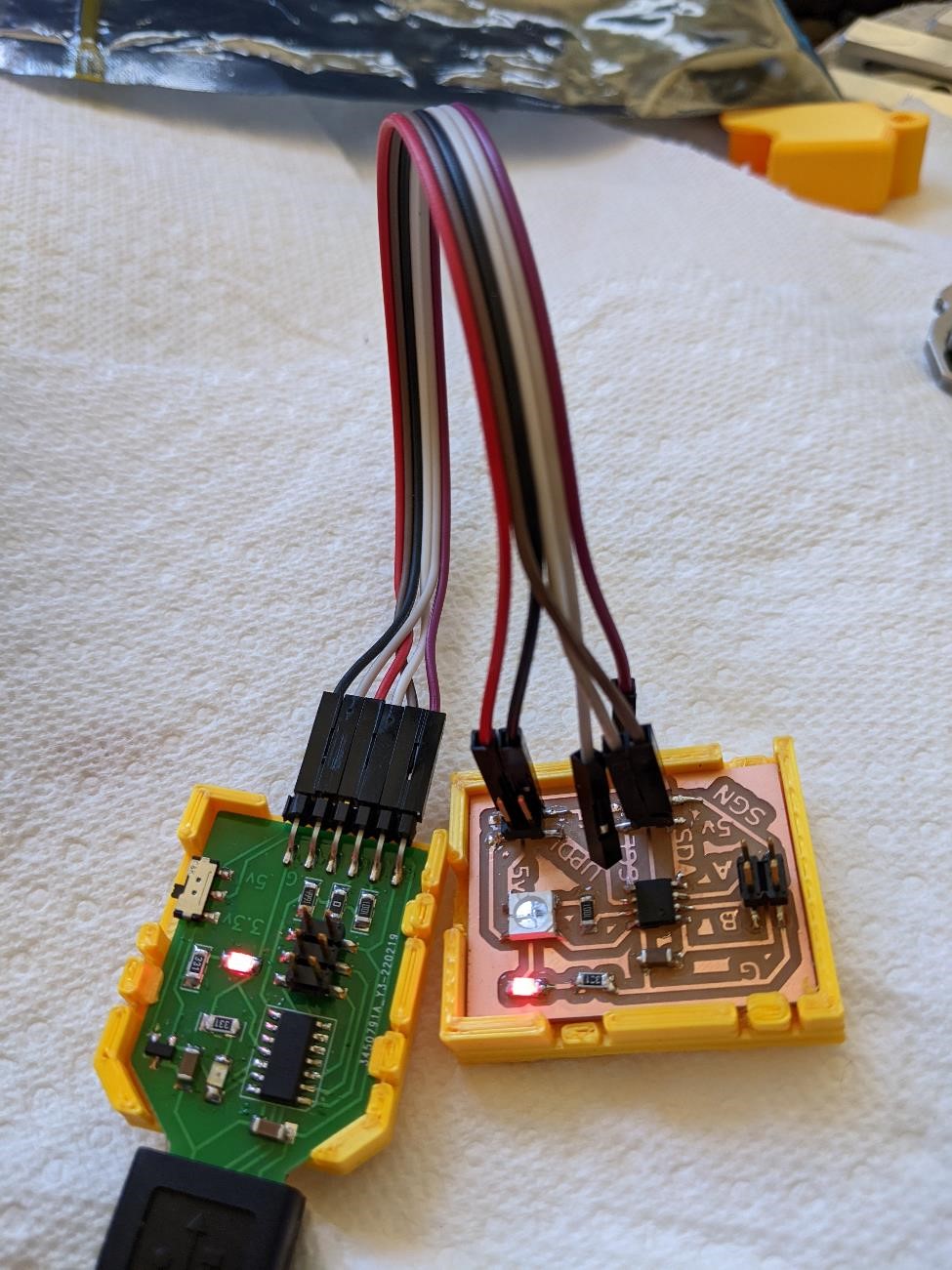
After programming the board with the Tiny412.echo code from Neil, found here: http://academy.cba.mit.edu/classes/embedded_programming/t412/hello.t412.echo.ino and using Adam’s programming board to upload the code via UPDI, I tested it. For more on how to program these boards, see Week 5.
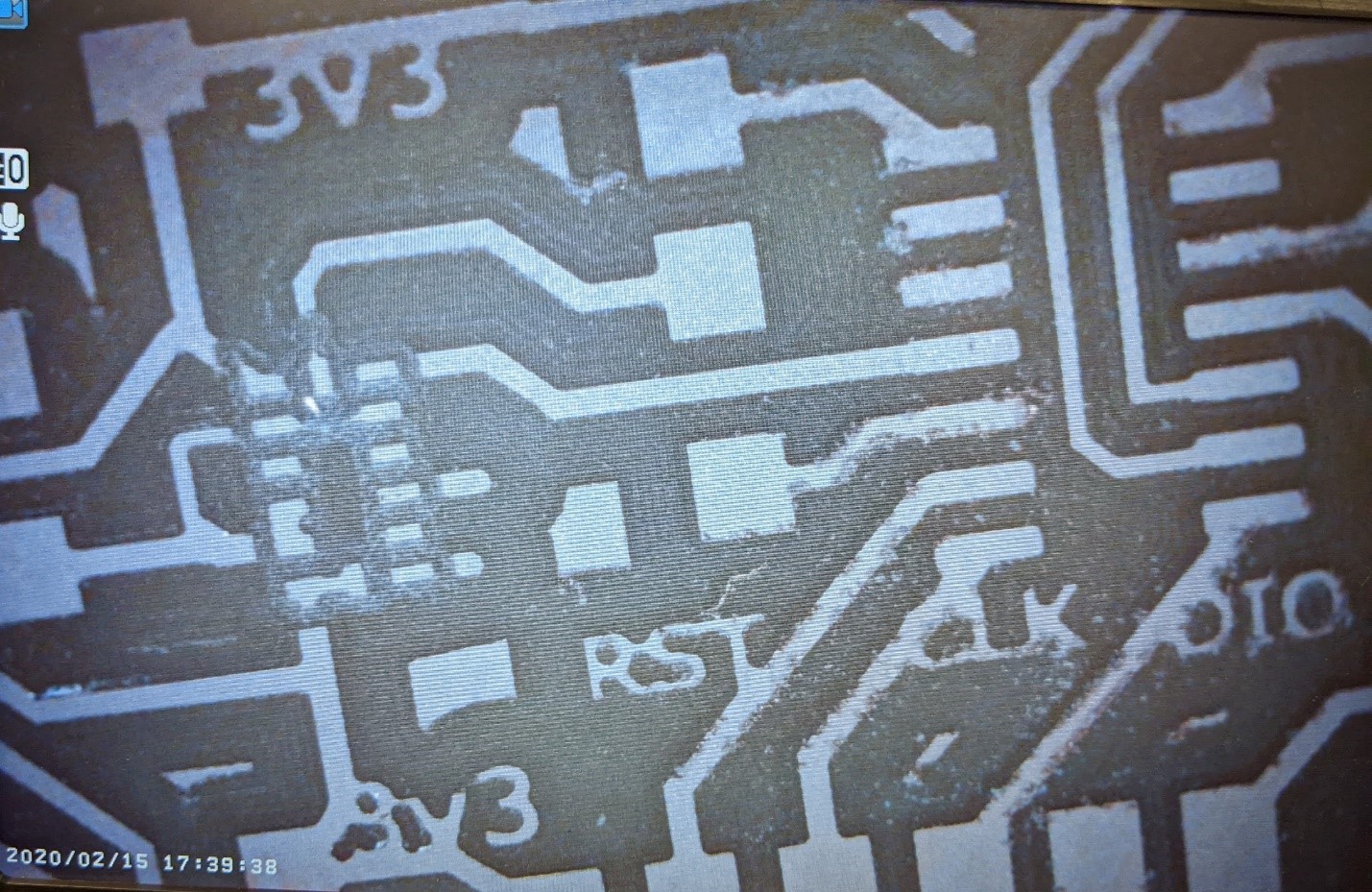
I hooked the board up to Adam’s programmer, configured for reading UART’s (or so I thought) and programming UPDI.
I hooked up the board following this image of Adam’s board pinouts:
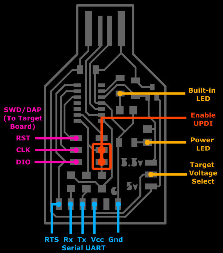
For the Attiny412, the RX pin is the physical pin 5, and the TX pin is the physical pin 4.
Remember, you must connect RX to TX (and vice versa) when connecting serial between two pcb’s.
I hooked the TX pin on the programmer to the RX pin of the Attiny412 board, and the RX of the programmer to the TX pin of the tiny412, as well as ground to ground, and 5v to 5v.
And then I went to the Serial Monitor of the Arduino IDE to test this program. But I was disappointed. At first I did not receive any data. Finally after playing around with wiring, settings, baud rates, etc. I discovered that there was an issue of a cold solder joint on my header pins on my attiny412 board. I fixed this, but still had issues.
After coming back to this weeks later, I finally dug into the problem.
I was able to get some gibberish from my board, but it was inconsistent and odd.
I came up with a very simple example, very loosely borrowed from Neil’s (and every other basic serial test code), for testing purposes. It just repeats “hello” every 1 second, and gives me something to know if the data is being received or not.
void setup() {
   delay(300);
   Serial.swap(1);
   Serial.begin(57600);
   }

void loop() {
   if (Serial.available() > 0) {

      Serial.println("hello there.\");
      delay(1000);
      }
   }
This time, I was able to get consistent gibberish.
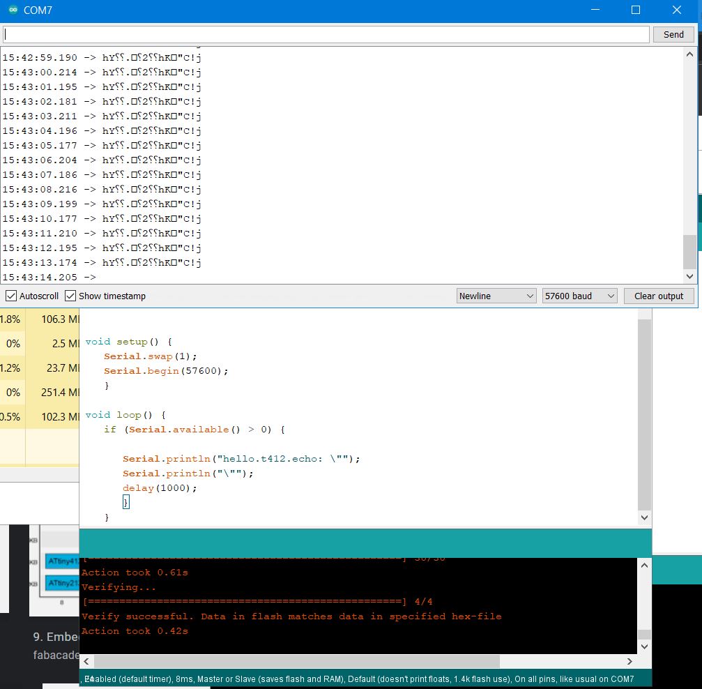
I played around with baud rates, and their effect was zero. It didn’t matter what the baud rate was. This threw me for a loop for a few minutes, but then I realized that this indicates that it’s likely not a hardware issue, and if anything it was probably related to the “programmer as a serial interface.”
I checked out the basic code that Adam had written for this serial to serial interface for programming UPDI and discovered the issue.
Adam’s Code:
void setup() {

   SerialUSB.begin(0);
   Serial1.begin(57600, SERIAL_8E2); //Adjust baud rate and use SERIAL_8N1 for regular serial port usage
}

void loop() {
   if (SerialUSB.available()) {
      Serial1.write((char) SerialUSB.read()); //Send stuff from Serial port to USB
   }
   if (Serial1.available()) {
      SerialUSB.write((char) Serial1.read()); //Send stuff from USB to serial port
   }
} //end loop
The problem is in the third line of the above code, and even states the issue. I should have paid more attention to this the entire time.
In that simple little serial to serialUSB UPDI programmer code, it has:
Serial1.begin(57600, SERIAL_8E2);
For some reason it’s set too: 8 bits, Even parity and 2 stop bits. (I later asked Adam and he told me that UPDI requires 8 bits, Even parity and 2 stop bits to work.)
I changed it to no parity and 1 stop bit (pretty normal serial setup, and like I said, the code actually specifies this in the comments.
Serial1.begin(57600, SERIAL_8N1);
and it works like a champ (at least it’s not spitting out gibberish.)
I tried to program with UPDI having this setup, but it does not work. It does require the serial to be set to “SERIAL_8E2” to work as the UPDI programmer.
However, if you need to simply have a serial interface, you’ll need to re-program this same code with the change to “SERIAL_8N1”.
And that was a lot of time wasted just to get a board to spit out data. But I needed this serial output to work for my other boards, so it was worth figuring out and fixing this problem.
And for more information about Attiny412 and the serial interface, check out: https://github.com/SpenceKonde/megaTinyCore/blob/master/megaavr/extras/Ref_Serial.md
What the hell is going on with Pinout/PA/and physical pins?
I don’t know. But be very careful. Your physical pin number may not be the same as what you define as the “pinout” in an arduino sketch.
I found the answer to this, and a lot of great information here: https://github.com/SpenceKonde/megaTinyCore (search for “Pin Numbers”)
Simulating a blinking ATtiny.
David Taylor at Charlotte Latin had told be about Tinkercad, and Neil mentioned it during the last class. So I gave it a try to simulate a basic circuit similiar to the one I designed above.
There are a number of differences, the most extreme being this simulates an attiny45/85 and I used an Attiny412 on my board. While for such a simple project, it doesn’t matter, but the pins for Vcc and Gnd are different between the two IC’s.
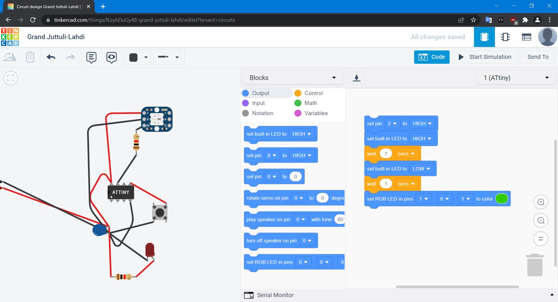
And I’ve never used the “scratch” style programming interface, and frankly I wasn’t willing to spend too much time on simulating this circuit (Though I do plan on spending more time with the electronics simulators in the future, I had run out of time this week.) and learning yet another style of programming interface. So once I got the thing to blink, I was done.
But hey, it blinks.
Creating a new SAMD11 Board
Making a simple blinky board wasn’t too terribly difficult. I essentially relied on other board designs out there, including Adam Harris’, Neils’, Quinten’s, etc. and essentially just “cut and paste” the boards together.
But I wanted to create a board that had more functionality than an ATtiny412 board, and something that was more of a challenge and hopefully teach me more about how electronics actually fit together and work. So I started on a new design for the SAMD11 board.
My starting point was Adam Harris’ SAMD11C multi-use board. I also spent some time looking over the SAMD11 datasheet (well, like 2 pages of it.)
Design - work constantly in progress
For the design of this, I would like this board to:
- have it connect via I2C (to multiple other chips), and USB.
- have inputs to collect data from at least 2 pins.
- have output of at least 2 led’s or 1 rgb led.
- preferably connect to a ADXL343 accelerometer (this will be challenging.)
- preferably have 1 button.
The first thing to note: Power Requirements
I’m used to dealing with providing 5v power too many projects. But components are now getting smaller and require less voltage. The SAMD11 requires 3.3v, and so we must be careful not to overload it with 5v. If we plan on powering this with USB (or any type of 5v power supply) we will need to use a 5v to 3.3v regulator, that will step down the voltage for us.
THIS ALSO APPLIES TO SIGNALS! You can’t just take data from a sensor that requires 5v and send the data to a IC that requires 3.3v. This will not work. You will have to convert the signals to work with the lower voltage (fairly easy, but requires more components. And this is one of the reasons why I’ll be using the ATtiny412 for reading data from my rotary sensors which require 5v.)
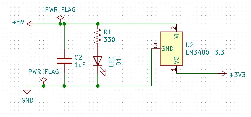
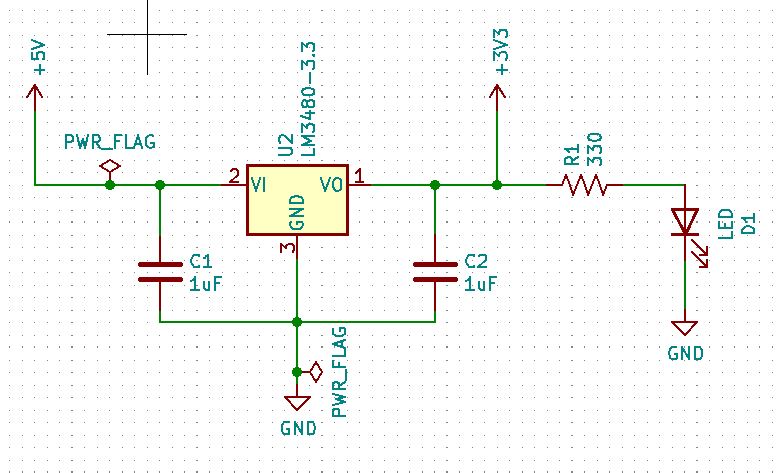
So on my schematic, the first two things I’ve added are the SAMD11C chip, and the 3.3v LDO (low drop-out) linear voltage regulator. The chip is an LM3840 3.3v regulator in a SOT23-3 package. This will convert 5v power to 3.3v to power the SAMD11C.
Next I’m going to add a capacitor to put in between the ground and the 3.3v line of the chip. This is just a simple power filter. You want to put it as close to the ground and power lines of the chip as possible.
And after this, because I know how to do it, I’ve added two LED’s and the two current limiting resistors for them (330 Ohm, though really, it’ll probably be 1k in use.)
And after this, as you can see in the above image, I’ve added the ADXL343 accelerometer. This has i2c and spi for communicating to the SAMD11C chip. It’s also in a QFN packaging.
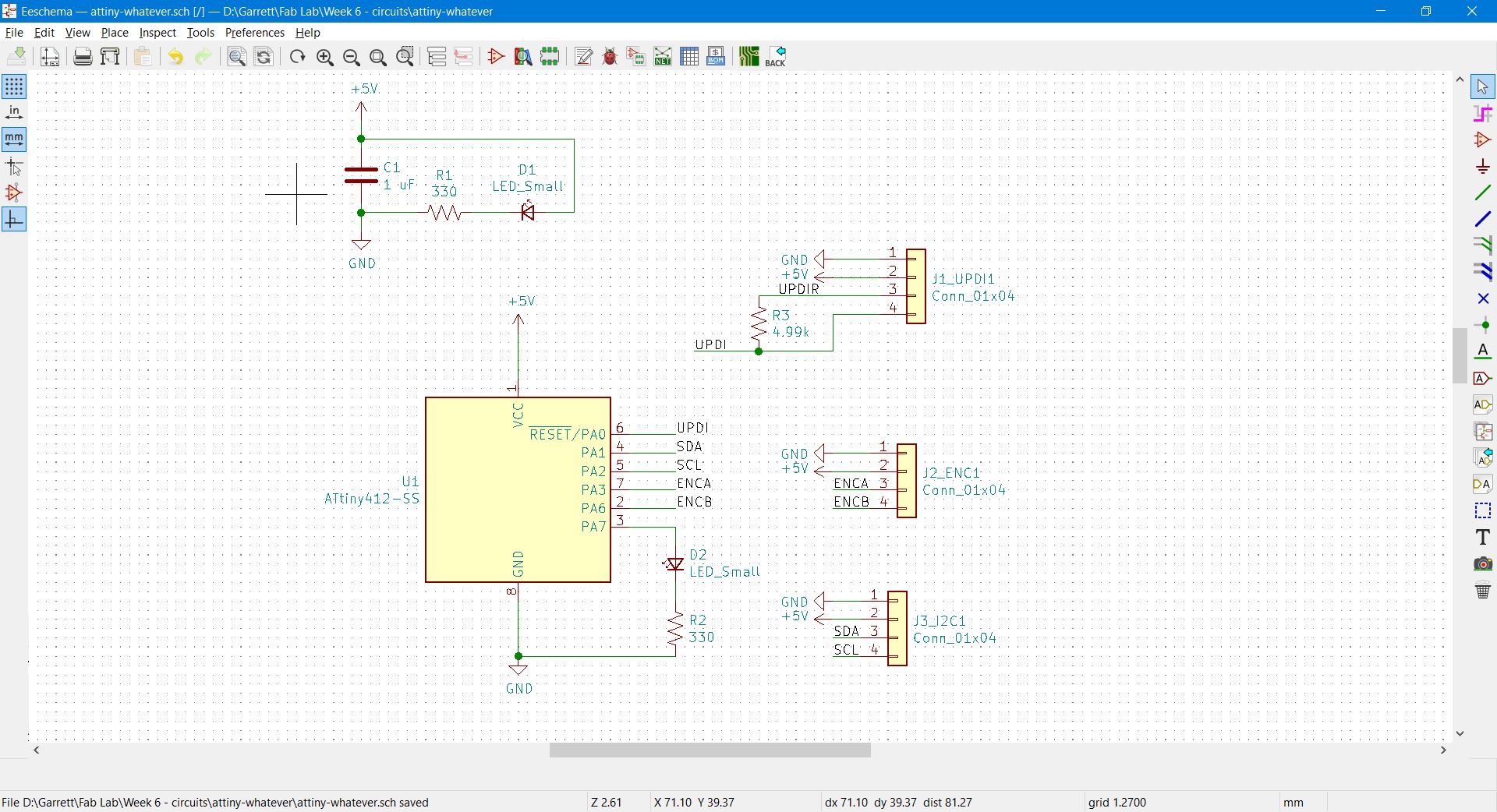
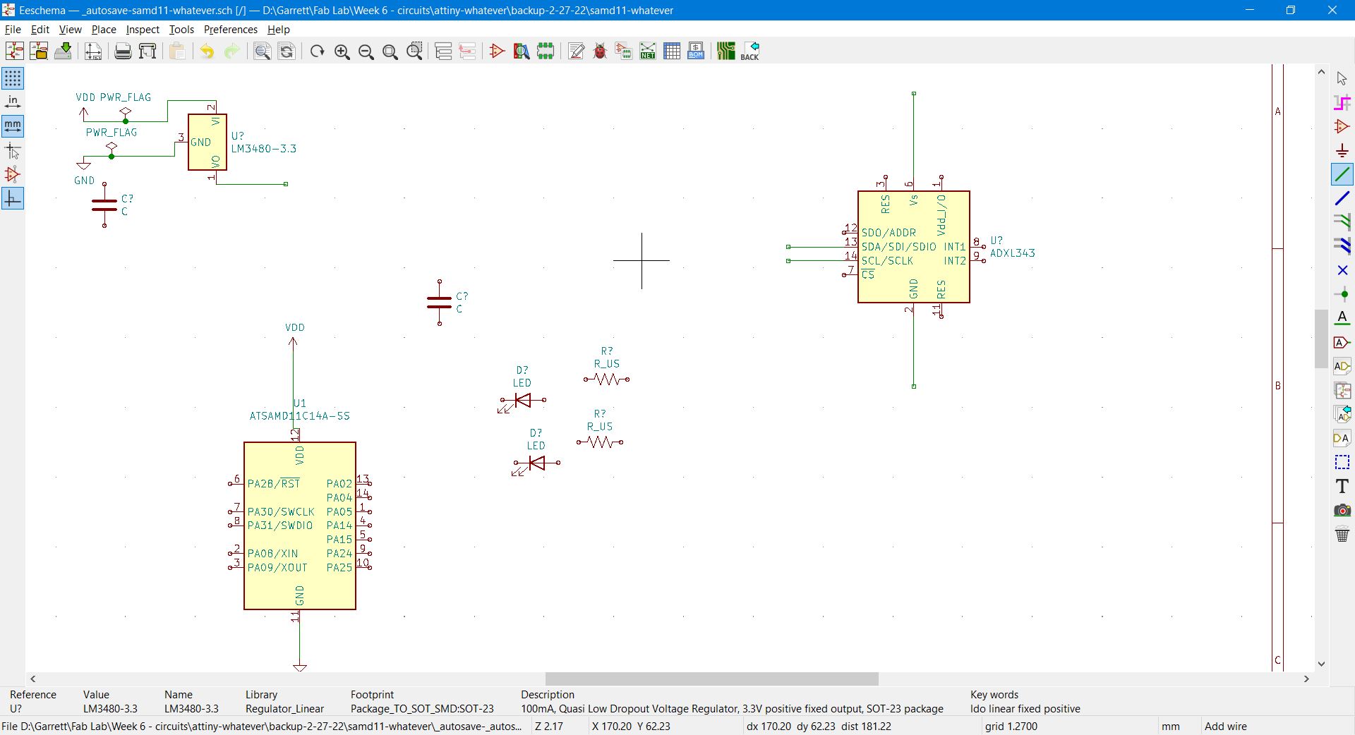
Creating a new Schematic in Kicad
To start with, you need to open a new project in Kicad. I’m using an older version of Kicad, but version 6 of Kicad is now out. When you first open Kicad, you’ll want to create a new project.
Kicad is a program that is made up of multiple sub programs. There is a one program to design a schematic, “eschema” and one program to design the PCB “pcbnew.”
First we want to open up a new schematic.
Notes and placing components, wires and labels in Kicad
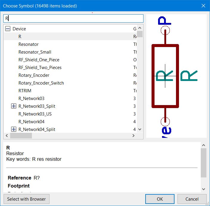
To add to the schematic, you’ll choose “place” and then place a “symbol.” (ie, the symbol for the part.)
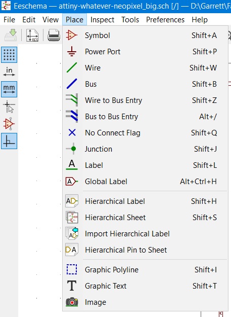
Shift + A is the hotkey that will also add a component to the board. Click where you want the component, choose the component, and then click on the schematic again to add it. You may need to do this multiple times, even if it’s the same component over and over again.
The below is what pops up once you’ve clicked on the schematic. You can search for what component you would like to place, choose “OK” and then place the symbol in the schematic.
You connect these symbols via “wires.” The wires can cross over each other. You’ll know they are connected if you see a green dot at the intersection of multiple wires. Shift + W is the hotkey for adding wires.
You also neeed to add power to your project. Much like the symbols, this is done by placing the “Power Port.” In my case, I included “5v” because the power was coming from USB or a 5v source. But then after a voltage regulator, it’s turned into 3.3v, which is designated by the power port as “3v3” Finally you’ll want to add GND. You can have mulitple power symbols in order to make the schematic cleaner and easier to follow. Shift + P is the hotkey for Power Port.
Which leads us to labels. If there are parts that aren’t immediately connected around the board (because it makes it conceptually easier, and a cleaner layout), you can use “labels” and just use the same label to connect multiple parts together. I very often do this, even when sometimes a part is next to another one, because later I need to move it around. Shift + L for labels.
I’ve also placed “No Connect Flag” on the pins of the SAMD11 and other IC’s that I’m not using. You don’t necessarily need to do this, but if you try the debugger, it will let you know. Shift + Q is the hotkey for No Connect Flags.
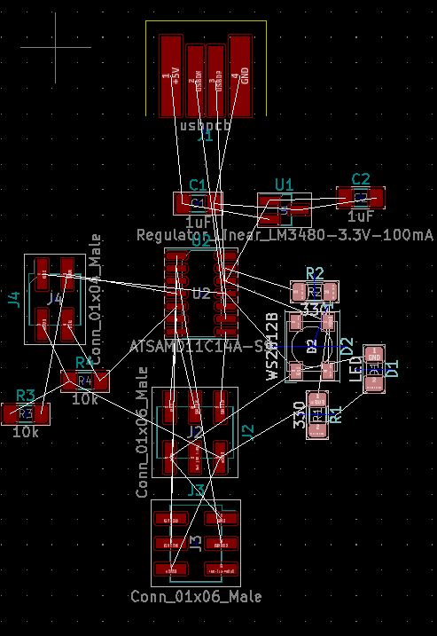
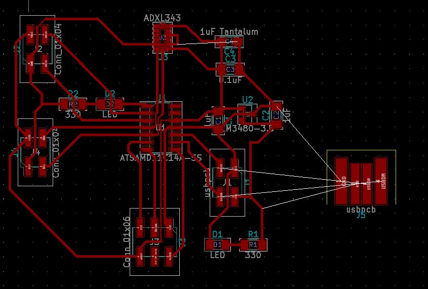
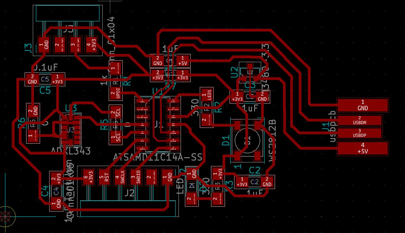
In the below image, you can see I placed a SAMD11C14 chip, a neopixel (WS2812B), a capcitor, a resistor, and then used labels “LED1” to connect the pin on the SAMD11C to the neopixel. I’ve also added the ground and the 3v3 power supply to the appropriate pins on the SAMD11C and the Neopixel.
![]()
When you start adding components, you’ll want to use the search function. You may also wish to use the fabacademy kicad library, though I’ve had problems with it.
Remember that “R” stands for a typical resistor and “C” stands for a typical capacitor. You may want to keep in mind what size and type of component you’re using, but for more generic parts, such as capacitors, resistors, leds, it doesn’t matter so much as we’ll add the actual values later. We will also add the footprints (the physical part that shows up on the PCB) later on as well.
At our lab, we’ll be using size 1206 smd components. Pin Headers are going to be 2.54mm pitch.
Starting to connect the dots
I’ve now connected the 5v power input and the ground to the Vin (input voltage - 5v) and ground of the LM3840 3.3v voltage regulator. From here, the 3.3v power (and FYI, for whatever reason, “3v3” is the correct power symbole to use.) will go to the SAMD11 and the ADXL343. For the Vout (output voltage - 3.3v) I’m creating a “power port” (from the “place” menu) and adding a 3v3 symbol (from Place -> Power Port) to the output. This symbol will then connect the power to the SAMD11C and the ADXL343.
I’ll add the 1uF capacitor closer to the IC for power filtering. (or maybe not. Learning as I go. You’ll see through this page, I’m constantly making edits and revisions. An expert I am not.)
I’ve updated it. Cleaned it up and added more proper labels. I’ve also added a power LED and current limiting resistor to the power input.
Later on I noticed Denny’s schematic for his board and copied his layout for the power bit.
Add Communications
I need to program this chip, and I need to connect the ADXL343 to the SAMD11C using the i2c bus.
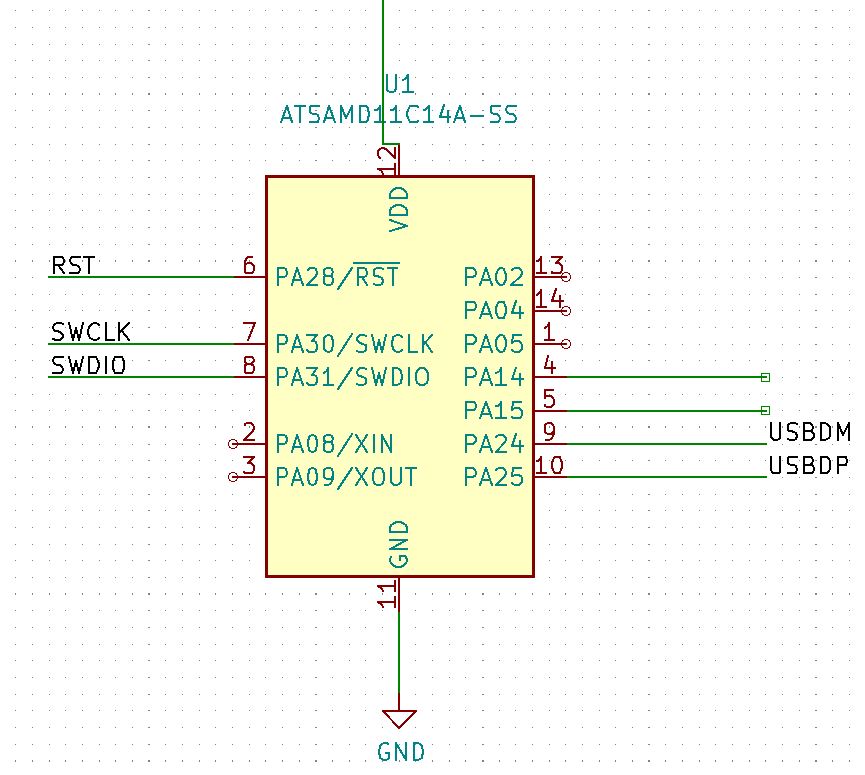
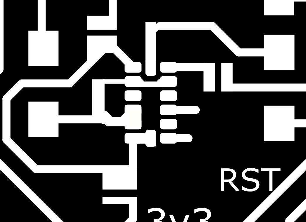
First I’m going to create a port to program the SAMD11C chip with. We can’t use UDPI to program the SAMD11C (at least as far as I’m aware.) So we’re going to use a JTAG to do it. This means we need to connect pins 6, 7, and 8 to a physical pin in order to program this chip. Pin 6 (PA28) is “reset”, pin 7 (PA30) is “SWCLK” and pin 8 (PA31) is “SWDIO”.
I’m also going to create connections for the USB data connections (though this may be temporary). I’m placing “labels” on the “wires” (all from the “Place” menu) to the SAMD11C pin outs. I’ve added a pin connector, and I’m also creating corresponding labels, for which the pins will be connecting. I’m connecting pins 9 (PA24) and 10 (PA25) to the future usb a pcb connector. 9 is USBDM, and 10 is USBDP. These are the data pins for the USB connector (Data Minus and Data Plus).
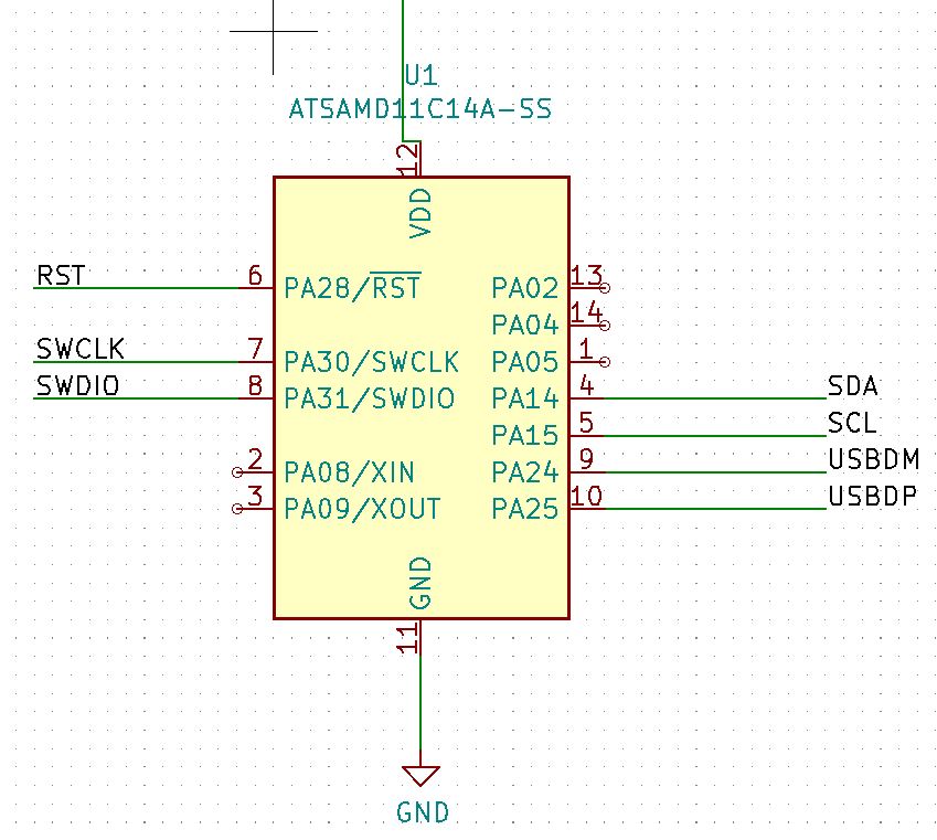
I then connect labels for the i2c. Pin 4 (PA14) for SDA and Pin 5 (PA15) for SCL.
The ADXL343 Accelerometer
Now this is something completely new to me. Not only is this a very difficult to solder part, but just trying to understand how it all connects took some time. I’m so used to connecting black wire to black wire, white wire to white wire, you take it for granted all the things it takes to make electronics work.
I read through the ADXL343 datasheet and found out the following…
ADXL343 Q’s and Notes
- What’s the difference between Vdd and Vs for ADXL343? It’s standby mode. It’s for power saving, but if you have multiple i2c devices on one bus, the chip needs to have power or it won’t be processing any i2c communications and it may interfere with other devices.
- Does Vs have to be connected? Yes, it and Vdd both need to be powered.
- Looking through the ADXL343 datasheet, The CS Pin needs to be tied to Vdd. The Alt Address pin needs to be tied to Vdd or Gnd, depending on what address you want.
- Do I need a crystal to use an ADXL343 effectively?
-
See page 16 of data sheet for information on i2c and address.
With CS tied high to VDD I/O, the ADXL343 is in I2C mode… … With the ALT ADDRESS pin high, the 7-bit I2C address for the device is 0x1D, followed by the R/W bit. This translates to 0x3A for a write and 0x3B for a read. An alternate I2C address of 0x53 (followed by the R/W bit) can be chosen by grounding the ALT ADDRESS pin (Pin 12). This translates to 0xA6 for a write and 0xA7 for a read
-
Says that pull up resistors are necessary for SDA and SCL i2c communications. Do I add these?
-
Page 26 says:
A 1 µF tantalum capacitor (CS) at VS and a 0.1 µF ceramic capacitor (CI/O) at VDD I/O placed close to the ADXL343 supply pins is recommended to adequately decouple the accelerometer from noise on the power supply. If additional decoupling is necessary, a resistor or ferrite bead, no larger than 100 Ω, in series with VS may be helpful. Additionally, increasing the bypass capacitance on VS to a 10 µF tantalum capacitor in parallel with a 0.1 µF ceramic capacitor may also improve noise.
-
ADXL232 wants 2.5v, but will work with 3.3v, but have increased accuracy errors. 3.3v it is.
Connecting the ADXL343
Reading all the above, this is what I was able to suss out and put together.
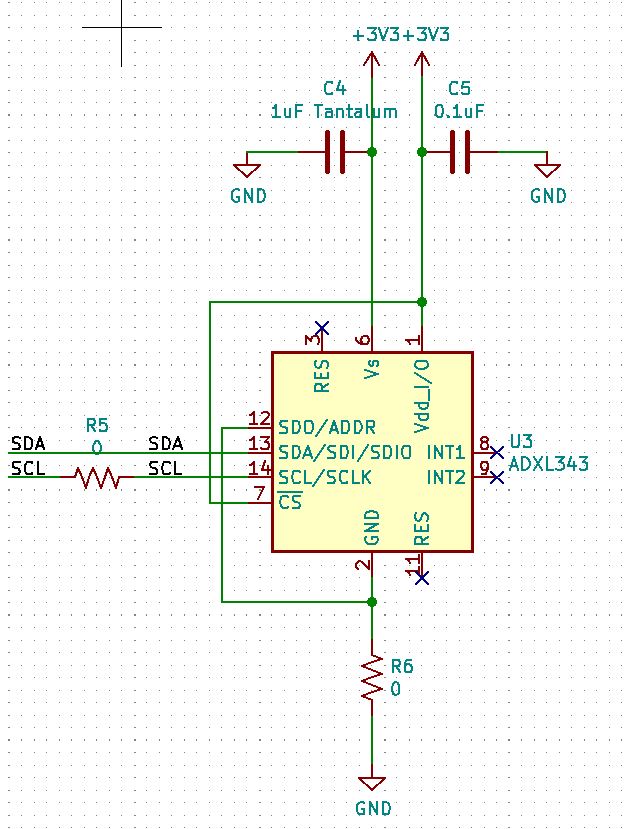
Both Vs and Vdd are connected to 3.3v, however the Vdd is connected to ground via a 0.1uF cap, and the Vs is connected to GND via a 1uF Tantalum capacitor. TANTALUM CAPACITORS ARE POLARIZED! (I should fix this on my schematic.)
I’ve connected Cs to Vdd, which enables i2c mode, that’s what we’re going to be using to communicate with the SAMD11C. (At this point, I don’t remember why I went this route over SPI.)
And Sdd/Adress pin is connected to GND, so the i2c address is 0x53. (I think I did this because it was easier to make traces to GND than it was too Vdd.) “This translates to 0xA6 for a write and 0xA7 for a read.” Whatever that means.
And you can see the labels for SDA and SCL, which will connect to the SAMD11C chip’s pins PA14 and PA15.
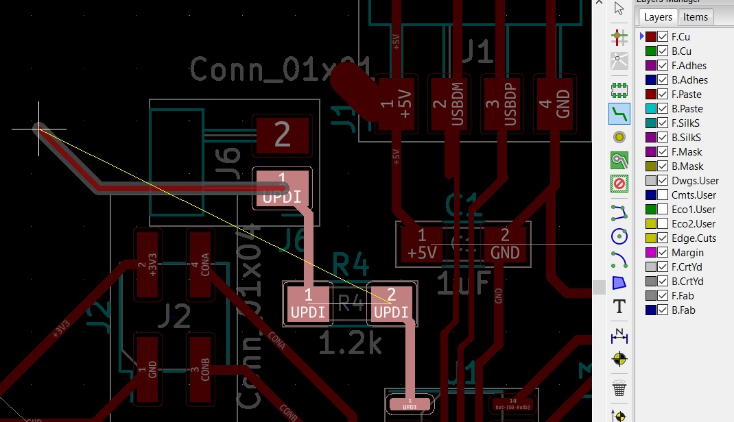
You’ll note there is a resistor on the SCL wire. This is a 0 ohm jumper that I needed because the way the pins are on the SAMD11 and the ADXL13 are opposite. So I need a jumper to allow the traces to cross one another.
NOTE: When using these type of 0 ohm resistor jumpers, you need to include a label before the resistor, and after the resistor as well.
I’ve added no connects to the un-used pins.
Movin On.
Let’s say that you’ve got your schematic already to go. Now we have to prepare it for turning it into a PCB.
There are a row of buttons at the top of Kicad’s screens that we’re going to use now.

From Left to Right:
- Annotate Schematic Symbols
- Perform Electrical Rules Check
- Assign PCB Footprints to schematic symbols
- Generate netlist
- Edit Symbol Fields
- Generate Bill of Materials
- Run Pcbnew to layout printed circuit board.
Annotate Schematic Buttons
This will turn all those labels that say “U?” and “R?” into “U1” and “R1”, “R2”, “R3” etc.
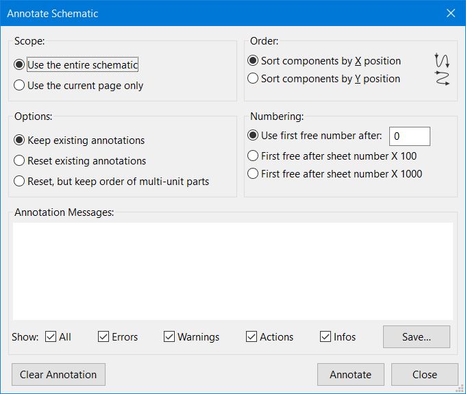
All you have to do is click the button, and then “Annotate” and “Close”.
You can also annotate all these labels as you go, but doubule clicking on the “R?” label symbols, as well as below them where it is the value label (it may simply have an “R” as default, but we would add something like “1k.” But if you don’t fill in the values, you can do this later; see below.
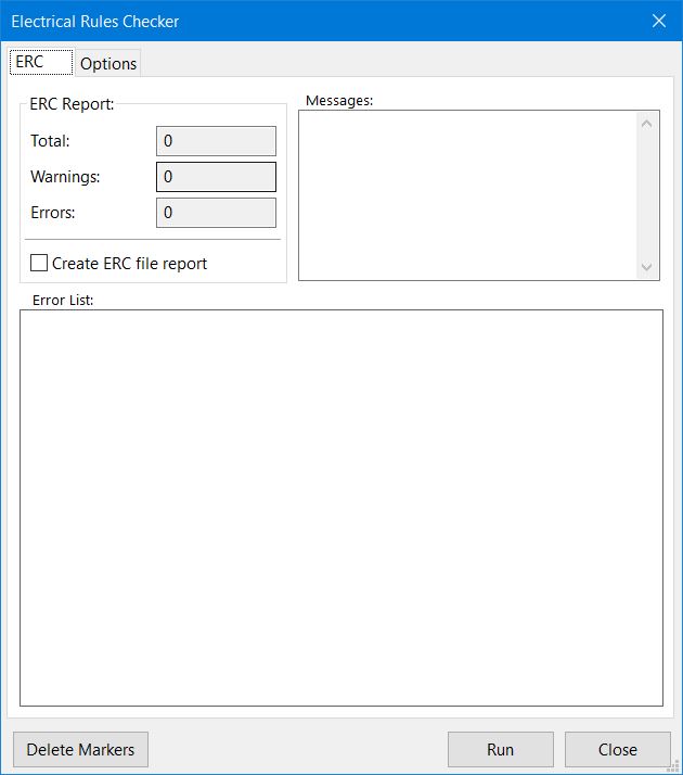
Perform Electrical Rules Check
This makes sure there are no obvious errors in your board. This isn’t going to stop you from making a bad board, but it will hopefully stop you from doing really dumb stuff. Maybe.
Again, just click the button. It may show you any errors, if there are any. It has errors and warnings. On the below image, I have one error. I believe it has to do with the way the GND is connected. I’m not quite sure, but I’m moving on. One of the nice things is that this shows arrows where the errors occur.
Assign PCB Footprints to schematic symbols
This is where we take the symbolic nature of the schematic and turn these symbols into physical spaces for the components to go. This is where you may wish to use the FabLab Kicad Footprint Library.
Generate netlist
This creates the interconnections between all the pieces that we’ll be using to actually create traces on the PCB itself. All you have to do is click the button and then save the file.
Edit Symbol Fields
This is where we assign actual values to our resistors and capacitors, and any other passive components if they need it. You can click on them and just assign the value. Don’t forget to note the arrow that you can click on and give different values for each resistor, capacitor, etc.
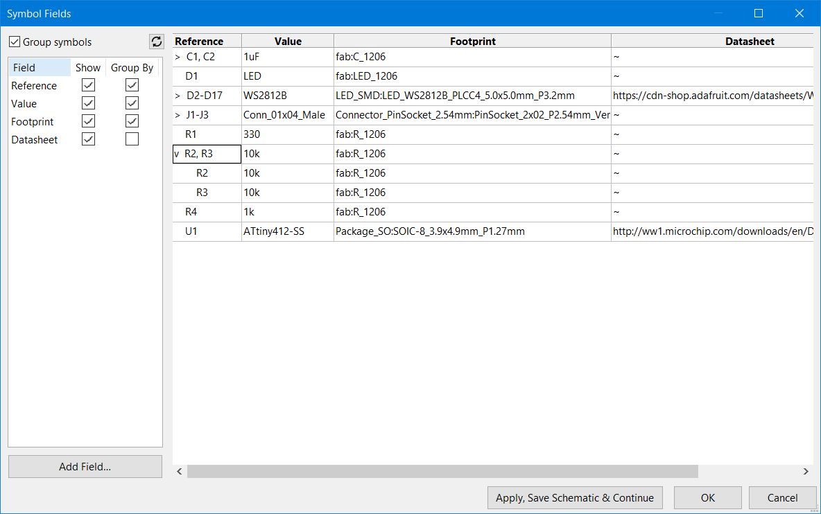
Click in the “Value” fied and simply type your value of the component. These values are simply notes, they can be just about whatever you would like them to be. But of course, it would behoove you to stick with industry standards. (And what are industry standards? I’d just recommend looking at other schematics and follow the pattern. Usually a 100 Ohm resistor is marked with a “100R”. A 100 kohm resistor will be “100k”. Capacitors will be marked in Farads. Either something like “1uF” or “1000pF”.).
The nice thing about doing this after assigning footprints, is that the footprints may have added values already for you.
Generate Bill of Materials
Haven’t used it. I’m using a small number of components. But if you want to print out a list of all the components that will be going on your board, especially to help order them, or collect them for soldering, this is where you would do it.
Run Pcbnew to layout printed circuit board.
After drawing the schematic:
- To give components names instead of “R? or “D?” go to “Tools” -> annotate schematic
- “Edit Symbol Fields” to give your components values.
- “Assign PCB footprints to Schematic Symbols” to give a pcb footprint and specific info on the part you are using. (Fablab has a basic library that may help with this: <>)
- Create “net list” - connects components for the pcb editor.
Then we save the net list and go to the pcb editor.
Open up the PCB Editor. Click here once you’ve done all of the above, and the PCBnew software will open up, and you’re ready to start designing your physical board.
KiCad PCB Editor
Some of the key buttons we’ll be using.

Here we must load the Netlist we just created, choose the file we just saved.
I used the mouse wheel to zoom in and out. Shift and mouse wheel pans the screen up and down. Ctrl + Mouse wheel pans left and right.
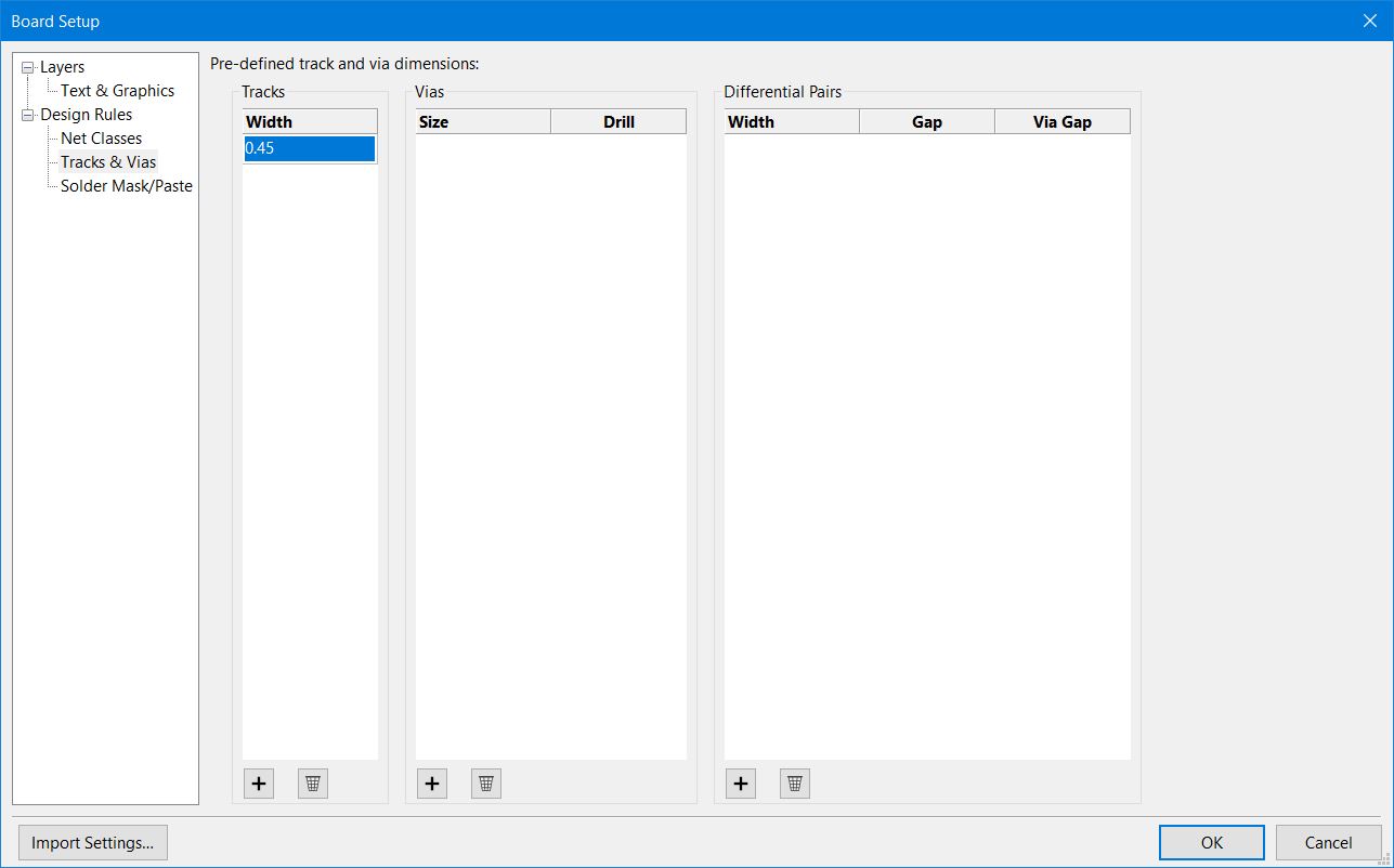
Change your Track sizes!
Remember to immediately change the size of your traces/tracks. If you’ve forgotten to do this, you can later go to “Edit” -> “Edit Track and VIA properties…” to change the size of your traces.
You may want to setup the board very quickly to help with some of the small stuff.
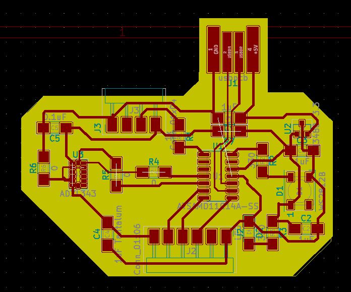
Now we route.
I’m not going to get too much in to the actual routing. Because I’m no expert, and it’s a pita. There’s got to be an easier/better way of doing it. But I don’t know what I’m doing. But if you love puzzles, you might find this part enjoyable. Because it’s just a giant maze of making the right lines go to the right spots. (And this is why we love double sided boards and vias.)
When we start, all of our components are nested right next to each other, all connected by a rats nest of white lines.
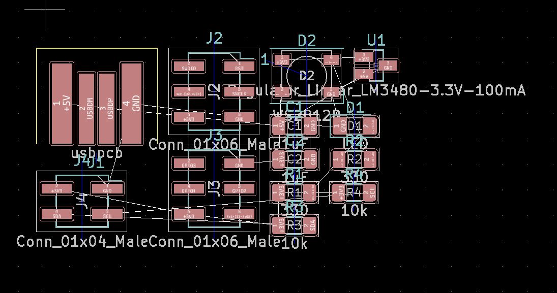
Our first job is to clean this up, and using the “Move” and “rotate” commands, seperate the components and start putting them into some sort of functional and logical system, where we can route the necessary traces to where they need to go.
Then, click the “Route Tracks” tool on the right side of the screen, making sure that you are in the “F.Cu” layer (it has the “>” next to it, and you should be by default.)
When we start routing tracks, you’ll see the “ghost lines”/”rats nest” connecting all the parts. This gives us a good idea what needs to connect to each other. Click on one of the components that we wish to connect, and you’ll see that the other components to which it can be connected are highlighted.
Now connect the two pieces with a trace, and click, and you’ve connected them.
You just have too connect all the other components on your board, without crossing the traces.
But you create tracks on the F.Cu layer and connect the pads to the corresponding pad. When you start, Kicad highlights what pads need to be connected. It’s also impossible to accidently connect the wrong pads.
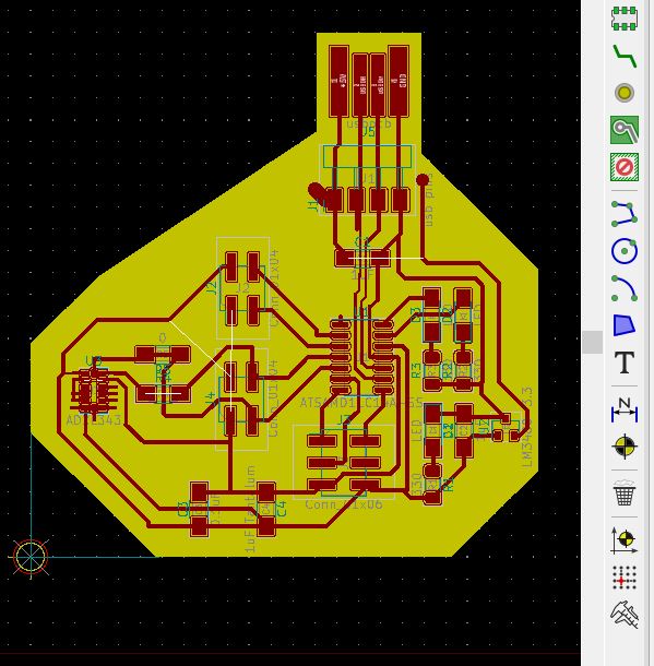
Draw the board outline
Click on Eco2User on the right of the screen. Then you can choose the polygon tool, and draw a box around the board. This is what will be plotted and milled out.
Set the origin
There are two origins buttons, I don’t know if it’s necessary, but I do both of them.
I set the origin at the bottom left of the PCB.
Export the Board
Getting the board ready to mill.
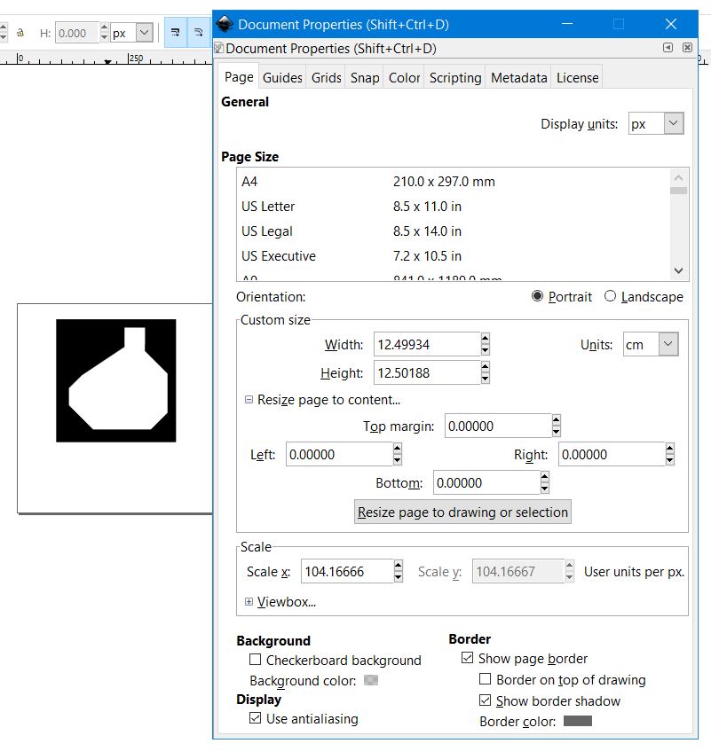
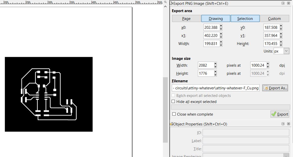
Note: You may need to click on the “Export Area” from Drawing to Page, or back again, to get it to register the correct size. I’ve had this problem a couple of times.
BOM - work in progress
This is constantly changing
| Designator | Component | Info/Notes |
|---|---|---|
| U1 | SAMD11C14 | |
| C1,C2 | 1uF 1206 | |
| C3 | 0.1uF | for adxl232 |
| C4 | 1uF | Tantalum, for adxl232 |
| D1, D2 | Red or Green LED 1206 | |
| LED1 | Neopixel WS2812B | |
| R1, R2 | 330 ohm 1206 | |
| U2 | 3.3v LDO reg | SOT23-3 package |
| U3 | ADXL 343 accelerometer | QFN package data sheet |
SAMD11C Q’s and Notes
- Can I use the programming pins (RST (PA28), SWDCLK (PA30), SWDIO (PA31)) for other uses if I don’t need to program the chip?
USB PCB Footprint
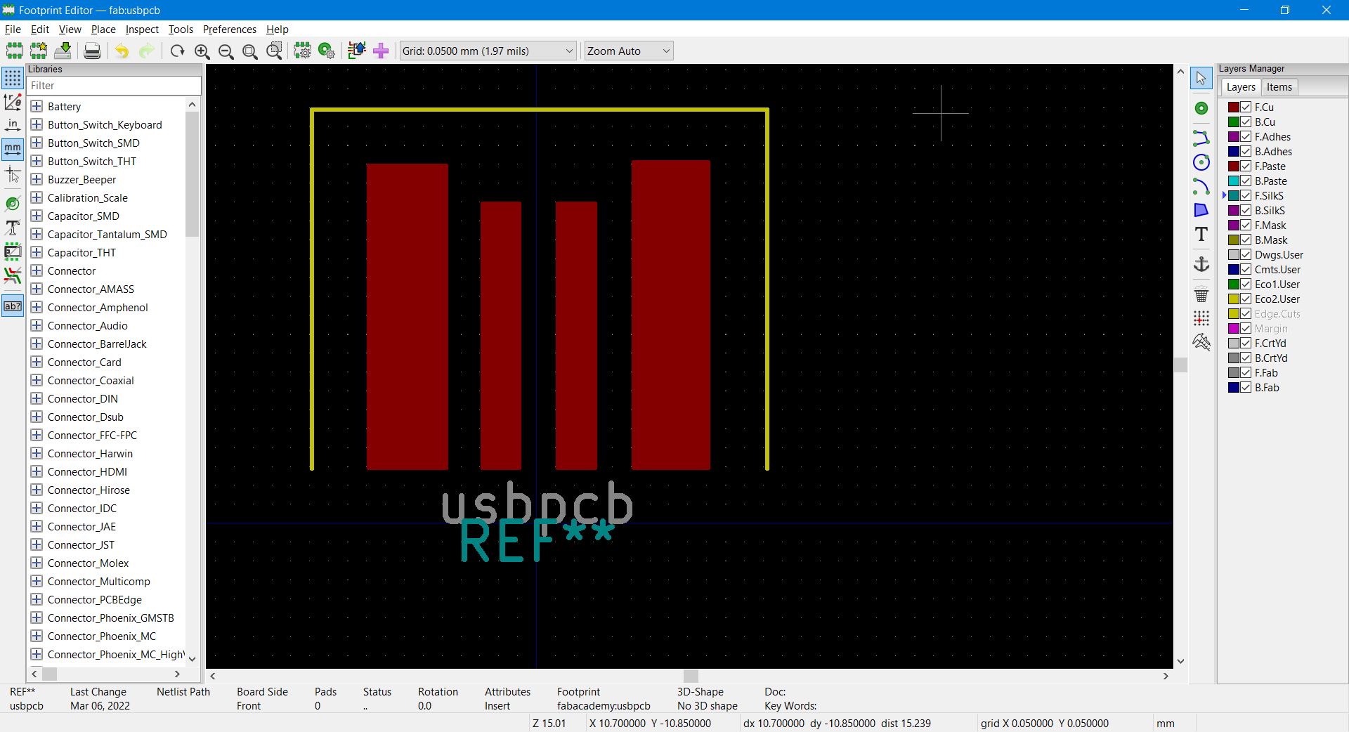
Garrett’s USB PCB Edge Connector footprint for Kicad
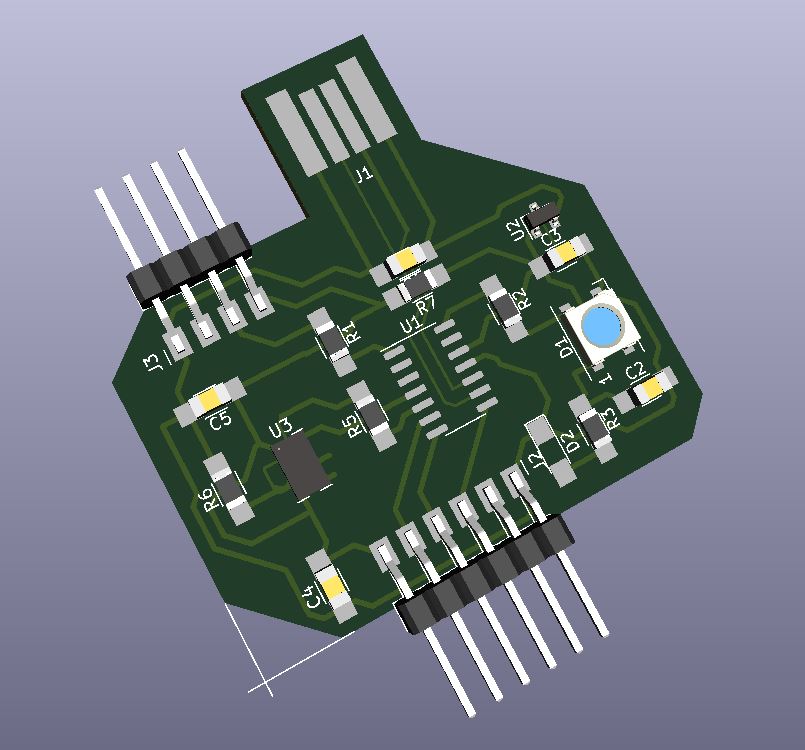
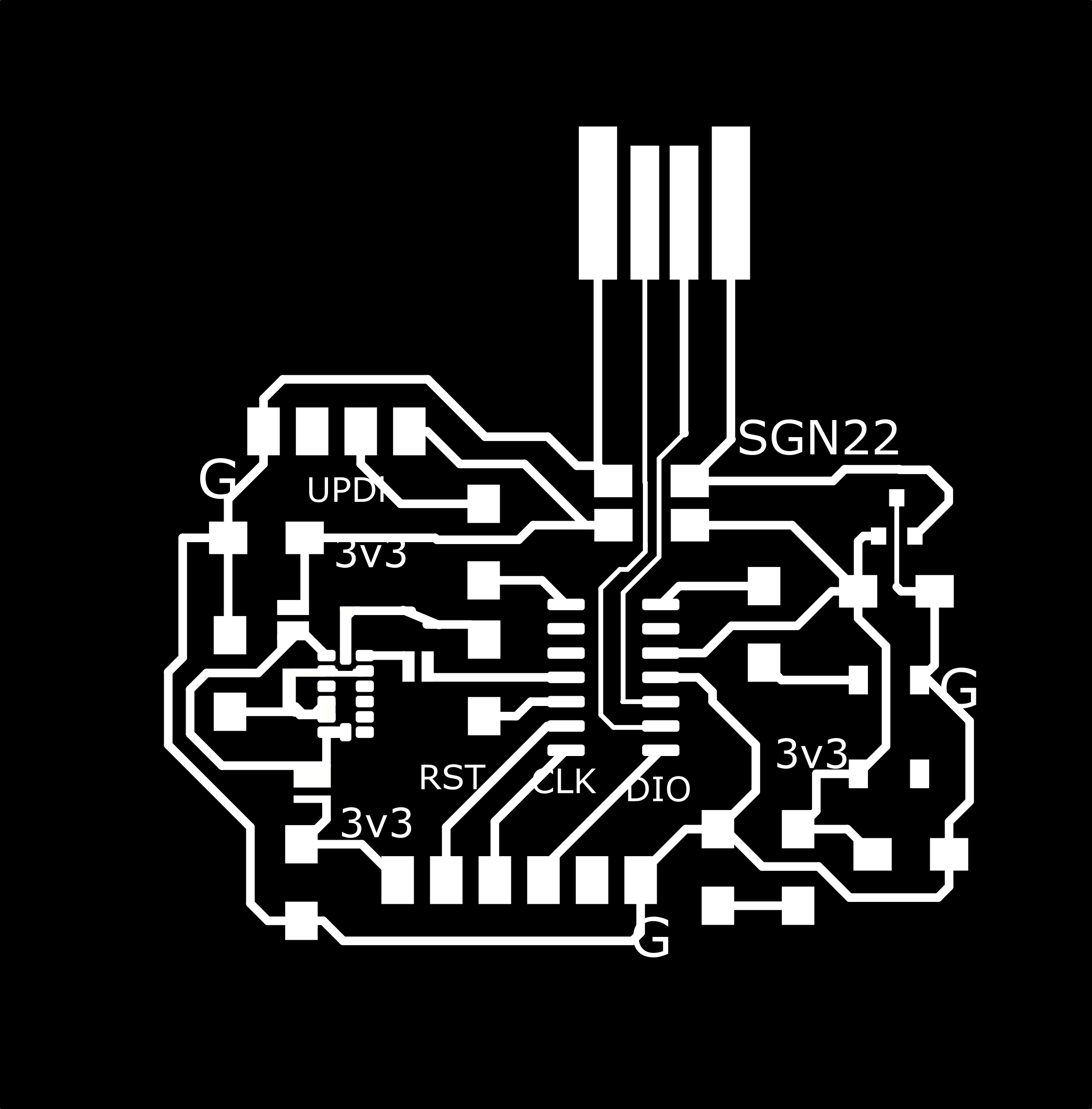
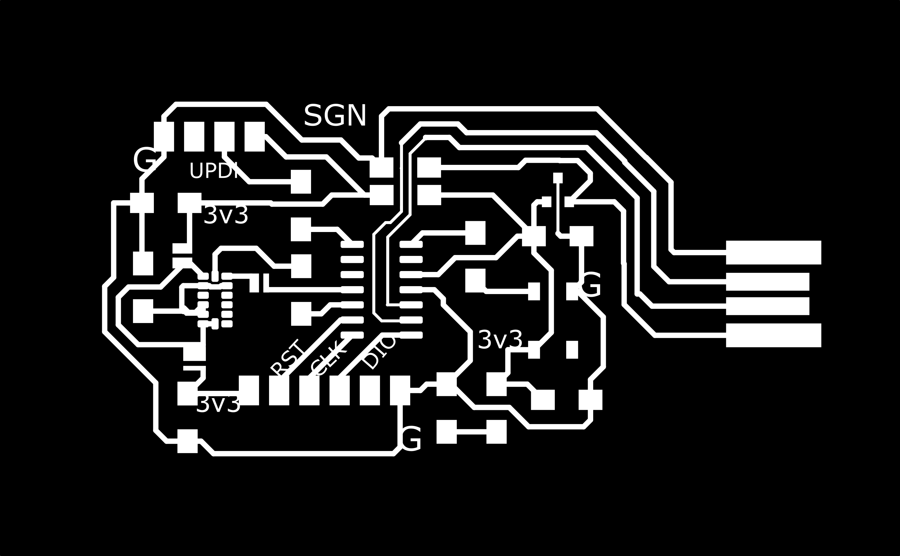
Current State of SAMD11C Board
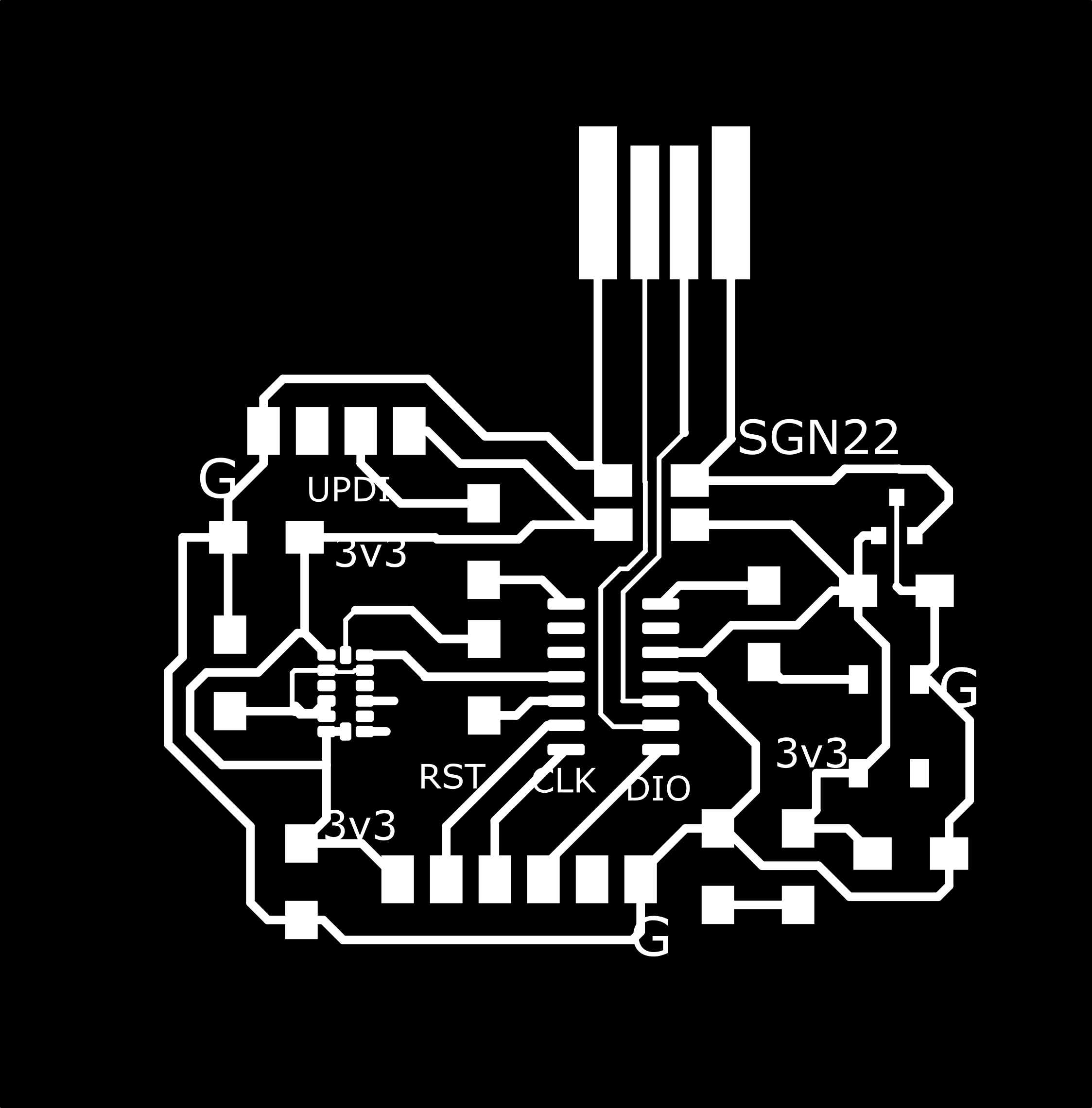

3d render - missing another IC. The 4 pin SMD pins out the front won’t be there.
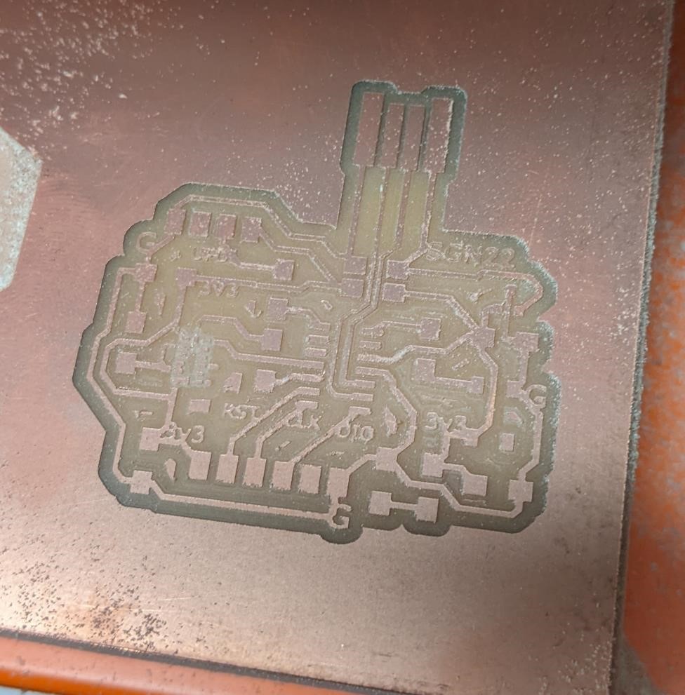
Milled Board:
For Laser cut solder past stencils (thin red lines don’t show up well on this background.)


Creating a board and soldering a QFN ADXL343 Chip
REST Milling
REST milling is a machining/CAM procedure to use the largest tool as possible to take as much material off as fast as possible, and then go back and clean up the areas that the large tool couldn’t go with a smaller tool. It’s faster (and thus cheaper), better on tool life.
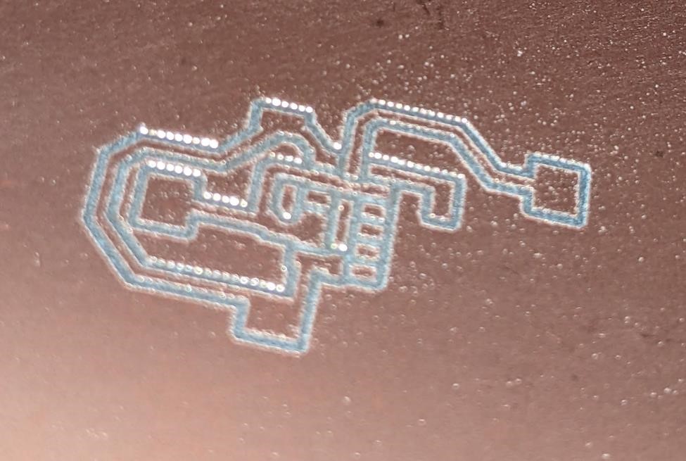
I wanted to do this in order to cut the tiny pads that ADXL343 will need, as a 1/64” bit is too large to fit inbetween the pads and cut them. But I also don’t want to wait the ridiculous amount of time it’d take to cut the board with a 0.100mm (0.004”) v-bit.

Tried my REST milling technique. I .. Uh.. Forgot about something… But it’s a work in progress. I didn’t exactly expect this to be a success.
I tried using a v-bit, which supposedly has a 0.100mm (0.004”) tip. I sank it down 0.005”, which in retrospect was too deep. I’m going to have to experiment (or do the trig, but I wasn’t sure what the angle on this v-bit actually was, there was no info about it.) in order to get the right width of cut. I’m also going to have to figure out how to do a proper REST milling without cutting all the traces. (Or I may not worry about it, but have the traces extend at least 8mm or more from the pads, and then just make solder bridges. But I’m not cutting an entire PCB with a 0.005” bit.)
And then the laser cut solder stencils… I need to shrink the small pads for the ADXL due to the laser’s kerf.
v2 of the laser stencil:

How are we going to solder that QFN chip?
However, it’s also a “flat pack” or QFN package, which means it doesn’t have any pins/leads to solder too that are accessible from the side of the chip. You have to use hot air or reflow ovens and solder paste in order to solder these components. This is going to be very tricky, since I don’t exactly have access to either.
What makes soldering this even more difficult is that you can’t just apply solder paste liberally to the board (and doubly so for un-varnished pcb’s I’m assuming), but rather the paste needs to be applied just in the specific pads to help avoid solder bridges.
Generally you use a stencil to help with the application of the paste. With Adam Harris’ help, we’re planning on using the laser cutter to cut a stencil out of kapton tape, apply the paste to the board using this stencil, and then use hot air to melt the solder paste and solder the chip to the board.
Not having a real hot air station is going to make this more difficult. You would normally use the stencil for every component on the board, gently place the components and then use a reflow oven to melt all the solder at once, which using surface tension tends to suck the components down creating a finished board.
But since we don’t have a real hot air station or reflow oven, my plan is to use a big old fashioned hot air gun (think hotter blow dryer) and solder paste to solder the chip, and then just hand solder the rest of the chips onto the board. We’ll see how the experiment of cutting a stencil with kapton tape, solder paste and a hot air gun works.
I was planning on making the footprint pads of the ADXL343 much longer, and this would hopefully help conduct heat to the solder paste to allow it to work.
But using the below reflow station would be the best way of doing this.
(notes: this “pre-heating station” that Neil showed us would be cool to try. )
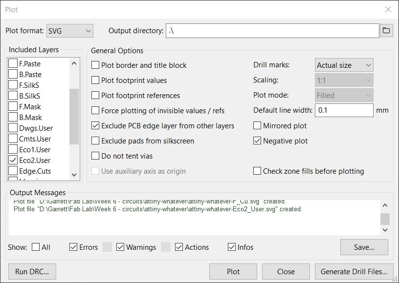
I found that exporting a SVG via Plot in Kicad makes it very easy to select the traces within Inkscape, delete them, and then change the pads to a stroke weight of 0.1pt and the color red, in order to laser cut them in Kapton tape.
I’ve cut the pads in some thin kapton tape I had laying around, and while not the best use for an actual stencil (though it’d probably work), it was good enough for testing.
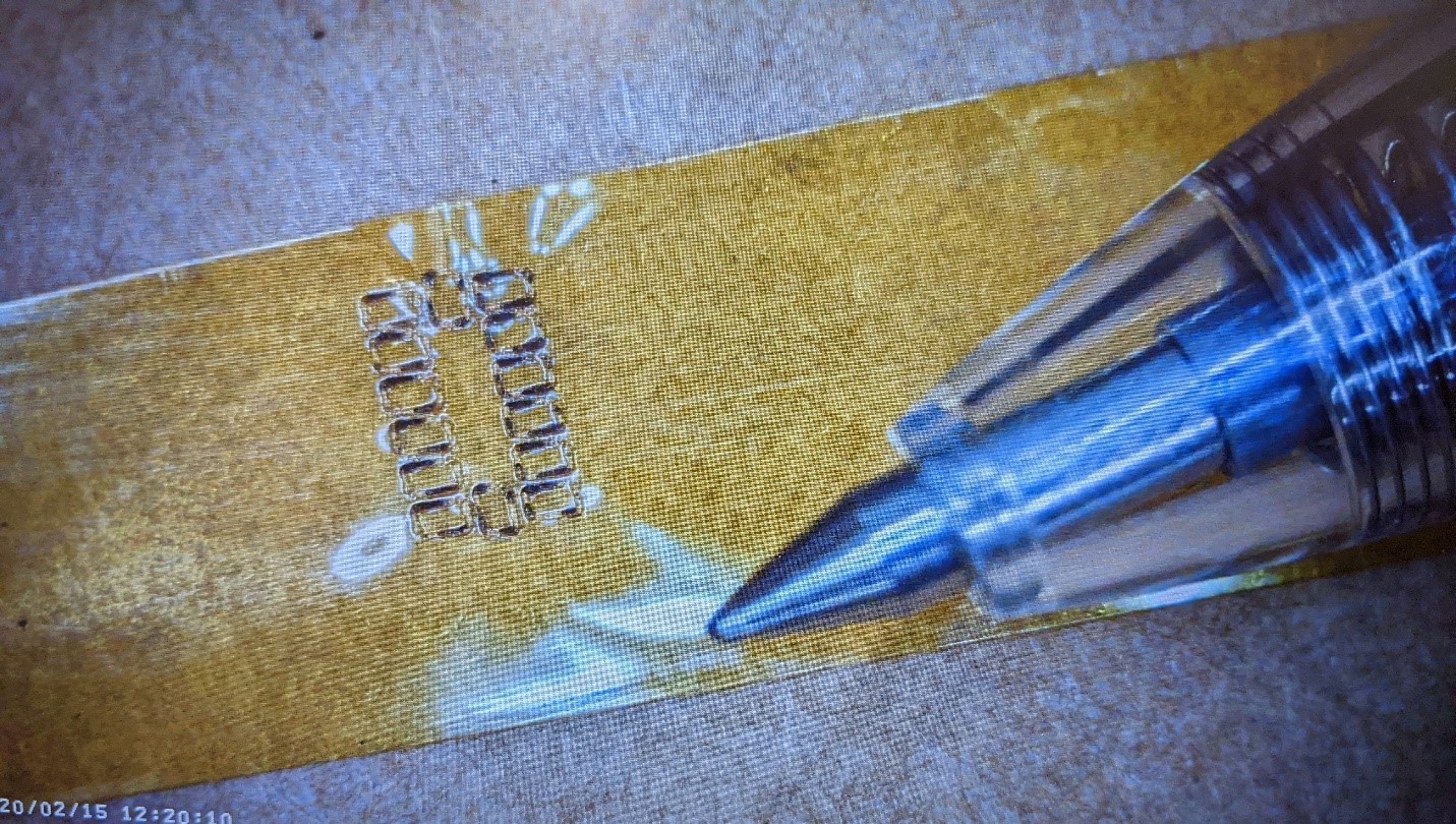
My first few tries, the power was a bit off:
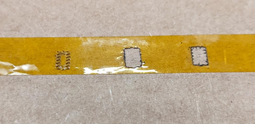
But I was finally able to get it to cut well. The trick was to use a speed of 100% and a power setting of 6%. The other trick is to separate the actual pads from the outside stencil. For this, I used a very sharp, fine exacto blade knife to help lift the pads from the paper. But this was only somewhate succesful. After I helped seperate the pads with the knife, I used masking tape, put it on the kapton tape, and was then able to lift off the inner pads with the masking tape.
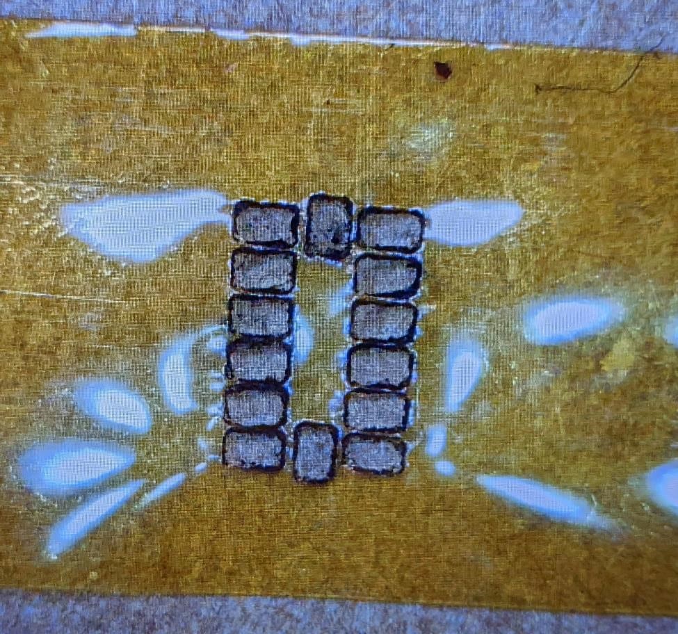
Because of the laser kerf, I’ve shrank the pad size by about 10% and I’m going to recut the stencils.
v2 of the Rest Milling PNG
For version two of the “REST” milling, I’ve created breaks in certain solder pads, so the small endmill will cut these out, but then I can go back and create solder bridges to reconnect them.
And the PNG Files:


And the results from the second attempt at rest milling came out much better.
V4 of the above SAMD11C and ADXL343 Board.
DON’T USE THIS BOARD!!!
I switched the 5v and GND of the USB plug. This board is not to be used. I’m leaving it up just because, but please don’t use this. It won’t work.
Hopefully get to try soldering it soon. Just need a hot plate/hot air reflow station.


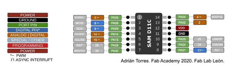
The pinout for the SAMD11C
Attiny Board v3 - Still making changes and working on these things.
New Attiny design with a neopixel.
Neopixel used is a WS2812B.
The pinout of the neopixel is below. Note that VSS is the same as GND.
![]()
![]()
![]()
![]()
![]()
Files
As is often the case, the full files are large, and in this case are unnecessary. The above data should provide enough data to mill the work, or be able to quickly recreate the work. If you wish the actual kicad files, please let me know.
Group Work this week - Electronics Development
You can find our group project here for now: Unit 7 Group Project
I helped turn on an Oscilloscope. I was able to get the alligator clip to actually stay on the tiny little arm on the board. I twisted the dials, and probed the circuit until I got the Oscilloscope to move. We managed to see the led blink on an off, with the voltage increasing and decreasing as the led blinked.
Trust me, that’s a win.
You shouldn’t let people like me play with electricity.
However, later I came back with someone who knows what they were doing, and I learned a lot more.
With the group project, we worked on learning how to properly use an oscilloscope, as well as “reading” what is going on with parts of the boards.
I learned how to actually use an oscilloscope (and that you’re supposed to calibrate the oscilloscope leads when you first use it.) and the different features on newer oscilloscopes (such as how to use the auto-trigger.)
I helped with testing out different boards, focusing on the boards with neopixels.
I learned that with just an oscilloscope you can see the serial data of the neopixel as it moves from neopixel to neopixel, only transferring the data necessary for the rest of the neopixels.
I also started to learn how to find and trace shorts in my boards, however, this is still very much a work in progress.
And always, I learned that there’s a lot more I need to learn.
Resources and References:
Great Kicad tutorial for fablab: http://fablabkamakura.fabcloud.io/FabAcademy/support-documents/microcontrollers/KiCad_tutorial/
Yep: https://www.didel.com/SamProject.pdf
Stefan Wagner’s SAMD11C development board was very helpful https://easyeda.com/wagiminator/samd11c-development-board
This was a helpful kicad tutorial: http://babryce.com/kicad/tutorial.html
https://forum.kicad.info/t/errtype-3-pin-connected-to-some-others-pins-but-no-pin-to-drive-it/10946
https://ww1.microchip.com/downloads/en/DeviceDoc/ATtiny212-214-412-414-416-DataSheet-DS40002287A.pdf
- page 559
https://www.youtube.com/watch?v=l9b_6WLemmg
http://sheekgeek.org/2020/adamsheekgeek/attiny412-general-purpose-blinky-board-and-updi-programming
https://fabacademy.org/2020/labs/oulu/students/achille-gakwaya/assignments/week07/
https://fabacademy.org/2020/labs/oulu/students/achille-gakwaya/assignments/week09/
https://fabacademy.org/2020/labs/oulu/students/noora-nyberg/assignments/week09/
Adrian gave me some inspiration: https://fabacademy.org/2020/labs/leon/students/adrian-torres/samdino.html
https://www.reddit.com/r/AskElectronics/comments/8g21wf/what_is_the_difference_between_scl_and_sck/
http://www.bitbanging.space/posts/attiny-1-series-i2c-library
If I did this more often, I would use this: https://github.com/openscopeproject/InteractiveHtmlBom
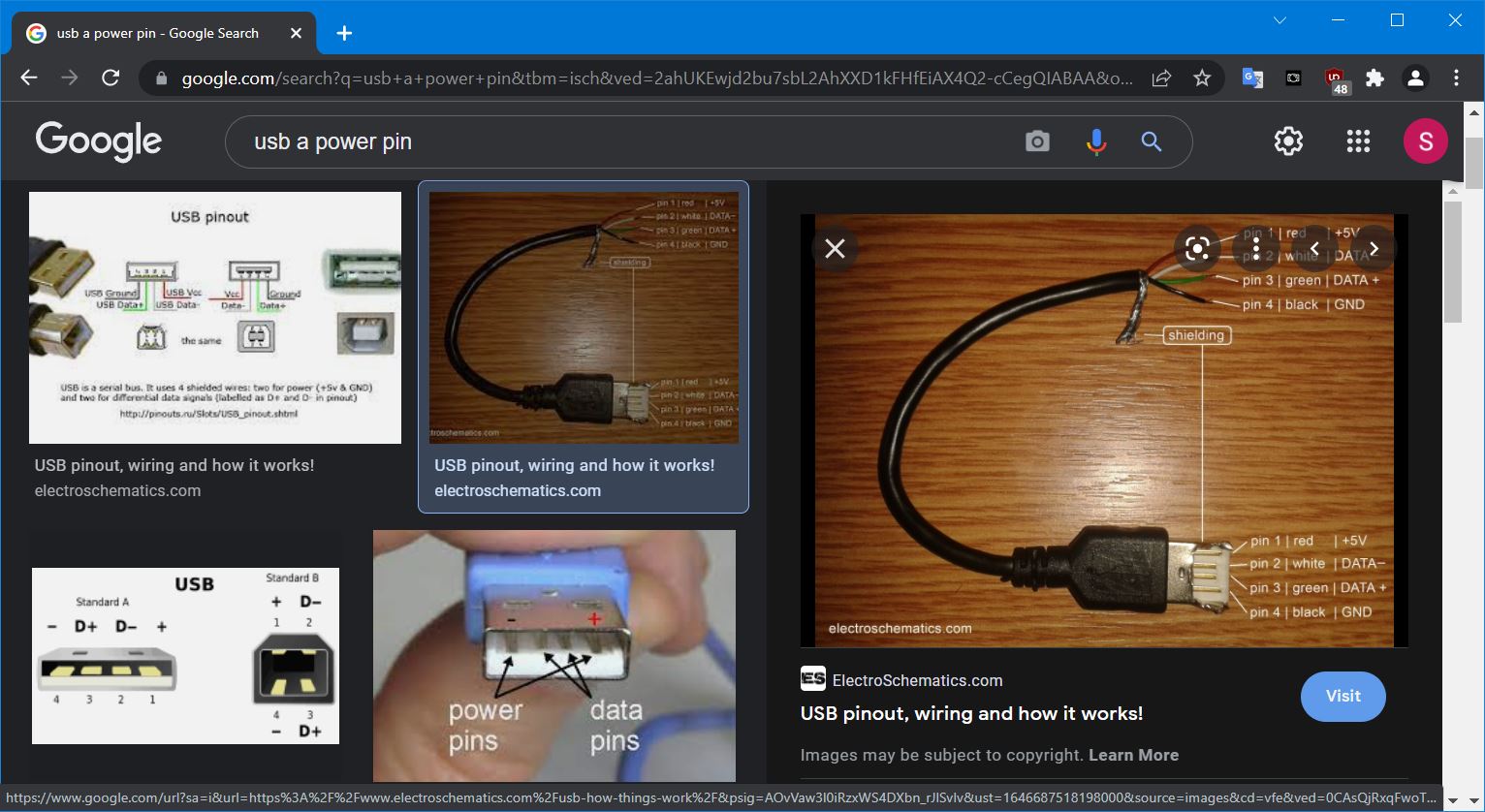
USB PCB Pins
Google helped me figure out how to arrange the usb pcb pads. That would be bad to get wrong.