
Assignment 5 - Electronics Production
Assignments
Group Assignment
- characterize the design rules for your in-house PCB production process
- extra credit: send a PCB out to a board house
Individual Assignment
- make an in-circuit programmer that includes a microcontroller
- extra credit: customize the design
- mill and stuff the PCB
- test it to verify that it works
- extra credit: try other PCB processes
Individual Contribution to the Group Assignment and Link to the Group Assignment Page
The Group Assignment Page for the Lab in Kamp Lintfort can be found here.
For this Group Assignemnt I went through the whole process of creating the Line Test from the Lecture on our milling machine, the Roland MDX-40. I created Toolpaths with Mods, prepared the copperplate, set the X/Y/Z-origin and the rest of the settings accordingly and cut the piece. So I learned the whole process from image to cutting with our machine in the Lab with this Group Assignment.
Making the In-Circuit Programmer
Design
At our local lecture we got recommended one of two designs for our first In-Circuit-Programmer. One design consisted out of two seperate boards and the other board was just one part and had a UPDI mode aswell as a FTDI mode between which the user can switch using a jumper between three pins. While the board design of the board that only consisted of one part seemed more complex, I still chose it because I liked the thought of multiple functionalities between which the user could switch. The board was developed by Ahmed Abdellatif, one of our instructors whom also helped me greatly to finish this assignment as I had no Idea of this topic and never worked with the machines needed for this assignment. A description of the board and the needed files to create it can be found here.
Instead of using the design as is, I asked Ahmed if he could show me how to change the boards design, which he did. He gave me access to the KiCAD project of the board where I could the change stuff around. Doing this for the first time, the schematic of the board was quite intimidating as I still dont really understand all of the parts and why they are there. But with the help of Ahmed I could begin changing the design of the board to the one I imagined. After downlaoding KiCAD and loading up the KiCAD project, the first thing I had to do was create the new outline of the PCB.
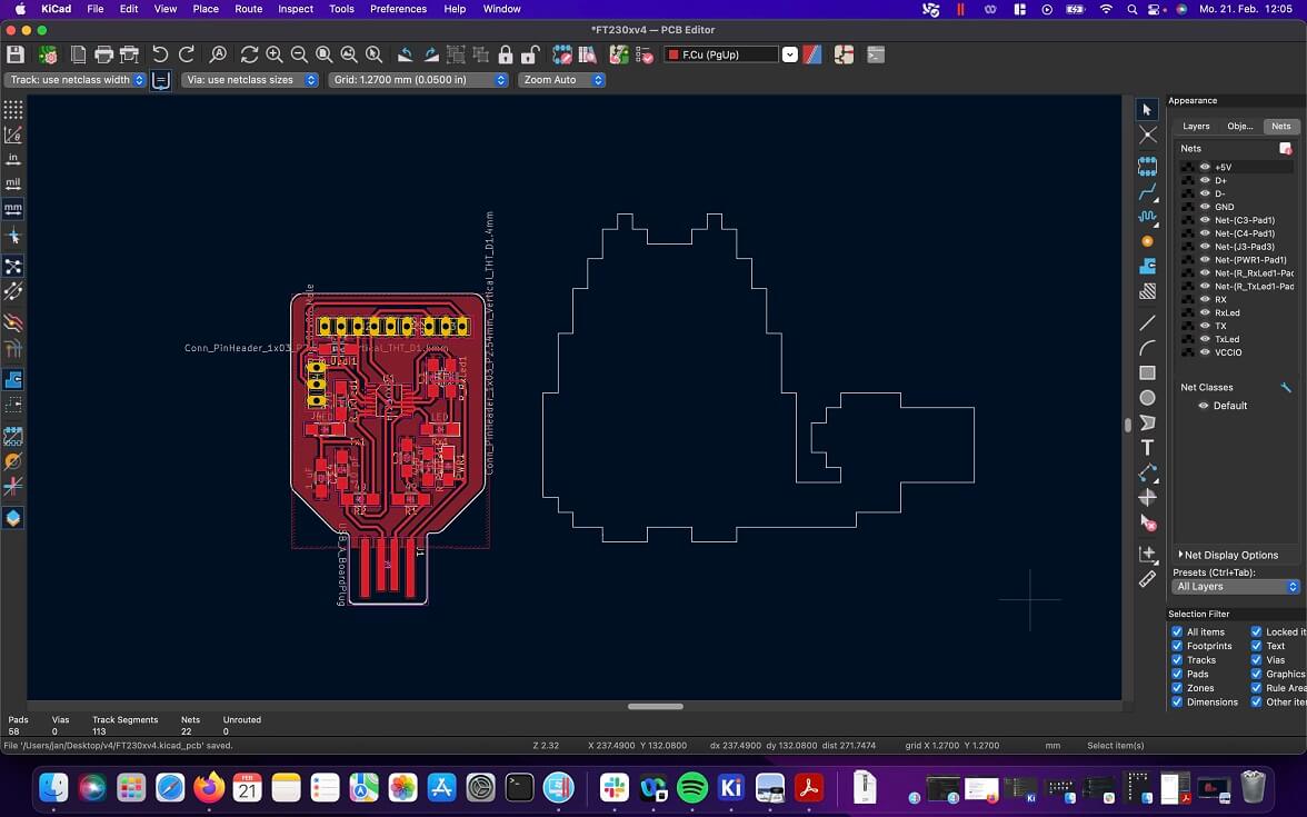
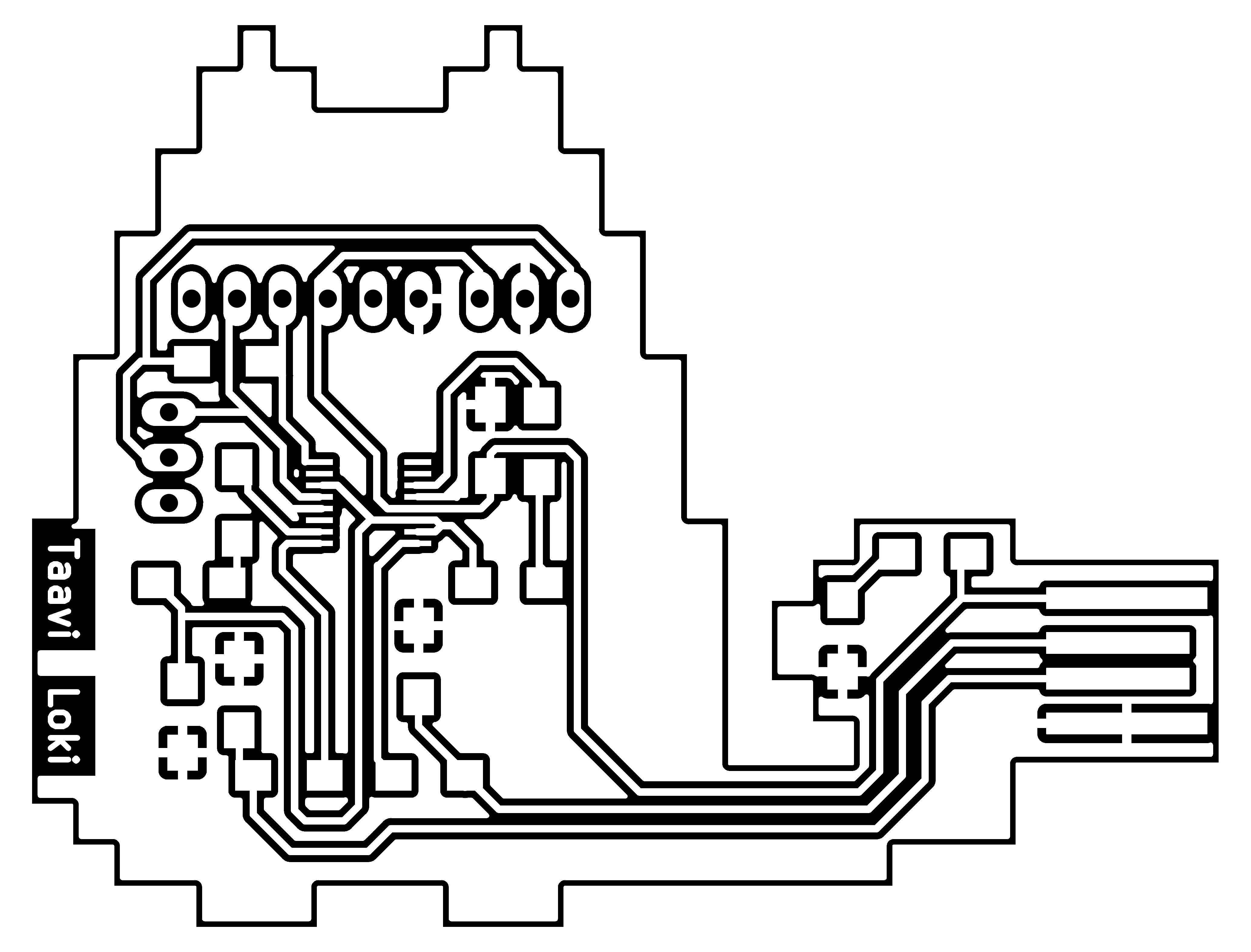
To create the outline shpae of the new PCB-design I used inkscape. My idea was to use the cat logo/ cat sticker from my first two weeks to create a pixelated cat shape PCB. I loaded the cat logo into inkscape and simply traced the bitmap to get the svg of the outer shape. The svg was then loaded into KiCAD resulting in the following:
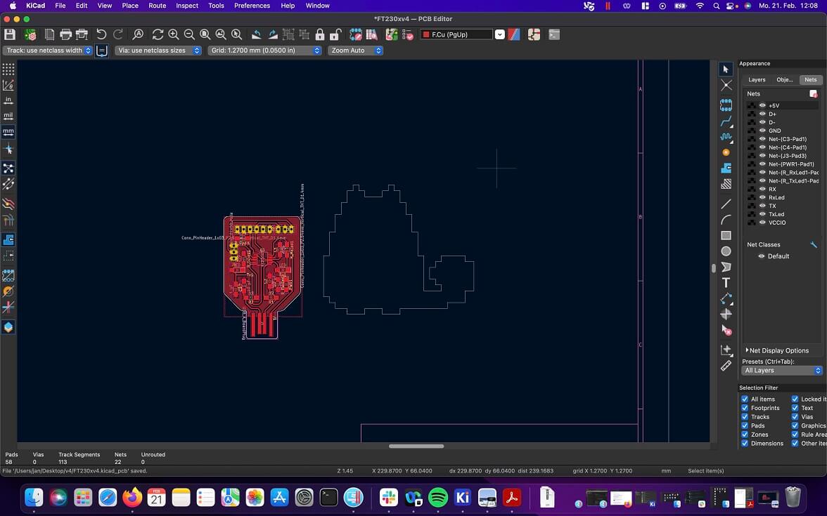
Ahmed then showed me how to move stuff around in KiCAD and how to use the most important featrues of the programm. My idea shifted around a little bit after seeing the image of the cat next to the pcb design of Ahmed and I had the idea, that the cats tail could be used as the USB port of the board which I found quite funny and would greatly change the original design to something personal. Within KiCAD you can drag around the different nodes of imported svgs. So after changing up the cats svg a little bit i was left with this:
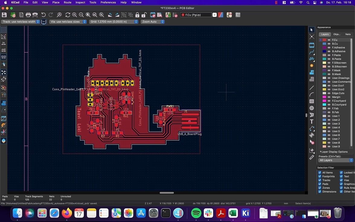
With a new idea in mind I started to change up the old design by first moving the USB-A port to the cats Tail. After deleting all loose traces I then moved everything else to the main part of the cat, deleting the old outline in the process. The next idea was to change the power LEDs position to the tail aswell to create some space on the main part of the cat. After moving the needed parts, I just reconnected the missing traces the right ways and thought I was done. Ahmed then told me to look out for the traces around the Tail, as they were too close to the outer edge, not allowing the ground layer to revolve around the whole PCB. After fixing this and also adding the names of my two cats onto the board, I was presented with the following design for my PCB:
There are a few other ideas I had in mind, but they would have changed the board design so severly that I would have lost too much time. So I moved these changes to a potential V2 of this board.
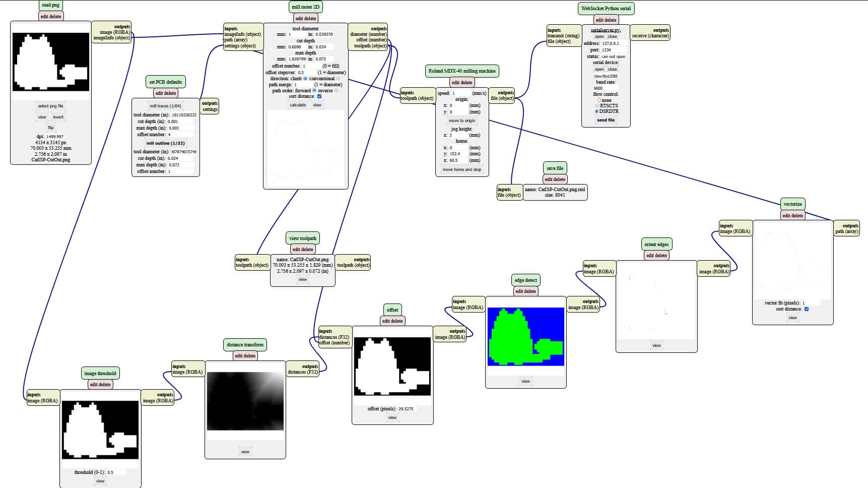
Creating the Toolpath with MODS
With the now finished Board design I exported it from KiCAD via
File > Export > SVG... to an SVG file. This file however could not be used like that
and first had to be changed in order to be used with Mods.
For this I loaded the svg file into GIMP, exported it as a PNG with low compression and subsequently
changed this png file. I got rid of the alpha channel by filling everything that wasnt coloured with
white. While Mods comes with a function to invert the colors of the svg, I simply used GIMPs own
functionality to create my finsihed traces png, which can be downlaoded in the download section.
In a similar fashion I created the outline for the PCB by filling everything in with black and
filling hte outside with white, and later on inverting the colors. This png can also be downloaded
in the downlaod section.
With the PNGs now ready to use with Mods, I loaded it up and used
Rightclick > programs > open server program > machines > Roland > mill > MDX-20 > PCB png.
This loaded up the program to create Toolpaths from my png files.
As I already wrote as part of the
group assignment, our milling machine at the lab in Kamp Lintfort is the Roland MDX-40. This meant
that I needed to change a few parameters in order to be able to create toolpaths for this machine.
The parameters that needed to change were part of the Roland MDX-20 milling machine
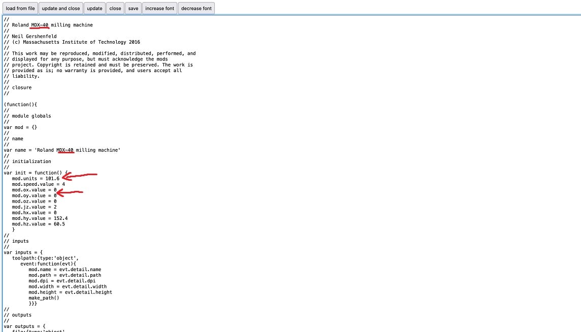
Node. I clicked on edit within the node and changed the mod.units variable in the
initialization from 40 to 101.6. This value was given to us by Ahmed who calculated it beforehand.
He also told us to change the origin values for the X/Y origin from 10/10 to 0/0. I then also
changed the name of the node to resemble our milling machine. The changed Code for this can be seen
here:
On top of theese changes other values were changed depending on wether the traces or the outline was
being calculated. For the traces I changed the Tool diameter in the set PCB defaults
and mill raster 2D Nodes to 0.23mm /This value was recommended by Ahmed for the tool we
would use as it was V-Shaped 0.2mm to 0.5mm) or roughly 0.009in. I then set the cut depth and the
max depth to 0.001 respectively and kept the other values the same. I finally added a
save file Node via Rightclick > Modules > open server module > file > save
and connected its input to the output of the changed milling machine node.
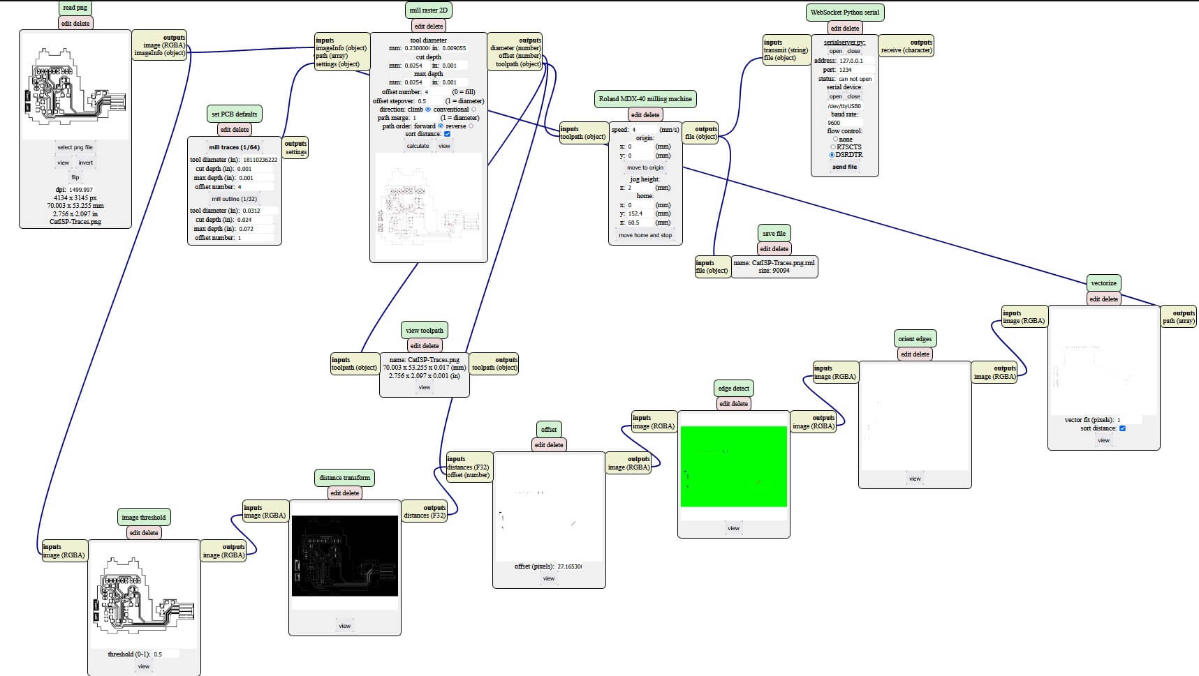
For the outline I changed the MDX-20 node the same way as described above but used different values
for the tool itself. I toggled the set PCB default Node to
mill outline(1/32) and set the tool diameter to 1mm or roughly 0.0394in. I left the
other values standard and just changed the speed of the milling node from 4mm/s to 1mm/s. The gcode
for both the traces and the outline can be downloaded below.
Milling the PCB
After creating the toolpaths for our milling machine, I was off to the machine to start milling. Since I milled the test piece for the group assignemnt before, the process was now known to me. I changed to milling bit from the 1mm bit to the V-Shaped 0.2mm-0.5mm bit and with the help of Ahmed found a piece of copper board that was big enough for my PCB-design. I attached tape to the backside and stuck the plate on the far left and lower corner of the vacuumable layer. I then homed the mill with the programm that comes with the roland mill. The interface of this program can be seen here:
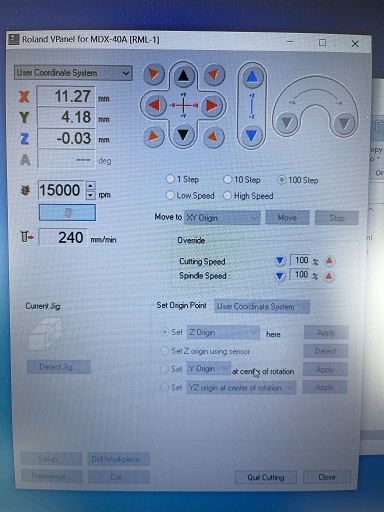
First on the X/Y axis to be as close to the corner of the copperplate as possible and after that the Z-axis. This was a little bit more tricky as I needed to have the drill running. While using very small steps I then tried to listen to the drill bit piercing the copper plate and so I began lifting the bit after a few small steps and looking onto the copper plate to see if there was a small scratch made by the drill bit. Since I dont quite know the difference between a small indent and a proper cut into the board, I asked Ahmed to take a look at the copperplate and decide wether the machine was homed good or bad on the z-axis.
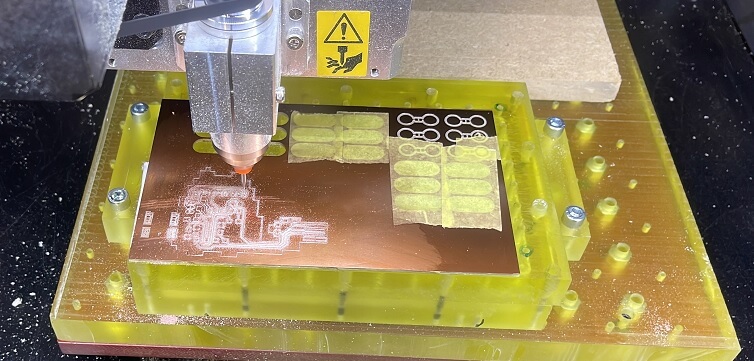
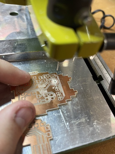
After homing, I loaded the toolpath into the program and began cutting. Since the milling amchine started with the names on the board, this was a good moment to stop the milling and take a look at the names. They were legible but Ahmed said it could be better. This was when I aborted the milling and homed the Z-Axis again. I also set the X/Y-origin to be more to the right to not cut the names twice at the same place. This time the cutting went more smoothly. While milling the copperplate looked like this:
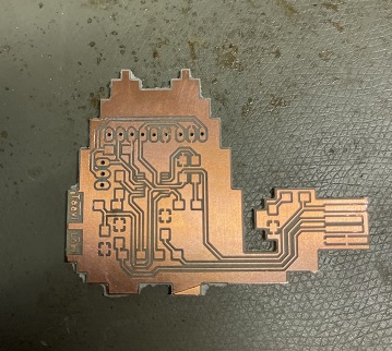
After the traces were cut, I changed the bit to a 1mm one and homed the Z-Axis again. This time with the help of the auto level sensor that is included with the machine. Since the bit has a larger diameter, the danger of breaking it while using the sensor is pretty small. With the Z-Axis homed again the PCB milling was finished. Sadly the copperplate was a little bit broken leading to one of the cats' feet to break. Ahmed quickly fixed this with superglue however. After the cutting was done, there were a few holes needed to be drilled. Instead of using the milling machine, Ahmed recommended to just use the proxon drill we have at the lab, since the number of holes to drill is pretty manageable.
After the holes were drilled this was the finished PCB without parts:
Stuffing the PCB
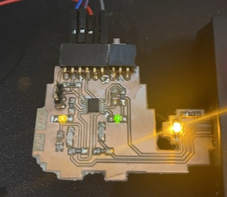
The same as milling, I never really have soldered before in my life and was quite afraid of this task as my hand steadiness is really terrible. I was more than surprised of the part sizes when I went through the BOM with Ahmed to search for all the needed parts in the lab. I was expecting small parts, but these sizes made me even more afraid of soldering. All needed components for the PCB can be found here. After I had all the parts together, Ahmed gave me a quick introduction to soldering again. After that I tried soldering my first component. Ahmed recommended to start of with the FTDI chip, which I did. I alligned the chip according to the schematic and soldered the first leg. Here I primariliy learned not to use too much solder as I overdid it extremely and had a massive blob of solder on the leg of the chip. With the wig i got it cleaned again though. After trying to solder the other legs next to the one I already had soldered I noticed that i used too much solder al the time, resulting in connections between the legs of the chip. To get rid of these connections I once again used the wig to scoop up the major part of solder mass and I was left with at least for me pretty good looking solder joints. These solderjoints are not perfect in any way, shape or form, but they work for the moment. Not all of the joints are shiny or have the perfect amount of solder on them, but some do and that made me very happy for soldering for the first time. I will do a better Job on my V2 of this board. After the chip I soldered the power LED and the associated resistor. After that I soldered the missing resistors for the FTDI chip and the pads for the USB-A port. Subsequently I tested the board by watching if the power LED would work, which it did. After that came the LEDs for Reading and Writing activity and after that came the Through-Hole Components with which I could later connect an arduino Ahmed gave to me to verify that the programmer was working. In comparison to the surface mounted compoenents the through hole components needed much more solder. Depending on where the legs were in comaprison to the others, the soldering was quite hard, as the tip of the soldering iron would not get perfectly in between the legs. It was also quite hard to get the solder to stick to every side of the legs as it sometimes kind of followed the soldering iron when I was removing it from theleg I was soldering. All in all I have to say that part of my fear of soldering was unwarranted. My not so steady hands however made alligning the small components on the pads not all to easy. I also had to learn that these small components are able to endure pretty high pressure when fixating them onto the pads. At first I was afraid of breaking the components when pressing to hard, but they are very durable. At the end I am quite satisfied with the endresult. There coulb be cleaner and better solderjoints but for my first time I was quite impressed that everything went as smooth as it did for me. No major hickups or other problems. So after the process of soldering all the components to the cut copper plate I had this PCB, which worked like expected when plugged into an USB-port:
Testing the PCB
To test if the programmer was working correctly, Ahmed gave me an Arduino uno which had a simple echo script running, where everything sent to the arduino would be returned. After connecting the Arduino to the corresponding pins on my board and inserting the board into the lab pc, I tested if the script would still work this way and to my surprise it really did! Here is a Video of the testing:
File Downloads
- KiCad-Project (Have to redo this, as the project was deleted from my drive by our printer in the lab :D)
- Traces PNG
- Toolpath traces for Roland MDX-40 (V-Shaped 0.2mm-0.5mm tool)
- Outline PNG
- Toolpath Outline for Roland MDX-40 (1mm tool)
- BOM