Individual Assignment Requirements
- Make and test a microcontroller development board that you designed.
- Document the complete process including PCB design, fabrication, assembly, and testing.
- Include original design files (schematic, PCB, toolpaths, and fabrication files).
- Demonstrate the functionality of the board.
- Include a hero shot of the final PCB.
Learning Outcomes
- Describe the process of toolpath generation for PCB fabrication.
- Understand PCB milling and laser engraving workflows.
- Apply soldering techniques for electronic assembly.
- Debug and test electronic circuits.
- Identify fabrication and design improvements.
Progress Status
Summary of PCB design, fabrication, and testing workflow.
Schematic and PCB layout designed in EasyEDA, including custom components and routing strategy.
DXF processed in Fusion 360 to generate G-code for milling, drilling, and cutting operations.
PCB milled using Makera Carvera CNC, including surface leveling and multi-step machining process.
Components soldered using flux and fine-tip soldering iron, including modular connectors for reuse.
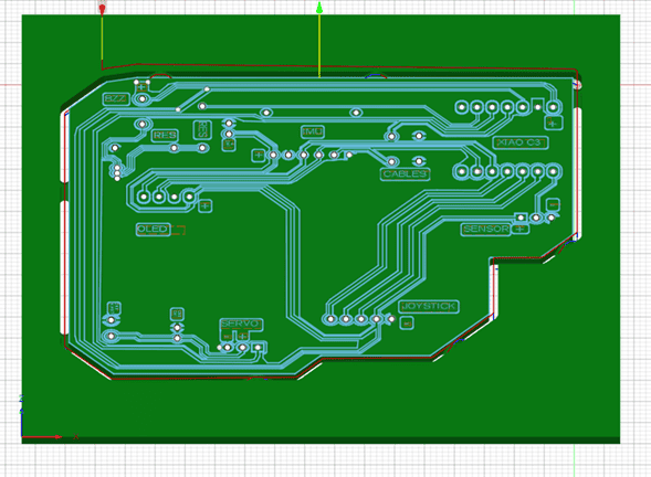
PCB Design – Schematic and Layout Development
For this assignment, I designed a custom PCB intended to integrate a XIAO ESP32C3 with multiple peripherals, including an OLED display, analog sensors, a joystick, a buzzer, a servo motor, and an IMU.
The main objective of this design was not only to create a functional circuit, but to develop a modular and reusable platform that could be used in future assignments such as input devices, output systems, and communication protocols.
This required careful planning of pin distribution, power management, and connector accessibility to ensure compatibility with different types of peripherals :contentReference[oaicite:0]{index=0}.
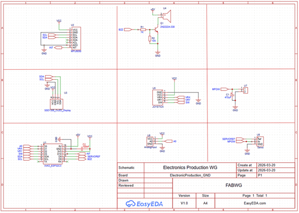
Schematic Design Strategy
The schematic was developed in EasyEDA, prioritizing clarity and logical organization. Instead of using long wires, I implemented net labels to simplify the diagram and reduce visual complexity.
This approach makes the circuit easier to understand and debug, especially when working with multiple interconnected modules such as sensors, displays, and communication interfaces.
Additionally, custom components were created in a local library to ensure that footprints matched real hardware dimensions, reducing the risk of misalignment during fabrication.
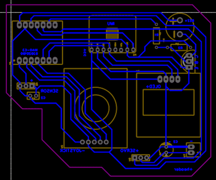
Component Placement and Routing
Once the schematic was validated, the design was transferred to the PCB editor. At this stage, component placement became a critical step, as it directly affects routing complexity and board usability.
The layout strategy considered:
- Logical grouping of components based on functionality
- Minimizing crossing traces and avoiding unnecessary vias
- Ensuring physical accessibility for connectors and modules
- Reducing overall board size without compromising usability
Routing was designed manually to maintain control over signal paths. A track width of 0.5 mm was selected to ensure reliable current flow, while a minimum clearance of 0.3 mm was defined to match the limitations of the CNC milling process :contentReference[oaicite:1]{index=1}.
These values were chosen as a balance between electrical performance and manufacturability, ensuring that traces would not be damaged during milling.
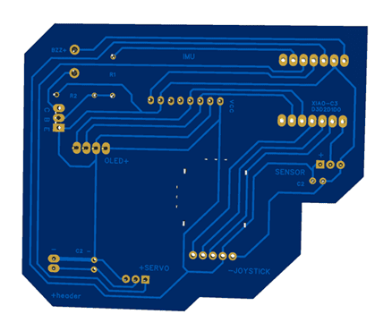
3D Verification and Design Validation
A 3D visualization of the PCB was generated to validate the physical arrangement of components before fabrication.
This step is especially important because it allows detecting issues that are not evident in 2D views, such as:
- Mechanical interference between components
- Incorrect orientation of connectors
- Insufficient spacing for cables or modules
By validating the design in 3D, potential fabrication errors can be avoided, reducing iteration time and material waste.
Board Definition and Export
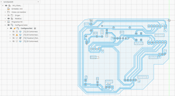
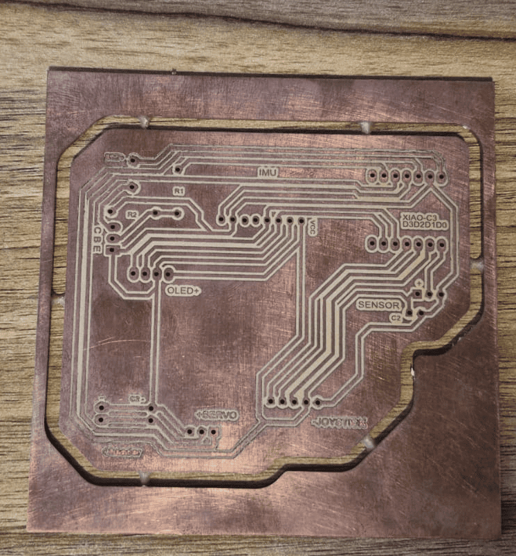
Instead of using a standard rectangular shape, the PCB outline was defined using a custom polyline geometry, optimizing the use of material and adapting the shape to the distribution of components.
Finally, the design was exported as Gerber files, which contain all the necessary information for fabrication, including traces, drill holes, and board outline. These files were later used in the CAM process to generate the toolpaths for CNC milling.
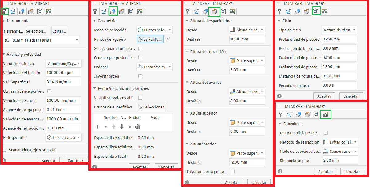
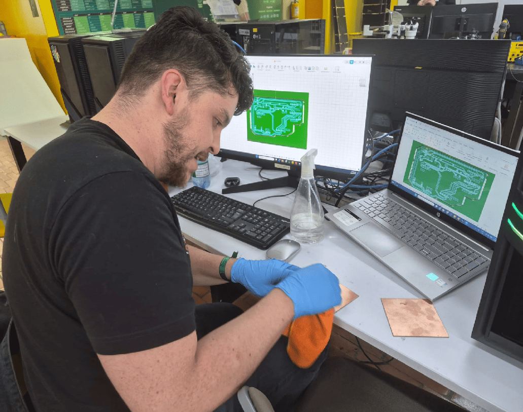
CAM Process – Toolpath Generation and CNC Preparation
After completing the PCB design, the next step was to prepare the board for fabrication using a CNC milling process.
The design files were exported as Gerber files and then converted into a DXF format, which contains the vector geometry required for toolpath generation.
These vectors were imported into Fusion 360, where the manufacturing workflow was defined and the G-code for the CNC machine was generated :contentReference[oaicite:0]{index=0}.
Machine Configuration
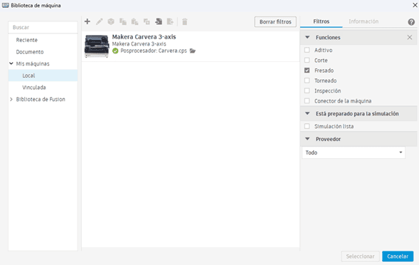
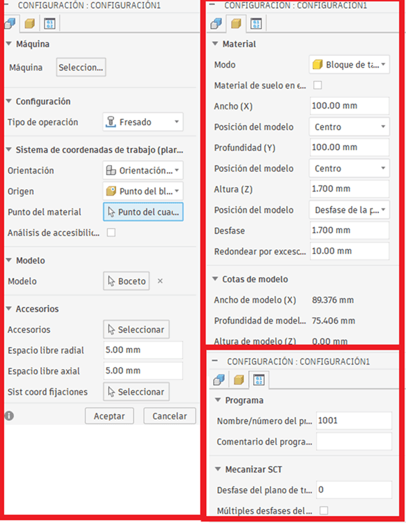
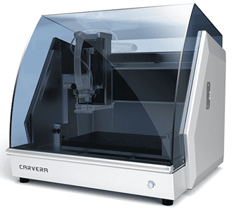
In Fusion 360, a manufacturing setup was created by selecting the Makera Carvera 4-axis CNC as the target machine.
The work area was defined according to the physical dimensions of the material (100 × 100 mm PCB), and the coordinate system was aligned with the stock origin.
This step ensures that the virtual model and the physical machine share the same reference system, which is critical for accurate fabrication.
Machining Strategy
The PCB fabrication process was divided into three main operations:
- Surface clearing (pocketing): removal of excess copper
- Drilling: creation of holes for through-hole components
- 2D contouring: cutting the board outline
This multi-step approach ensures electrical isolation, structural accuracy, and proper component integration.
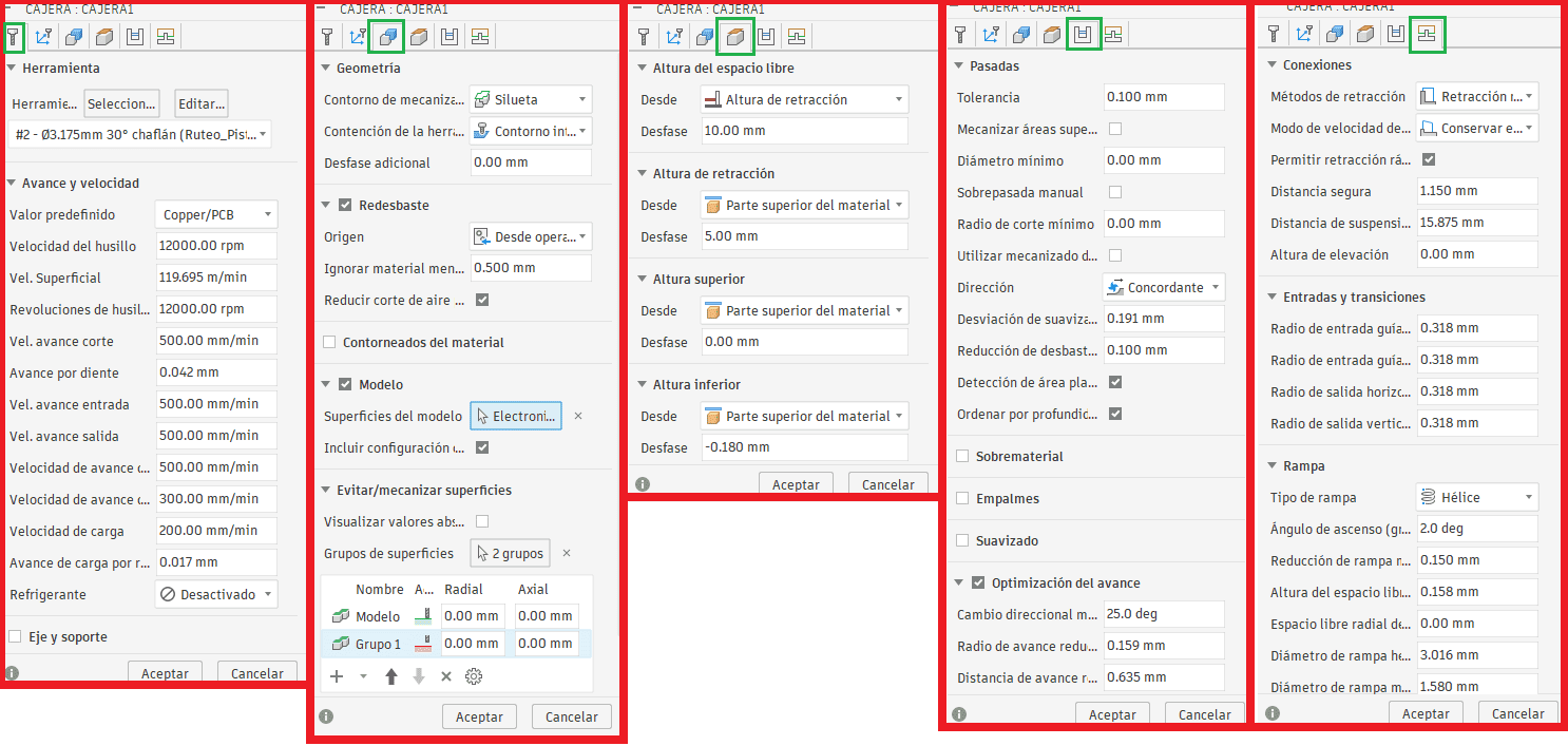
Surface Clearing (Copper Removal)
The first operation was a pocketing process, used to remove the excess copper around the traces.
A fine engraving tool (needle-type bit) was used to achieve high precision and avoid damaging narrow traces.
This step is critical to prevent short circuits by isolating conductive paths on the PCB surface.
Drilling Operation
The second operation consisted of drilling all required holes using a 1 mm drill bit, matching the component footprint design.
Accurate drilling ensures proper alignment of components and improves the reliability of solder joints.
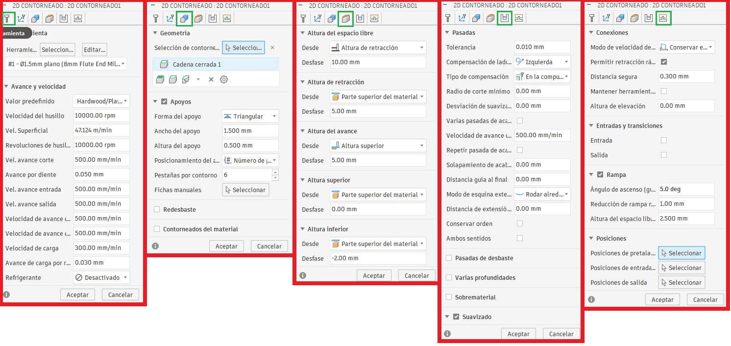
Board Cutting (2D Contour)
The final operation was a 2D contour cut, used to define the external shape of the PCB.
A larger milling tool (≈2.45 mm) was used to efficiently remove material and cut the board outline.
Small holding tabs were left to prevent the board from moving during machining.
Toolpath Simulation
Before exporting the G-code, a simulation was performed to verify toolpaths, detect potential collisions, and validate machining sequences.
This step is essential to avoid machining errors and ensure that the fabrication process runs smoothly.
G-Code Generation
After validating all operations, the toolpaths were post-processed into G-code, which was then transferred to the Carvera Controller software for execution on the CNC machine.
PCB Fabrication – CNC Milling Process
After generating the G-code, the fabrication process was carried out using the Makera Carvera CNC machine, working with a copper-clad board (bakelite) of 100 × 100 mm and 1.7 mm thickness.
The process required careful preparation of both the material and the machine to ensure precision and avoid defects during milling :contentReference[oaicite:0]{index=0}.
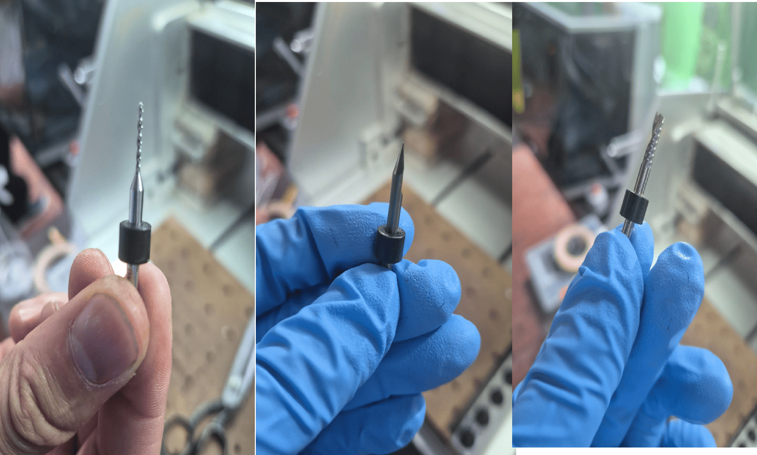
Tool Selection
Different tools were used depending on each machining operation:
- Fine engraving bit: for trace isolation
- 1 mm drill bit: for holes
- 2.45 mm end mill: for contour cutting
Selecting the correct tool for each operation was critical to balance precision, efficiency, and surface quality.
Material Preparation
Before machining, the copper surface was cleaned using isopropyl alcohol to remove dust, grease, and oxidation.
This step improves tool contact and ensures clean cuts, especially when working with fine traces.
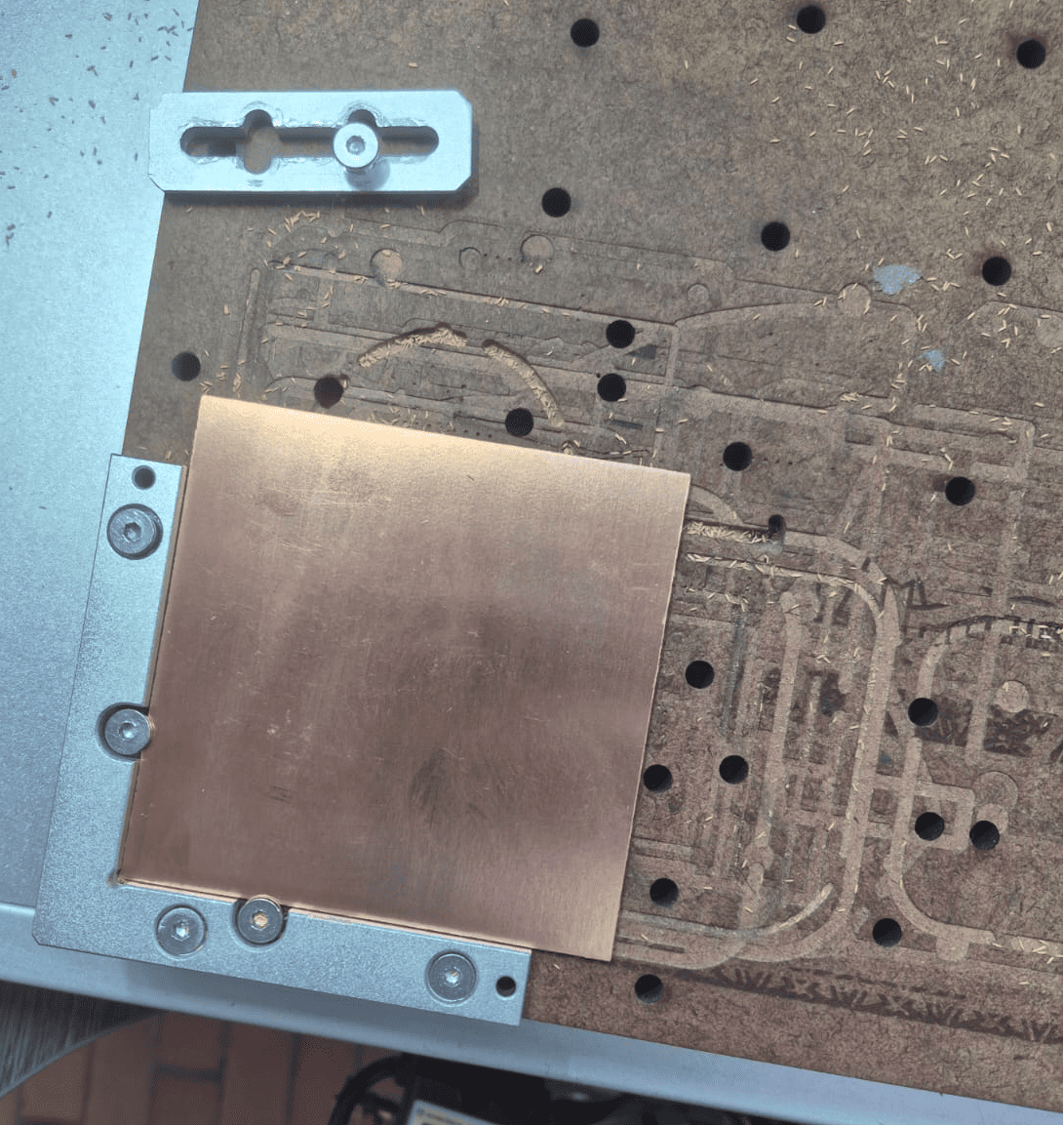
Workpiece Fixation
The PCB was mounted and secured using the machine clamps to prevent any movement during machining.
Proper fixation is essential, as even small displacements can cause misalignment, broken traces, or tool damage.
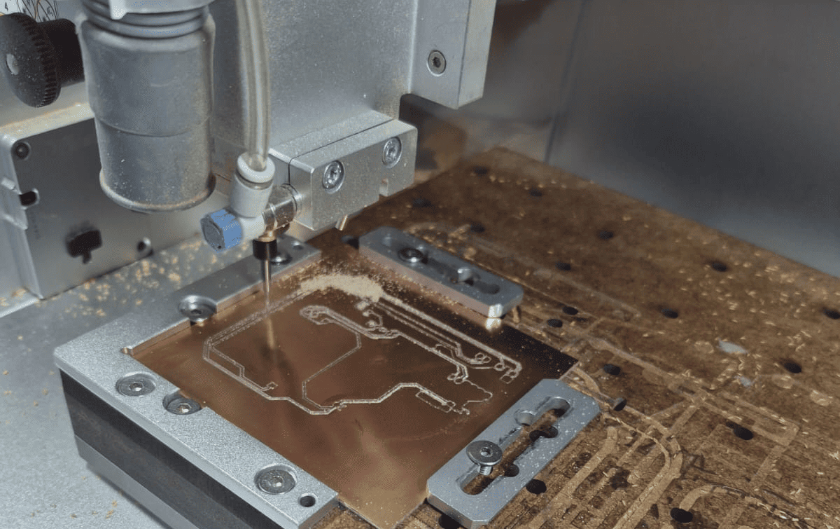
Milling Process
Once the setup was complete, the CNC machine executed the G-code, starting with an automatic surface probing routine to compensate for material irregularities.
The machining process included:
- Surface leveling and Z calibration
- Copper removal (trace isolation)
- Drilling operations
- Final contour cutting
The entire process took approximately 3 hours and 40 minutes.
CNC Milling Process
The following video shows the PCB fabrication process using the CNC machine, including trace milling and board cutting.
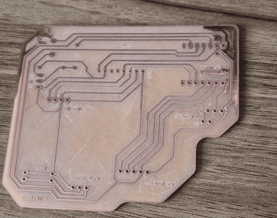
Final PCB Result
After machining, the PCB was removed from the stock by cutting the holding tabs and cleaned again to remove debris.
The final result showed well-defined traces and correct geometry, confirming that the toolpath generation and machining parameters were properly configured.
Electronics Assembly – Soldering and System Integration
After completing the PCB fabrication, the next step was assembling the electronic components and transforming the board into a functional system.
This stage required careful handling of components, precise soldering techniques, and validation of electrical connections to ensure correct operation :contentReference[oaicite:0]{index=0}.
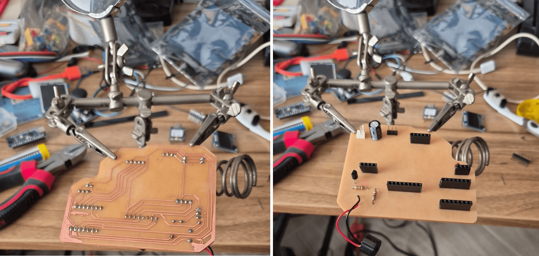
Soldering Process
The components were soldered using 60/40 tin-lead solder (1 mm diameter) and a 25W fine-tip soldering iron, allowing precise control over small pads and traces.
To improve solder quality, flux was applied to the pads before soldering. This helps remove oxidation, improves heat transfer, and ensures a strong electrical connection between the component and the copper surface.
Special attention was given to avoid cold joints, solder bridges, and overheating of components, which could compromise circuit reliability.
Modular Design Strategy
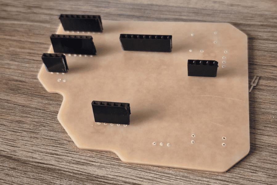
Instead of soldering all components permanently, female pin headers were used for external modules such as sensors and displays.
This design decision allows:
- Easy replacement of components
- Reuse of modules in future projects
- Flexible system configuration
This approach improves maintainability and extends the usability of the PCB beyond a single application.
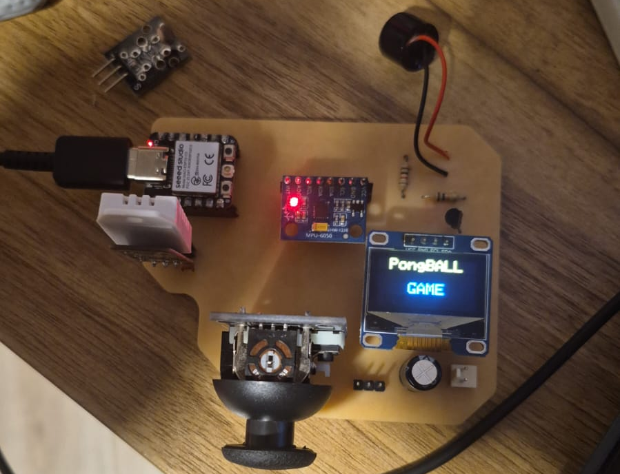
Testing and Validation
After assembly, the board was visually inspected to verify solder joints and ensure there were no short circuits or disconnected traces.
Electrical testing was then performed by powering the board and validating connections between the microcontroller and the peripherals.
This step confirms that the entire workflow—from design to fabrication and assembly—was successful.
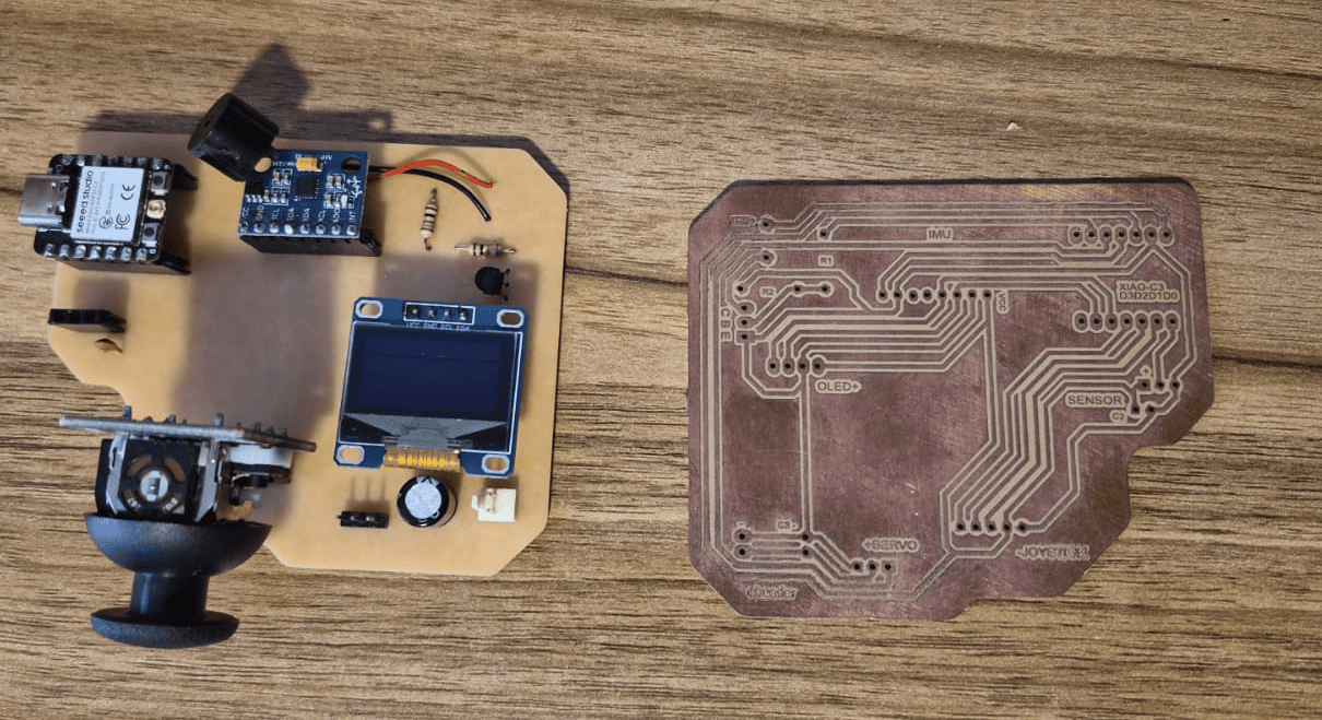
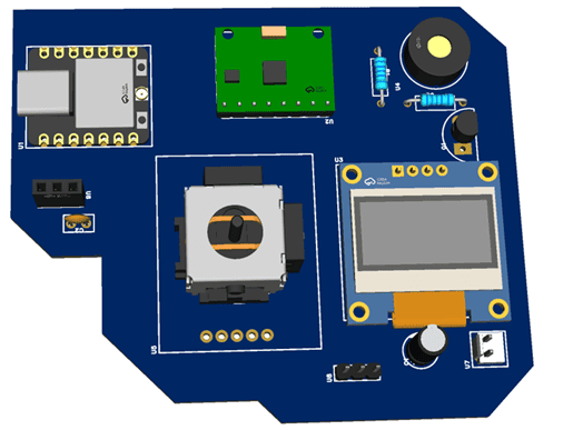
Final Result – Hero Shot
The final PCB integrates all required components into a compact and functional system, ready for use in future assignments.
This result demonstrates the complete electronics production workflow, from digital design to physical implementation.
Challenges and Errors – PCB Fabrication Issues
During the initial design iteration, a GND copper pour (ground plane) was added to the PCB in order to improve electrical performance by providing a common reference and helping with noise reduction.
However, this decision introduced unexpected challenges during the CNC milling process, particularly in the generation of toolpaths for copper removal.
Problem Description
During the milling process, some of the PCB traces were unintentionally removed or damaged.
This occurred because the toolpath offset was generated incorrectly, causing the milling tool to remove material from the inner side of the trace instead of the external boundary.
As a result, the effective width of certain traces was reduced or completely eliminated, breaking electrical continuity in the circuit.
Technical Analysis
This issue is directly related to how toolpath generation and offsets are defined in CAM software.
When working with a ground plane, the geometry becomes more complex because the software must decide which regions to remove and which to preserve. If the offset direction is not correctly defined, the milling tool can:
- Cut inside the trace boundary instead of outside
- Remove critical conductive paths
- Reduce trace width below manufacturable limits
This demonstrates that PCB milling is highly sensitive to tool diameter, offset direction, and geometry interpretation.
Solution and Design Adjustment
To solve this issue, the ground plane was removed in the next iteration of the design, simplifying the geometry and ensuring better control over the milling process.
Additionally, more attention was given to toolpath preview and simulation in Fusion 360, verifying that the milling operations correctly preserved all traces before generating the final G-code.
Lessons Learned
- Ground planes can introduce complexity in CNC PCB fabrication workflows.
- Toolpath direction and offset must always be validated before machining.
- Simulation is essential to detect potential errors before fabrication.
- Simpler designs are often more reliable for subtractive PCB manufacturing.
This experience reinforced the importance of understanding not only the design, but also how manufacturing processes interpret geometry.
Extra Credit – PCB Fabrication Using Laser Engraving
As an additional experiment, the same PCB design was fabricated using a laser engraving process, exploring an alternative method to traditional CNC milling.
This approach aimed to evaluate differences in precision, workflow, and manufacturing limitations between subtractive machining and laser-based fabrication.
Hybrid Fabrication Workflow
The fabrication process combined both CNC and laser technologies:
- First, drilling and contour cutting were performed using the CNC machine
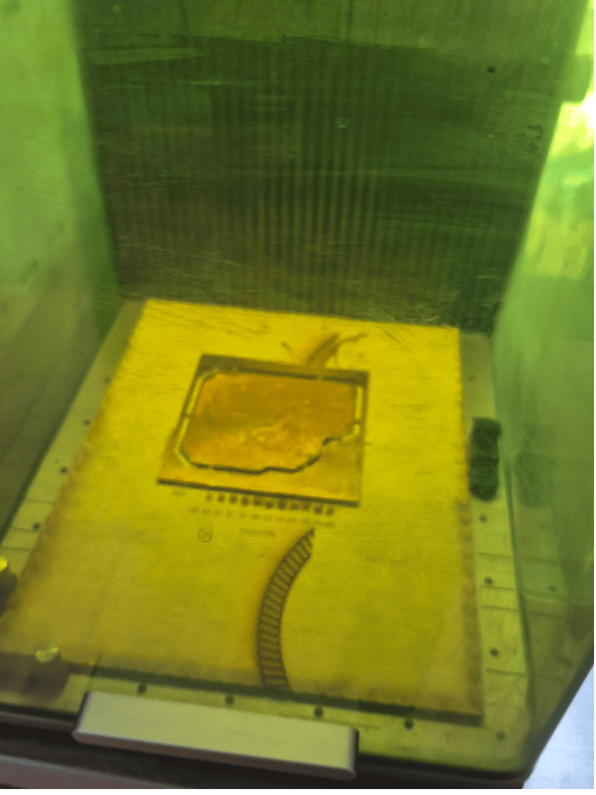
- Then, the PCB was transferred to the Xtool laser cutter
- A black-and-white image (DXF-based) was used to define engraving areas
In this process, the laser removes copper from the black regions, leaving the conductive traces intact.
Alignment and Positioning
One of the key advantages of the laser system is the use of an integrated camera, which allows precise positioning of the workpiece.
This feature made it possible to align the PCB with high accuracy, ensuring that the engraving process matched the previously machined geometry without misalignment.
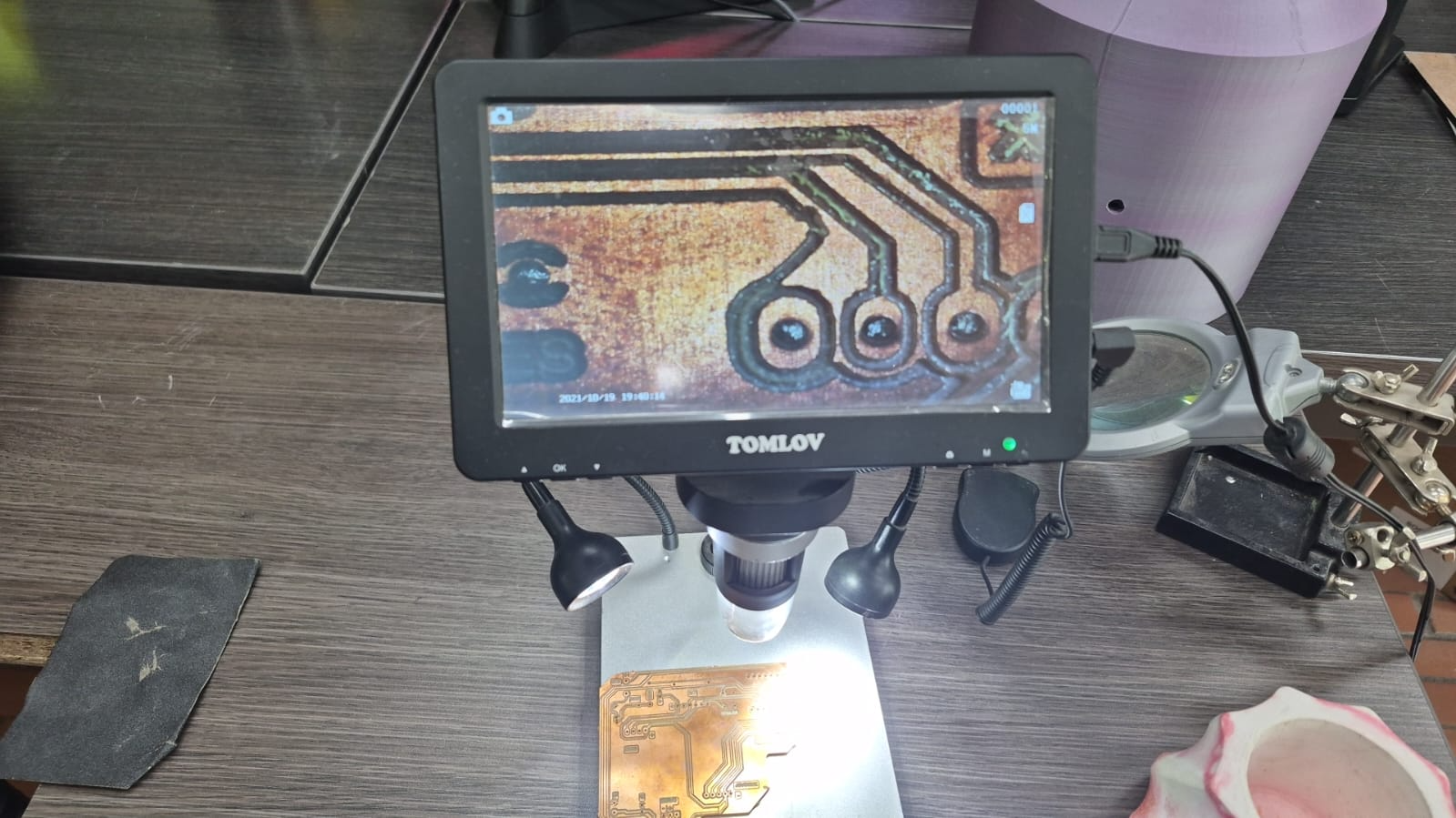
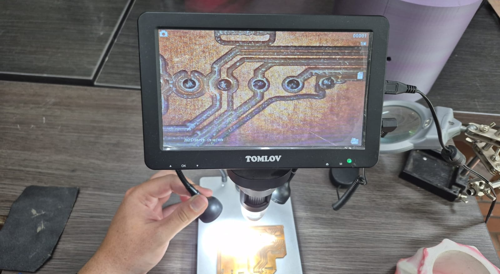
Engraving Process
The engraving process took approximately 12 hours, mainly due to the low laser power setting (30%) used to avoid damaging the copper layer or the substrate.
Although this significantly increased fabrication time, it ensured a controlled material removal process and preserved the integrity of fine traces.
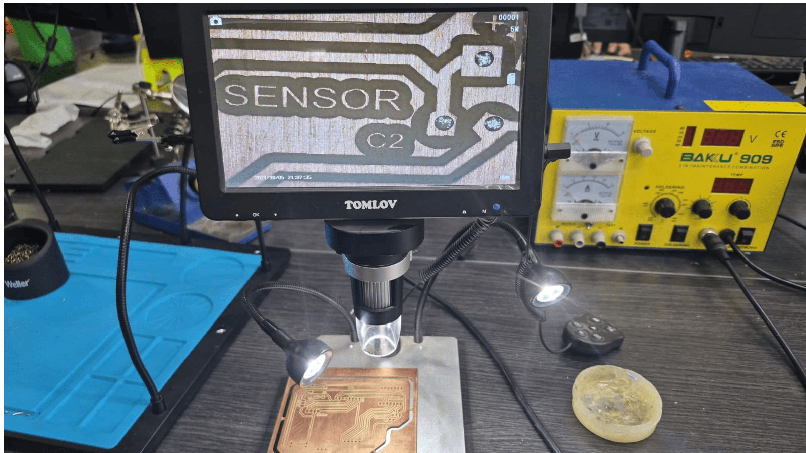
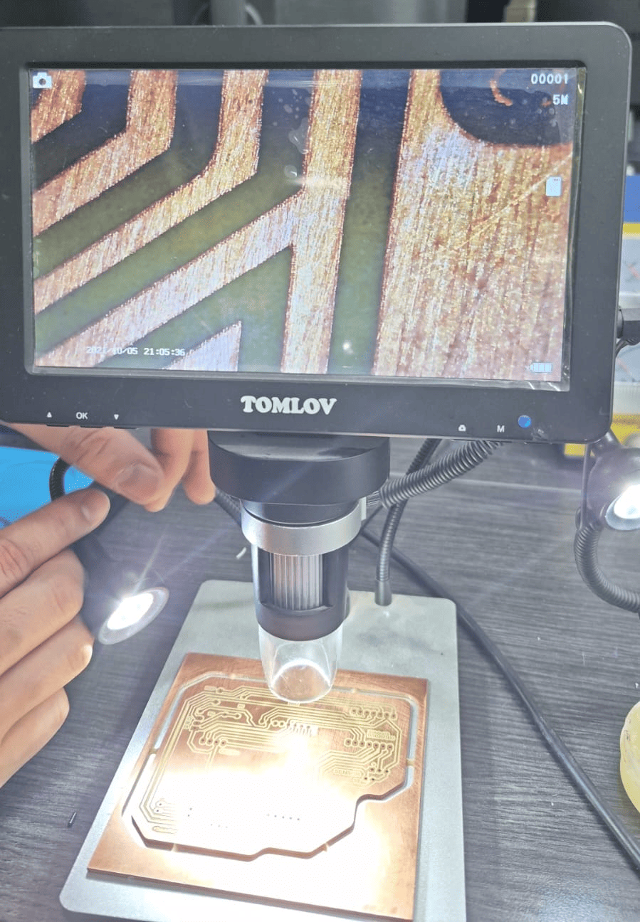
Microscopic inspection of PCB traces showing high precision and edge definition.
Laser Engraving Process
The following video shows the PCB engraving process using the laser cutter, highlighting the material removal strategy and precision of the method.
Comparison with CNC Milling
- Higher precision: laser engraving produced finer details compared to CNC routing.
- Better edge definition: traces showed cleaner boundaries under microscopic inspection.
- Longer fabrication time: significantly slower than CNC milling.
- Limited capabilities: laser cannot drill holes or cut the PCB.
This experiment demonstrated that while laser engraving offers superior precision, CNC machining remains more versatile for complete PCB fabrication workflows.
Final Reflection
This week provided a complete understanding of the electronics production workflow, from digital design to physical implementation. Unlike previous assignments, the focus was not only on functionality, but on how design decisions directly impact manufacturability.
One of the most important insights was realizing that PCB design is inherently linked to fabrication constraints. Parameters such as trace width, spacing, and component placement must be defined not only based on electrical requirements, but also considering the limitations of the manufacturing process.
The CAM process in Fusion 360 reinforced the importance of understanding how geometry is interpreted by machines. Toolpath generation is not just a technical step, but a critical translation between design and fabrication. Small mistakes in offsets or machining strategy can result in significant failures, such as the loss of traces observed during the initial iteration.
The fabrication phase highlighted the importance of machine setup and process control. Factors such as material fixation, surface cleaning, and tool selection directly affect the quality and reliability of the final PCB. The use of automatic surface probing in the CNC machine also demonstrated how modern tools compensate for material imperfections.
The assembly stage emphasized the role of precision and technique in soldering. The use of flux, appropriate tools, and careful handling of components ensured reliable electrical connections. Additionally, the decision to use modular connectors improved the flexibility and reusability of the board.
The errors encountered during the process were particularly valuable. The issue with the ground plane and incorrect toolpath offsets demonstrated how fabrication processes can misinterpret geometry, reinforcing the importance of simulation and validation before machining. These challenges transformed the workflow into an iterative process rather than a linear one.
The extra experiment with laser engraving provided an alternative perspective on PCB fabrication. While the laser method achieved higher precision and better edge definition, it also revealed limitations such as long processing times and the inability to perform drilling or cutting operations. This comparison highlighted that each fabrication method has trade-offs, and selecting the appropriate one depends on the design requirements.
Overall, this week strengthened my understanding of how to design for manufacturing, how to interpret and control fabrication processes, and how to evaluate different production methods. It also reinforced the importance of debugging, iteration, and critical analysis when working with real-world digital fabrication systems.
Individual Reflection (Group Assignment)
Participating in this group assignment gave me a much deeper understanding of the complete PCB manufacturing process. Rather than focusing only on designing a circuit, I learned that every stage—from defining design rules and generating toolpaths to milling, assembly, and debugging—has a direct impact on the quality and reliability of the final board.
One of the most valuable lessons was understanding how to adapt PCB designs to the capabilities of the available manufacturing equipment. Establishing appropriate trace widths, clearances, and machining parameters helped me design boards that could be fabricated consistently using the Makera Carvera CNC, reducing fabrication errors during subsequent assignments.
I also found it valuable to compare in-house CNC milling with commercial PCB manufacturing. While local fabrication is ideal for rapid prototyping and iterative testing, learning the integrated EasyEDA and JLCPCB workflow showed me how the same design can be prepared for professional manufacturing when higher precision or larger production volumes are required.
The knowledge gained during this group assignment became the foundation for my individual electronics assignments throughout Fab Academy. Having a standardized manufacturing workflow allowed me to focus on improving my circuit designs while confidently producing, assembling, and programming custom PCBs for the following weeks.
Downloads & Resources
This section provides access to the design resources and downloadable files created during the Electronics Production assignment. The repository includes the complete PCB fabrication workflow, from electronic design to CNC milling, laser engraving, soldering, and final board assembly.
🛠️ Project Resources
The project repository contains all files required to reproduce the electronic board, including editable PCB designs, machining files, and manufacturing documentation.
- ✅ EasyEDA Pro PCB Project
- ✅ PCB Layout (DXF)
- ✅ CNC Milling Toolpaths (G-code)
- ✅ Laser Engraving Files
- ✅ PCB Assembly Documentation
- ✅ Manufacturing Resources
📁 Downloadable Files
To improve the loading performance of this documentation website, all project files have been moved to a shared Google Drive folder.
The repository contains the EasyEDA project, PCB layout, CNC machining files, laser engraving resources, and supporting documentation created during the Electronics Production assignment.
Additional fabrication resources, board revisions, and updated documentation may be added as the project evolves.