Individual Assignment Requirements
- Use an EDA tool (KiCad / Eagle / etc.) to design a development board.
- Use components available in the Fab Lab inventory.
- Design a board capable of interacting and communicating with an embedded microcontroller.
- Ensure the board is manufacturable (design rules, trace width, clearances).
- Export production files (Gerbers and drill files).
Learning Outcomes
- Select and use software for PCB design.
- Understand schematic capture and PCB layout workflow.
- Apply design rules for fabrication.
- Route traces considering electrical and manufacturing constraints.
- Prepare files for PCB production.
Progress Status – Electronics Design
Summary of completed tasks for Week 06.
Created custom schematic symbols for specific components not available in the default EDA library.
Designed and verified custom PCB footprints, ensuring correct pad dimensions and spacing according to datasheet specifications.
Designed schematic centered on the XIAO ESP32-C3, integrating OLED (I2C), joystick (analog inputs), and buzzer (digital output).
Routed traces following Fab Lab milling design rules (trace width and clearance verified).
Performed Electrical Rules Check and Design Rules Check. No critical errors remaining.
Exported Gerbers, drill files and board outline ready for PCB production.
1. Component Creation – Custom Library Development
Project Reference – Wokwi System Diagram
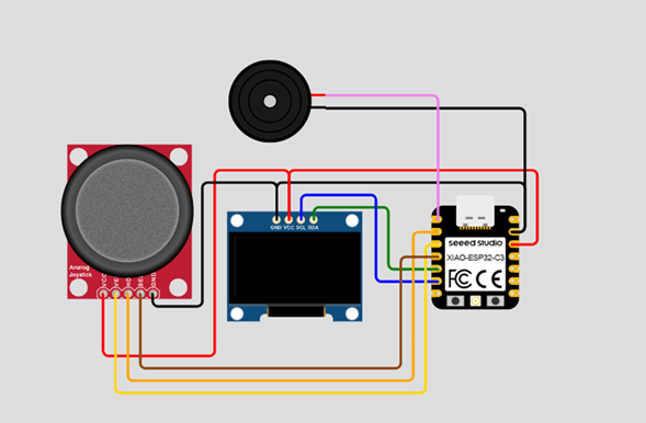
The PCB design was based on the embedded system developed in Week 04. The original Pong Game implementation included the XIAO ESP32-C3, an SSD1306 OLED display, an analog joystick, and a buzzer.
This simulation diagram served as the architectural reference for defining the hardware connections and signal mapping before starting the EDA workflow.
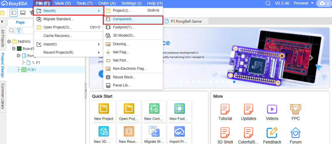
Creating a New Component in EasyEDA
The first step in the electronics workflow was creating custom components inside EasyEDA.
Using the “Create Component” tool, I generated a new schematic symbol for the XIAO ESP32-C3 module, instead of relying on default libraries.
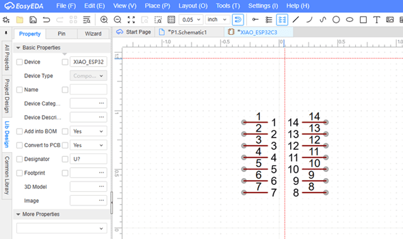
Pin Distribution Definition
The XIAO ESP32-C3 has 14 pins arranged in two rows. Using a digital caliper, I measured the physical dimensions:
- Pin spacing: 0.1 in
- Distance between rows: 0.6 in
- Board width: 0.72 in
- Board height: 0.84 in
Each pin was manually created and renamed to match the official microcontroller pinout.
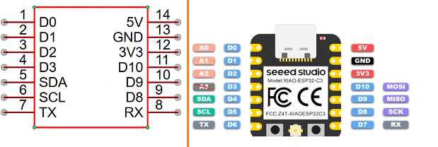
Verification Against Official Datasheet
After defining the schematic symbol, I compared it with the official XIAO ESP32-C3 pinout diagram from the datasheet.
This verification step ensured correct signal naming, voltage labeling (5V, 3V3, GND), and communication pins such as SDA, SCL, RX, and TX.
Cross-checking with the official documentation prevents critical routing errors later in PCB layout.
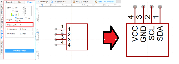
Using the Wizard Tool for Faster Component Creation
For simpler components such as the OLED display, I used the EasyEDA Wizard tool.
By specifying the number of pins and orientation, the software automatically generated the schematic symbol, which was later customized with correct pin names: VCC, GND, SDA, and SCL.
This method speeds up development while maintaining precision and clarity in schematic documentation.
2. Footprint Design – Physical Layout Definition
Pin Distribution and Pad Configuration
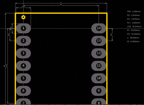
After completing the schematic symbols, the next step was designing the PCB footprints. The XIAO ESP32-C3 footprint was created using the official pin distribution provided in the datasheet and the Seeed Studio reference page:
https://wiki.seeedstudio.com/PCB_Design_XIAO/
All pad spacing and distances were verified using a digital caliper to ensure real-world dimensional accuracy.
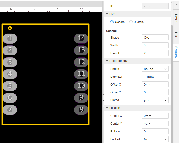

Dimension Verification
The “Check Dimension” tool in EasyEDA was used to verify spacing between pads and overall footprint dimensions.
This step ensures mechanical compatibility before PCB fabrication, preventing alignment issues during soldering.
Verifying dimensions at this stage significantly reduces fabrication errors and rework.
3D Model Integration
After completing the footprint, a 3D model from the EasyEDA library was assigned to the component.
The 3D model was not custom-modeled; instead, an existing official model was used to ensure realistic visualization and mechanical validation.
This allows verification of height, clearance, and overall board proportions.
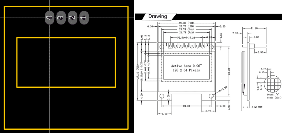
SSD1306 Footprint Validation
The same footprint creation process was repeated for the SSD1306 OLED display.
The footprint was compared against its mechanical dimensional drawing to ensure accurate hole placement and mounting alignment.
Cross-checking schematic, footprint, and mechanical drawing ensures full hardware consistency.
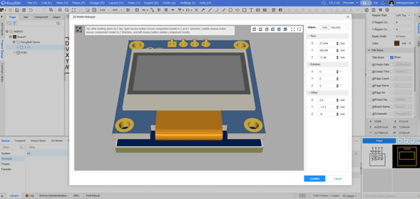
3D Model Positioning Tool
EasyEDA provides a dedicated tool to correctly position the 3D model relative to the footprint.
This tool is essential for adjusting translation and rotation, ensuring that the virtual 3D representation aligns perfectly with the pad layout.
Proper 3D alignment allows accurate visualization of component placement and helps identify potential mechanical interferences before manufacturing.
3. Schematic Design – System Integration and Verification
Component Placement in Schematic Sheet
After creating the custom components and footprints, the next step was placing all elements inside the schematic sheet.
The XIAO ESP32-C3 was positioned as the central controller, with the OLED display, joystick, and buzzer arranged logically around it according to their functional relationship.
Proper spatial organization improves readability and reduces confusion during later PCB routing stages.
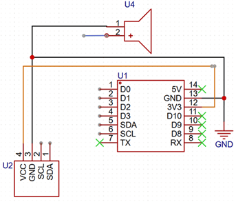
Power Connections and Unused Pins
The first connections established were power (VCC) and ground (GND) for all modules.
Ensuring common ground reference is critical for stable operation, especially when mixing analog (joystick) and digital (I2C, buzzer) signals.
Unused pins were explicitly marked using the “No Connect” (X) symbol, which prevents floating nets and eliminates warnings during rule checking.
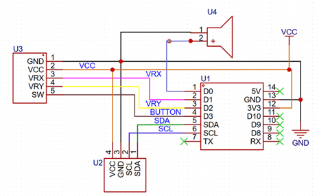
Signal Labeling and Visual Organization
Each signal was labeled according to its function: SDA, SCL, VRX, VRY, BUTTON, VCC, and GND.
Different colors were applied to improve visual clarity and follow schematic readability best practices.
Proper net labeling avoids unnecessary long wires, keeps the schematic clean, and simplifies debugging.
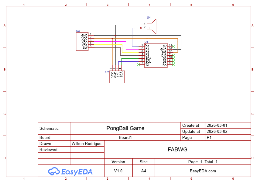
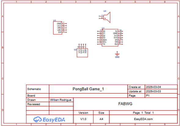
Completed Schematic
Once all connections were defined, the schematic was reviewed to verify logical consistency between modules.
The joystick analog outputs were connected to ADC-capable pins, the OLED display to I2C lines, and the buzzer to a GPIO configured for digital output.
At this stage, the system architecture was fully defined before transitioning to PCB layout.
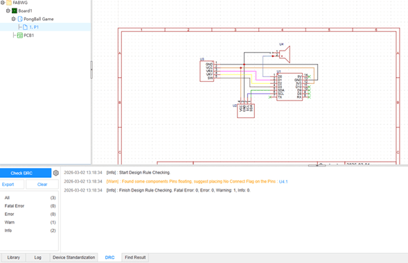
Design Rule Check (DRC) and Error Debugging
The final step was running the Design Rule Check (DRC) tool to detect electrical inconsistencies.
During this process, one of the buzzer connections was incorrectly assigned, generating a warning.
After correcting the net connection, the schematic passed the DRC with no critical errors, confirming electrical integrity before PCB export.
4. PCB Layout – Physical Implementation
Importing Components from Schematic
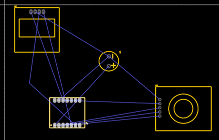
Once the schematic passed the DRC verification, the design was exported to the PCB workspace.
By applying the “Update PCB from Schematic” function, all components and their associated footprints were automatically imported into the board editor.
At this stage, the components appear connected by airwires, indicating logical connections that must be physically routed.
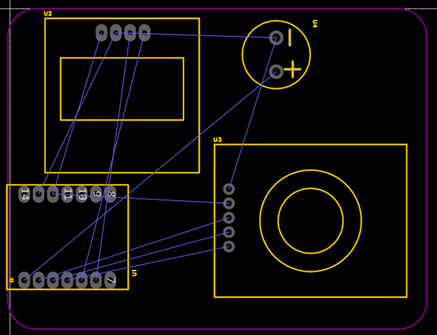
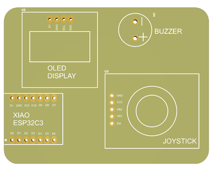
Component Placement and Board Outline
Components were arranged strategically to minimize crossing traces and maintain logical grouping.
The board outline was drawn using the Board Outline layer, defining the physical dimensions of the PCB.
Rounded corners were applied to improve aesthetics and mechanical finish.
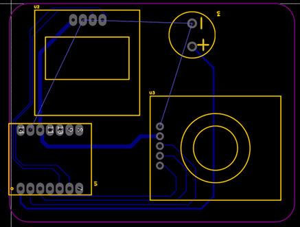
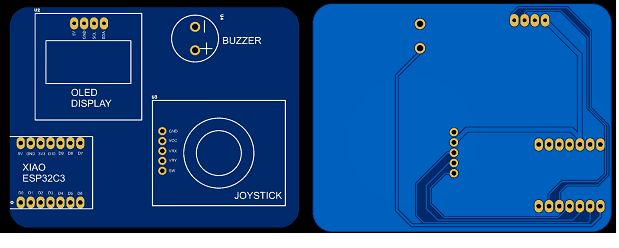
Trace Routing
Connections were routed manually using the trace tool on the bottom layer.
Power lines were prioritized first, followed by signal traces (I2C, analog inputs, and buzzer output).
Ground traces were intentionally left unrouted to later apply a full ground copper pour.
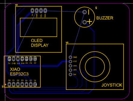
Silkscreen Labels and Pin Identification
Text labels were added to the silkscreen layer to identify each component and pin header.
Clear labeling improves usability, debugging, and future maintenance of the board.
Device names such as OLED DISPLAY, JOYSTICK, BUZZER, and XIAO ESP32C3 were added to enhance visual clarity.
Ground Plane (GND Copper Pour)
A copper pour connected to GND was applied on the bottom layer to create a continuous ground plane.
This improves electrical stability, reduces noise in analog signals, and simplifies routing by eliminating the need for multiple ground traces.
The ground mask was carefully checked to ensure all ground pads were properly connected.
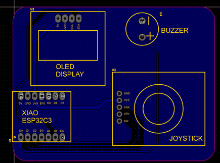
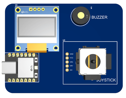
5. 3D Model Visualization – Mechanical Validation
EasyEDA provides an integrated 3D visualization tool that allows real-time rendering of the PCB after footprints and components are fully defined.
This tool is essential for mechanical validation, enabling verification of:
- Component height and spatial distribution
- Relative positioning accuracy
- Clearances between modules
- Board proportions and mechanical consistency
The 3D viewer allows inspection from multiple angles, helping detect possible mechanical conflicts before fabrication.
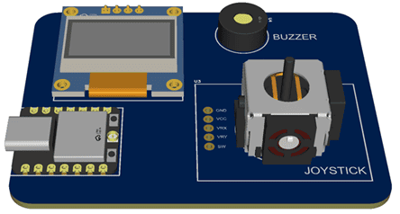
Complete 3D Model View
Component Distribution
Top View – No Solder Mask
Top and Bottom View
6. Fabrication Files – Production Ready Outputs
After completing the PCB layout and verifying all design rules, the final step was generating the fabrication files required for manufacturing.
Using the EasyEDA fabrication export tool, Gerber files and drill files were generated, including:
- Top and Bottom Copper Layers
- Solder Mask Layers
- Silkscreen Layers
- Board Outline
- NC Drill File
All files were reviewed using the integrated Gerber viewer to ensure correct layer generation and alignment.
The complete fabrication package is available in the Downloads section of this page, including the original EasyEDA design files and Gerber outputs.
At this stage, the board is fully prepared for PCB production and assembly.
Final Reflection – Electronics Design
This week significantly deepened my understanding of the complete PCB design workflow, from conceptual system architecture to production-ready fabrication files.
One of the most valuable lessons was understanding the relationship between schematic symbols, footprints, and real physical components. Creating custom components from scratch forced me to carefully analyze datasheets and verify mechanical dimensions using precision measurement tools.
The footprint design stage highlighted how small dimensional inaccuracies can translate into major assembly issues. Verifying pad spacing, alignment, and 3D model positioning reinforced the importance of mechanical validation before fabrication.
During schematic development, applying proper net labeling, marking unused pins, and running DRC checks helped me understand professional design practices and debugging workflows. Identifying and correcting a connection error before exporting the PCB strengthened my confidence in the verification process.
The PCB layout phase was particularly insightful. Strategic component placement, manual routing, and implementing a ground plane improved my awareness of signal integrity and electrical stability.
Overall, this assignment transformed my perception of electronics design from simply connecting modules to engineering a manufacturable and mechanically validated system. I now better understand how design decisions directly impact fabrication quality, reliability, and usability.
Individual Reflection – Group Assignment
This assignment was particularly valuable in reinforcing the importance of understanding embedded systems at the signal level. Beyond simply programming a microcontroller, it is essential to analyze how signals behave physically and how devices communicate.
The multimeter test helped revisit fundamental electrical concepts such as voltage, current, and resistance, while also highlighting the difference between DC measurements and the interpretation of PWM signals as average voltage values.
The logic analyzer provided a deeper level of insight, allowing precise visualization of PWM signals and accurate measurement of parameters such as period and pulse width using cursors. This made it possible to clearly understand how duty cycle affects system behavior.
The most advanced part of the assignment was the analysis of I2C communication, where it was possible to observe real data exchange between the microcontroller and the OLED display. This demonstrated how abstract communication protocols are implemented at the hardware level.
From an educational perspective, this assignment is highly relevant, as it bridges theoretical concepts with real-world measurements. It highlights the importance of teaching embedded systems not only from a programming standpoint, but also from a hardware and signal analysis perspective.
Overall, this experience strengthened my understanding of embedded systems and provided valuable insights that can be directly applied in teaching mechatronics and electronics courses.
Downloads & Resources
This section provides access to the design resources and downloadable files created during the Electronics Production assignment. The project includes PCB design files, manufacturing outputs, and fabrication documentation required to reproduce the electronic board.
🛠️ Project Resources
The resources developed during this assignment include the complete PCB design, fabrication files, and editable project files used for manufacturing and future hardware revisions.
- ✅ EasyEDA Pro PCB Project
- ✅ Gerber Manufacturing Files
- ✅ PCB Production Documentation
- ✅ Manufacturing Outputs
- ✅ Editable Design Files
📁 Downloadable Files
To improve the loading performance of this documentation website, all project files have been moved to a shared Google Drive folder.
The repository contains the complete EasyEDA Pro project, Gerber fabrication package, manufacturing documentation, and supporting files created during the Electronics Production assignment.
The EasyEDA project can be imported directly using File → Open Project → Import Local Project.