Group Assignment
- Characterize the design rules for the in-house PCB production process.
- Document the machine settings used for PCB fabrication.
- Document the workflow for sending a PCB to a board house.
- Publish the documentation on the group page and reflect on the individual page.
Learning Outcomes
- Describe the complete PCB fabrication workflow.
- Demonstrate tool-path generation, milling, stuffing, debugging and programming.
- Identify opportunities to improve the manufacturing process.
Machine & Workflow
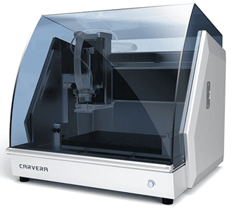
Makera Carvera CNC machine used for in-house PCB production.
PCB Production Equipment
The in-house PCB manufacturing process was carried out using a Makera Carvera CNC. This desktop CNC machine allows high-precision PCB fabrication by combining automatic tool changing, surface probing, drilling, engraving, and contour cutting in a single workflow.
For this characterization, FR-1 copper-clad boards were used together with dedicated engraving bits, drill bits, and end mills to perform trace isolation, drilling operations, and final board cutting.
- Machine: Makera Carvera CNC
- Material: FR-1 Copper Board
- Fabrication: Isolation Milling
- Automatic Z-Probing
- Automatic Tool Changing
Manufacturing Workflow
The PCB production workflow follows a repeatable sequence that ensures consistent fabrication results while minimizing machining errors.
Generate Toolpaths
Prepare Material
CNC Milling
PCB Inspection
Component Stuffing
Programming
Debugging
Functional Test
Characterizing this workflow allowed the group to establish a standardized PCB production process that can be consistently reproduced for future Fab Academy assignments.
Design Rules Characterization
Before designing and manufacturing PCBs, it is important to establish design rules that match the capabilities of the in-house CNC milling process. These rules define the minimum trace width, spacing, clearances, and other parameters that ensure reliable PCB fabrication without broken traces or electrical shorts.
For our Fab Lab, the design rules were configured in EasyEDA according to the manufacturing capabilities of the Makera Carvera CNC. These parameters were then used as the reference for all PCB designs developed during Fab Academy.
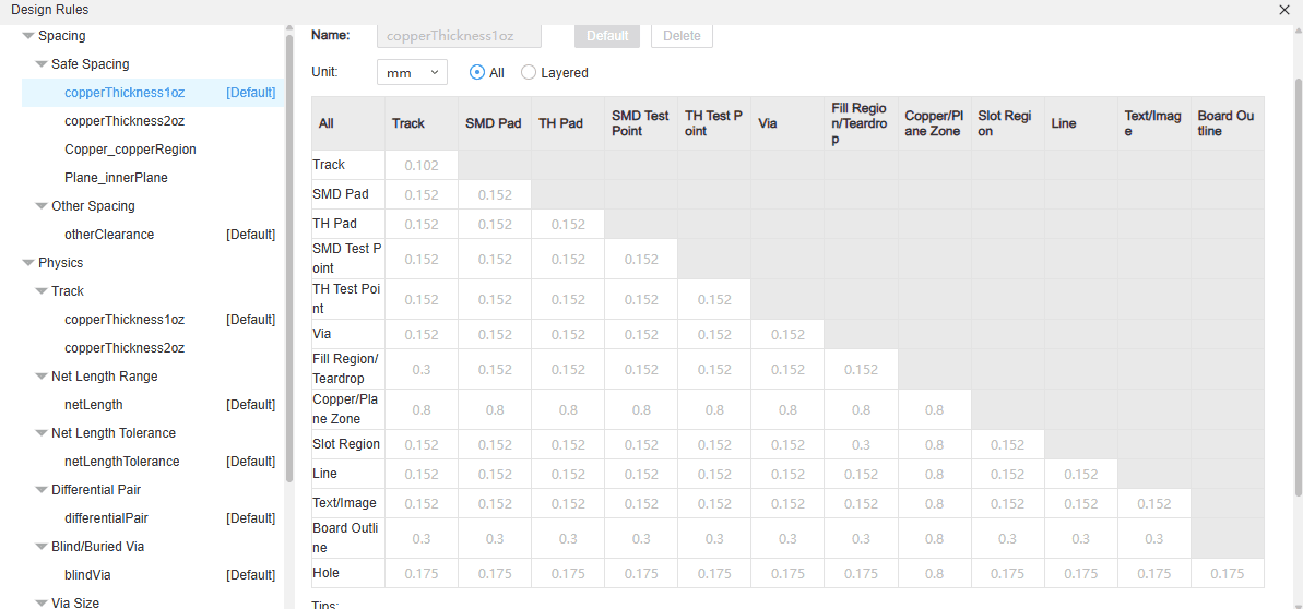
Track width configuration used during PCB design.
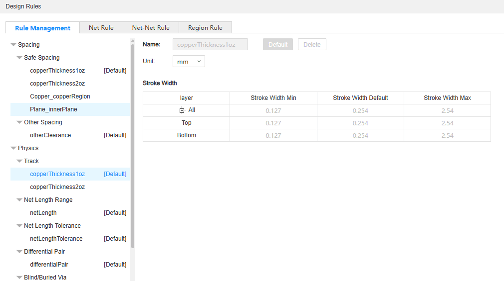
Clearance and spacing rules configured in EasyEDA.
Design Parameters
| Parameter | Value |
|---|---|
| Minimum Track Width | 0.127 mm (5 mil) |
| Default Track Width | 0.254 mm (10 mil) |
| Maximum Track Width | 2.54 mm |
| Minimum Track Clearance | 0.102 mm (4 mil) |
| General Clearance | 0.152 mm (6 mil) |
| Board Outline Clearance | 0.300 mm |
| Hole Clearance | 0.175 mm |
Defining these design rules before starting the PCB layout helps ensure that traces, pads, and clearances remain compatible with the CNC milling process, reducing the probability of manufacturing errors and improving the overall reliability of the boards.
PCB Production Workflow
After defining the design rules and generating the toolpaths, the PCB fabrication followed a standardized workflow using the Makera Carvera CNC. The objective was to establish a repeatable manufacturing process that could be applied to future Fab Academy projects while ensuring consistent fabrication quality.
1. Machine Preparation
The PCB was manufactured using the Makera Carvera CNC. Before machining, the appropriate cutting tools were selected according to each manufacturing operation, including trace isolation, drilling, and board contour cutting.
- Fine engraving bit
- 1 mm drill bit
- 2.45 mm end mill
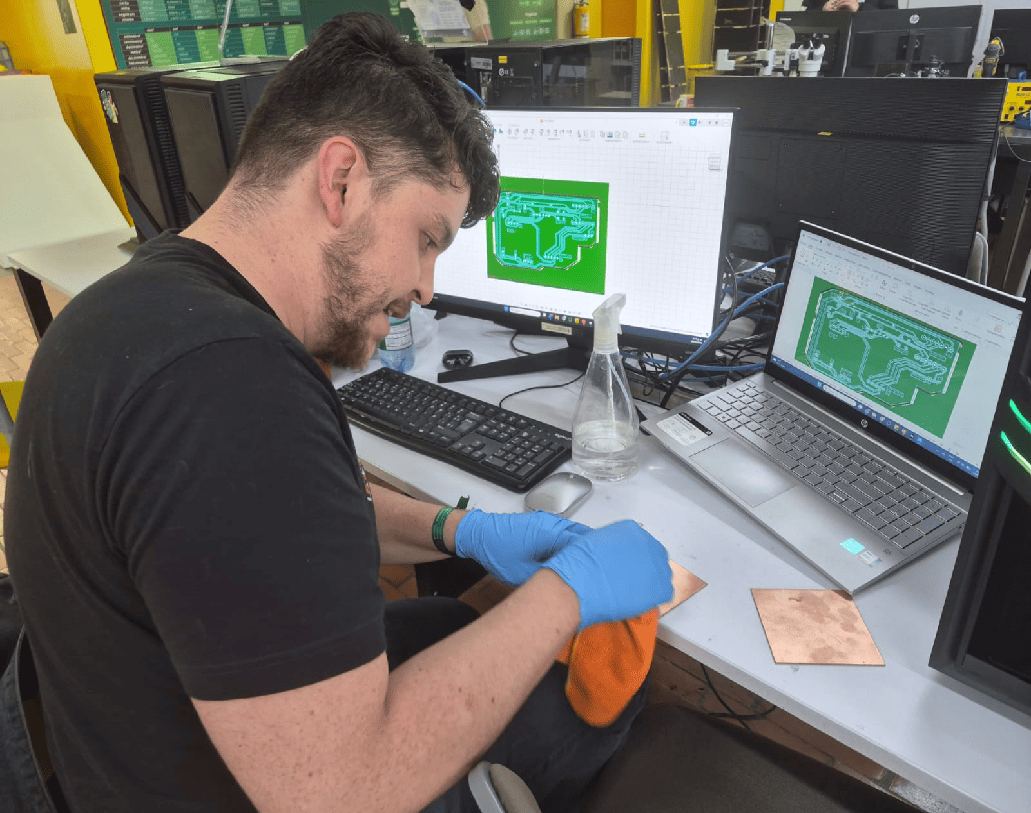
2. Material Preparation
The FR-1 copper board was cleaned using isopropyl alcohol to remove dust, grease, and oxidation. Afterwards, the workpiece was securely mounted inside the CNC machine to avoid movement during milling.
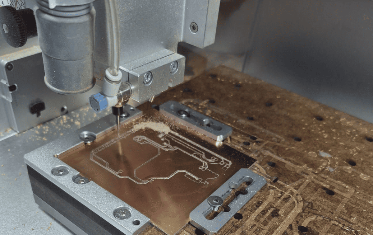
3. CNC Milling Process
The machining sequence began with automatic Z probing, followed by trace isolation, drilling operations, and contour cutting. This automated workflow minimized setup errors while ensuring accurate tool positioning and consistent milling quality.
PCB fabrication using the Makera Carvera CNC, including automatic probing, trace isolation, drilling, and contour cutting.
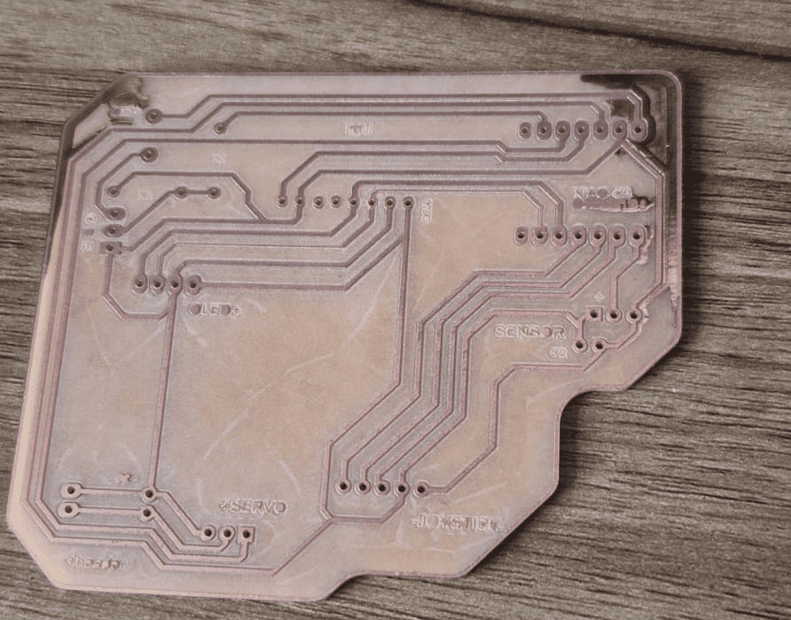
4. Final Inspection
Once machining was completed, the PCB was removed from the stock, cleaned, and visually inspected. The fabricated board presented clean trace isolation and accurate geometry, confirming that the selected design rules and machining parameters were appropriate for the in-house PCB production process.
Commercial Board House Workflow
Besides in-house PCB fabrication, EasyEDA provides an integrated workflow for manufacturing boards through JLCPCB. This feature simplifies the transition from PCB design to commercial production by automatically generating the required manufacturing files and transferring the project to the online quotation system.
Once the PCB design is completed and verified, the manufacturing process can be initiated directly from EasyEDA by exporting the Gerber files or selecting the "Order PCB/FPC at JLCPCB" option available in the export menu. This integration eliminates manual file preparation and reduces the possibility of configuration errors.
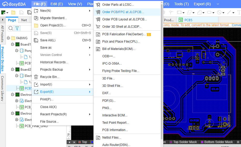
EasyEDA provides a direct export option to JLCPCB or allows downloading the complete Gerber package for any PCB manufacturer.
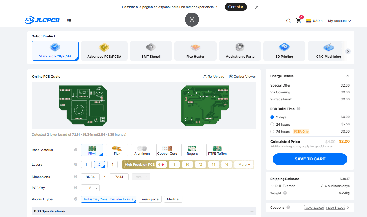
After uploading the Gerber files, JLCPCB automatically detects the board dimensions, layers, and manufacturing parameters for quotation.
Integrated Manufacturing Workflow
Design PCB
Run DRC
Export Gerbers
Upload to JLCPCB
Manufacturing
During the quotation process, the manufacturer automatically reads the Gerber files and identifies parameters such as board dimensions, number of layers, drill files, and copper geometry. Additional options including PCB thickness, surface finish, solder mask color, quantity, and shipping method can then be customized before confirming the order.
This integrated workflow significantly simplifies the transition from prototype development to professional manufacturing, making it possible to produce high-quality PCBs with minimal additional preparation.
In-house CNC vs Commercial Board House
During this group assignment, we compared both PCB manufacturing workflows. Each approach offers different advantages depending on the stage of the development process. In-house milling is ideal for rapid prototyping and iterative testing, while commercial board houses provide higher precision and professional manufacturing quality for final products.
| Feature | In-house CNC Milling | Commercial Board House |
|---|---|---|
| Turnaround Time | Same day | Several days + shipping |
| Ideal For | Rapid prototyping | Final production |
| Design Changes | Very easy | Requires a new order |
| Manufacturing Quality | Good for prototypes | Industrial quality |
| Number of Layers | Single / Double layer | Multilayer supported |
| Surface Finish | Raw milled copper | Professional finishes (HASL, ENIG, etc.) |
| Best Use Case | Fab Academy development and testing | Final products and production runs |
Understanding both manufacturing workflows allows designers to select the most appropriate fabrication method according to the project requirements. Throughout Fab Academy, in-house CNC milling enables fast iteration and immediate validation, while commercial board houses provide a reliable path toward manufacturing production-ready PCBs.
In-house CNC vs Commercial Board House
During this group assignment, we compared both PCB manufacturing workflows. Each approach offers different advantages depending on the stage of the development process. In-house milling is ideal for rapid prototyping and iterative testing, while commercial board houses provide higher precision and professional manufacturing quality for final products.
| Feature | In-house CNC Milling | Commercial Board House |
|---|---|---|
| Turnaround Time | Same day | Several days + shipping |
| Ideal For | Rapid prototyping | Final production |
| Design Changes | Very easy | Requires a new order |
| Manufacturing Quality | Good for prototypes | Industrial quality |
| Number of Layers | Single / Double layer | Multilayer supported |
| Surface Finish | Raw milled copper | Professional finishes (HASL, ENIG, etc.) |
| Best Use Case | Fab Academy development and testing | Final products and production runs |
Understanding both manufacturing workflows allows designers to select the most appropriate fabrication method according to the project requirements. Throughout Fab Academy, in-house CNC milling enables fast iteration and immediate validation, while commercial board houses provide a reliable path toward manufacturing production-ready PCBs.
Downloads & Resources
This section provides access to the design resources and downloadable files created during the Electronics Production assignment. The repository includes the complete PCB fabrication workflow, from electronic design to CNC milling, laser engraving, soldering, and final board assembly.
🛠️ Project Resources
The project repository contains all files required to reproduce the electronic board, including editable PCB designs, machining files, and manufacturing documentation.
- ✅ EasyEDA Pro PCB Project
- ✅ PCB Layout (DXF)
- ✅ CNC Milling Toolpaths (G-code)
- ✅ Laser Engraving Files
- ✅ PCB Assembly Documentation
- ✅ Manufacturing Resources
📁 Downloadable Files
To improve the loading performance of this documentation website, all project files have been moved to a shared Google Drive folder.
The repository contains the EasyEDA project, PCB layout, CNC machining files, laser engraving resources, and supporting documentation created during the Electronics Production assignment.
Additional fabrication resources, board revisions, and updated documentation may be added as the project evolves.