System Integration Tasks
- Create a system integration plan
- Define subsystem interactions
- Document integration using CAD and sketches
- Plan mechanical and electronic assembly
Documentation Requirements
- Describe integration strategy
- Show CAD models and system layout
- Explain packaging approach
- Link documentation to the final project page
System Integration Status
By the end of the development process, all planned subsystems were successfully integrated into a single educational platform. The controller architecture, electronics, mechanical design and system integration strategy were validated and implemented as part of the final project.
Project objectives and educational approach fully defined.
Hardware, software and communication architecture completed.
All electronic components selected and validated.
Internal layout and enclosure design completed.
PCB architecture and subsystem connections completed.
All subsystems successfully integrated and documented.
System Integration Overview
🚀 Related Final Project
This assignment documents a specific stage of the development of the GameLab Controller. For complete documentation, fabrication files, programming details and final results, visit the Final Project page.
View Final Project DocumentationThe GameLab Controller was conceived as an educational embedded systems platform that combines user interaction, sensor acquisition, visual feedback, and external device control within a single handheld device. Rather than developing independent electronic modules, the project was designed from the beginning as a unified system where hardware, software and mechanical components work together to provide a complete learning experience.
The purpose of the System Integration stage was to define how all these subsystems would interact inside a compact enclosure before moving to fabrication and implementation. This included the organization of internal electronics, mechanical constraints, communication interfaces, power distribution, and expansion capabilities.
Final CAD render of the GameLab Controller showing the integrated educational embedded systems platform.
At the center of the system is an ESP32-S3 microcontroller, selected for its processing capabilities, integrated wireless connectivity and extensive GPIO resources. The ESP32-S3 acts as the main coordination unit, managing user inputs, sensor data, graphical output and communication with external peripherals.
The controller integrates several embedded subsystems including a TFT graphical display, joystick controls, push buttons, a 3-axis IMU for motion sensing, RGB status indication and dedicated expansion interfaces. These elements were intentionally selected to expose users to multiple embedded systems concepts while maintaining a compact and intuitive form factor.
Integrated Subsystems
- ESP32-S3 main processing unit
- TFT display user interface
- Analog joystick module
- Push button inputs
- 3-axis IMU motion sensor
- NeoPixel RGB status indicator
- USB-C communication and power
- Power management circuitry
Expansion-Oriented Design
Unlike traditional fixed-function controllers, the GameLab Controller was designed as an expandable development platform. Two dedicated GPIO expansion ports allow users to connect additional devices such as buzzers, relays, environmental sensors, actuators and custom modules without modifying the main PCB.
This approach transforms the controller into a portable experimentation platform capable of supporting future projects and educational activities. The expansion interfaces were considered from the earliest design stages, ensuring that mechanical, electrical and software integration could support both the built-in peripherals and future external modules.
The following sections describe how these subsystems were organized, connected and integrated through mechanical design, electronic design and assembly planning to create a cohesive embedded systems platform.
Integration Plan
The primary objective of the GameLab Controller was not simply to create a handheld device, but to develop an educational embedded systems laboratory capable of reducing the barriers commonly faced by beginners. Traditional learning approaches often require students to purchase multiple electronic components, understand wiring diagrams, build temporary circuits, and debug connection errors before they can even begin exploring embedded programming.
To address these challenges, the project was conceived as a portable platform where the most commonly used peripherals are already integrated into a single device. This allows students to focus on programming, sensor interaction, communication protocols, and system behavior rather than spending excessive time assembling hardware connections.
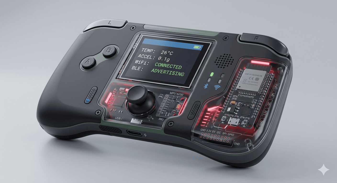
Initial integration concept showing the complete GameLab Controller platform.
Integration Strategy
The integration strategy focused on combining essential embedded systems peripherals into a single educational platform while preserving the flexibility required for experimentation and future expansion.
Instead of designing a fixed-function controller, the project was planned as a modular development platform centered around an ESP32-S3 microcontroller. The system integrates a graphical interface, motion sensing, user inputs, visual indicators and power management while providing expansion ports for additional devices.
This approach allows users to begin learning immediately using the integrated peripherals and later expand the platform with external sensors, actuators and custom modules as their knowledge grows.
System Architecture Planning
The ESP32-S3 was selected as the central processing unit due to its wireless connectivity, processing capabilities and large number of available GPIOs. All integrated peripherals were organized around the ESP32-S3 using communication interfaces commonly found in modern embedded systems.
Integrated Peripherals
- 1.8" RGB TFT Display (SPI)
- ADXL345 3-axis IMU (I2C)
- Analog joystick module
- Four multi-purpose push buttons
- Four status LEDs
- NeoPixel RGB indicator
Power & Communication
- ESP32-S3 microcontroller
- USB-C programming interface
- Li-Po battery (3.7V / 500mAh)
- HW-373 charging module
- Boost converter power stage
- Main power switch
Mechanical Integration Planning
The mechanical integration process began with the external shape of the controller rather than the electronics. The overall form factor was designed first to provide a familiar and ergonomic handheld experience inspired by modern gaming devices.
Once the external geometry was defined, the location of the display, joystick, buttons, LEDs and motion sensor was planned according to usability and accessibility requirements. This process ensured that all interaction elements remained comfortable to use while maintaining a compact internal structure.
After the internal arrangement was established, the electronic architecture was developed to support the selected component positions and simplify assembly inside the enclosure.
Electrical Integration Planning
During the electronics design stage, the initial objective was to integrate all subsystems into a single PCB. However, fabrication constraints imposed by the available PCB stock required an alternative solution.
To overcome this limitation, the system was divided into two interconnected boards. This approach preserved the original functionality while enabling fabrication using the available manufacturing resources.
Main PCB
- ESP32-S3 microcontroller
- TFT display interface
- ADXL345 IMU module
- Power management circuitry
- Boost converter
- Main power switch
- NeoPixel RGB LED
- Four status LEDs
Secondary PCB
- Four multi-purpose buttons
- GPIO Expansion Port 1
- GPIO Expansion Port 2
- Interconnection bus to main PCB
Expansion-Oriented Design
One of the main design goals was ensuring that the platform could evolve beyond its integrated peripherals. For this reason, two dedicated GPIO expansion ports were included in the architecture.
These ports provide direct access to ESP32-S3 resources, including ADC and touch-capable pins, allowing users to connect additional modules without modifying the main PCB. Examples include buzzers, relays, analog sensors, LEDs, servos and motor control systems using external drivers such as H-Bridge modules.
By combining integrated educational peripherals with expansion capabilities, the GameLab Controller becomes more than a handheld device. It functions as a portable embedded systems laboratory capable of supporting progressive learning experiences, experimentation and future development projects.
CAD & Mechanical Integration
The mechanical integration of the GameLab Controller was developed in SolidWorks. The objective was to design an enclosure capable of organizing and protecting all the electronic subsystems while keeping the device comfortable to hold and easy to understand as an educational platform.
Controller Form Factor Development
The design process started with the sketch of the external outline of the controller. Instead of starting directly from the PCB, I first defined the shape of the product based on ergonomic references from standard game controllers such as Xbox controllers and portable gaming devices.
These references helped define a familiar handheld shape, suitable for interaction with both hands. After defining the first outline, the controller was expanded symmetrically by approximately 20 mm. This extra space was necessary to include the TFT display and to provide enough internal area for the electronics.
The larger size was also influenced by fabrication limitations in the Fab Lab. Since the PCB had to be designed as a single-sided board, the electronic layout required more physical space for routing, jumpers and component placement.
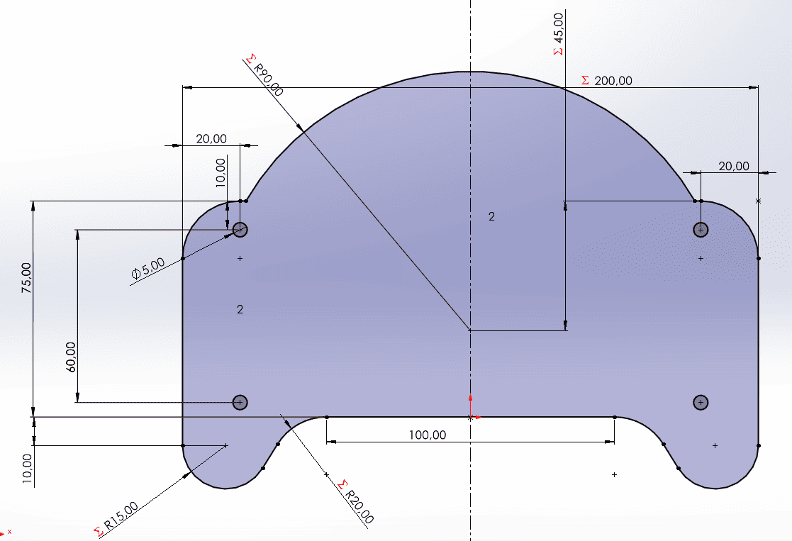
Initial controller outline developed in SolidWorks using commercial controllers as dimensional references.
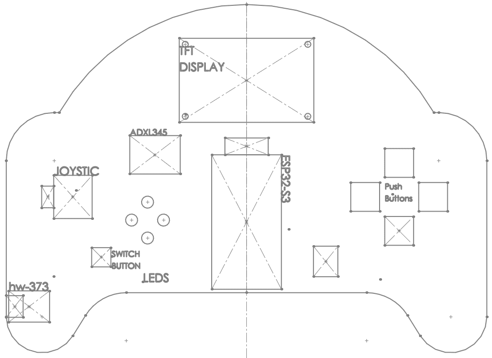
Internal layout planning for the display, joystick, buttons, LEDs, ESP32-S3 and IMU module.
Internal Layout Planning
Once the external contour was defined, the next step was to distribute the main components inside the controller. The TFT display was placed in the central area because it works as the main visual interface of the system.
The joystick, four multi-purpose buttons, LEDs, ESP32-S3 and ADXL345 IMU module were positioned around the display according to usability, visibility and assembly requirements. This helped define the relationship between the mechanical design and the electronic architecture.
Planning the component positions before completing the PCB was important because the mechanical design needed to support the user interface, the internal wiring, the removable ESP32-S3 and the separation between the main PCB and the secondary button PCB.
Two-Part Enclosure Design
The controller enclosure was divided into two main parts: the main housing and the top cover. The housing works as the container for the electronics and provides the internal volume needed for the PCB, joystick module, battery and interconnection cables.
A dedicated extra space was included for the 3.7V Li-Po battery. This was important because the battery should not collide with the PCB or apply pressure to the electronic components. Separating the battery space also helps with cable routing and future maintenance.
The top cover is thinner and contains the openings required for the visible and accessible components: the ESP32-S3, TFT display, four buttons, LEDs, GPIO expansion ports and main power switch.
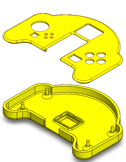
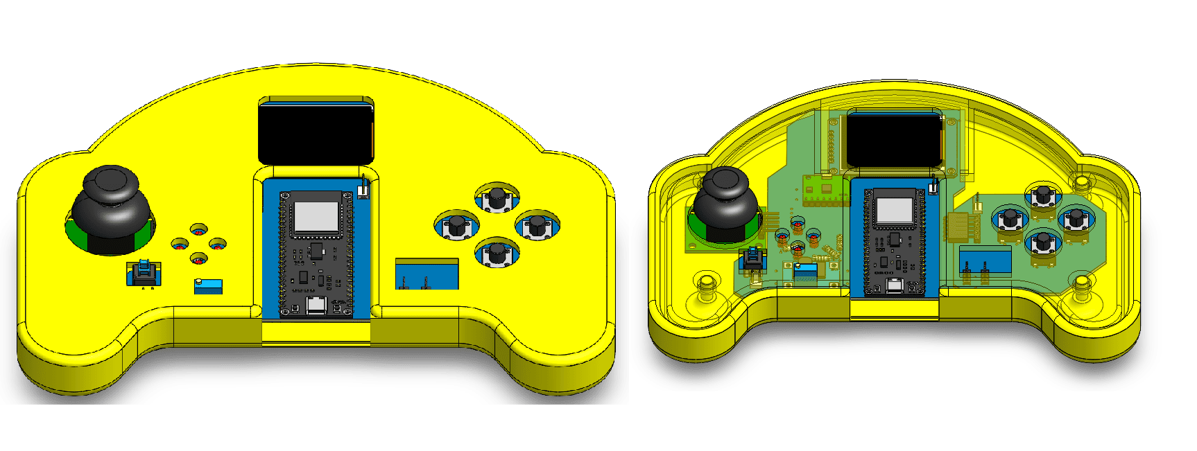
Main housing and top cover designed as two separate pieces for easier assembly and maintenance.
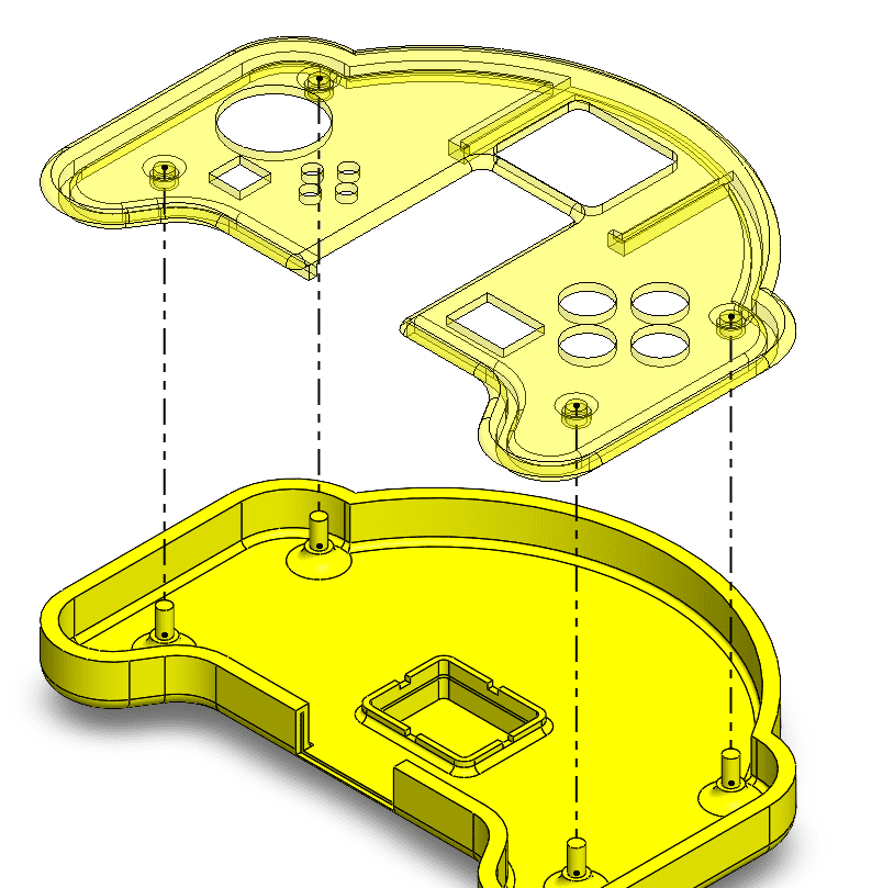
Cylindrical supports, female sockets and perimeter alignment lip used to improve the fit between both enclosure pieces.
Assembly and Alignment Features
To improve the mechanical assembly, four cylindrical supports were added inside the housing. These supports help align the top cover with the main body and provide contact points between both pieces.
The top cover includes matching female features where the cylindrical supports can fit. This creates a more controlled assembly and reduces unwanted movement between the two parts.
A 3 mm raised perimeter lip was also added to the cover. This feature works as an alignment guide, helping both pieces fit together more precisely and improving the final appearance of the enclosure.
These details are important for system integration because the enclosure is not only cosmetic; it defines how the electronics are positioned, protected and accessed.
Design for Maintenance and Reuse
A key mechanical decision was to keep the ESP32-S3 removable. Since the project is an educational laboratory, the microcontroller should not be treated as a permanently fixed component. Leaving enough clearance around the ESP32-S3 allows it to be removed and reused in other projects.
This decision affected the shape of the top cover, which includes a large opening around the ESP32-S3 area. The opening improves access for programming, debugging, replacement and reuse.
The final mechanical design therefore supports the educational purpose of the project: it packages the electronics into a finished-looking device, but still keeps the system accessible, understandable and modifiable.
By combining ergonomics, internal organization, battery clearance, removable electronics and alignment features, the CAD design became a central part of the system integration strategy.
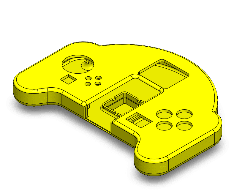
Final CAD model showing the mechanical integration strategy for the GameLab Controller.
Hardware Integration (Electrical Design)
The electrical design of the GameLab Controller was developed with the goal of integrating all the essential elements required for an embedded systems learning platform into a single device. The architecture combines sensing, user interaction, visual feedback, power management and expansion capabilities around an ESP32-S3 microcontroller.
During the system integration stage, special attention was given to the relationship between the electronic architecture and the mechanical design. Since all components had to fit inside a handheld enclosure, the schematic and PCB layouts were developed considering both functionality and available fabrication resources.
System Schematic
The schematic was designed around an ESP32-S3 development board acting as the central processing unit of the platform. All peripherals were connected through interfaces commonly used in embedded systems, providing students with exposure to multiple communication protocols.
The TFT display communicates through SPI, while the ADXL345 accelerometer uses the I²C bus. The joystick is connected through analog inputs, and the four push buttons are connected through digital GPIOs. Additional GPIO ports were included to support future expansion using external sensors and actuators.
The power subsystem includes a rechargeable 3.7V Li-Po battery, an HW-373 charging module, a power switch and a boost converter to provide stable voltage to the entire system.
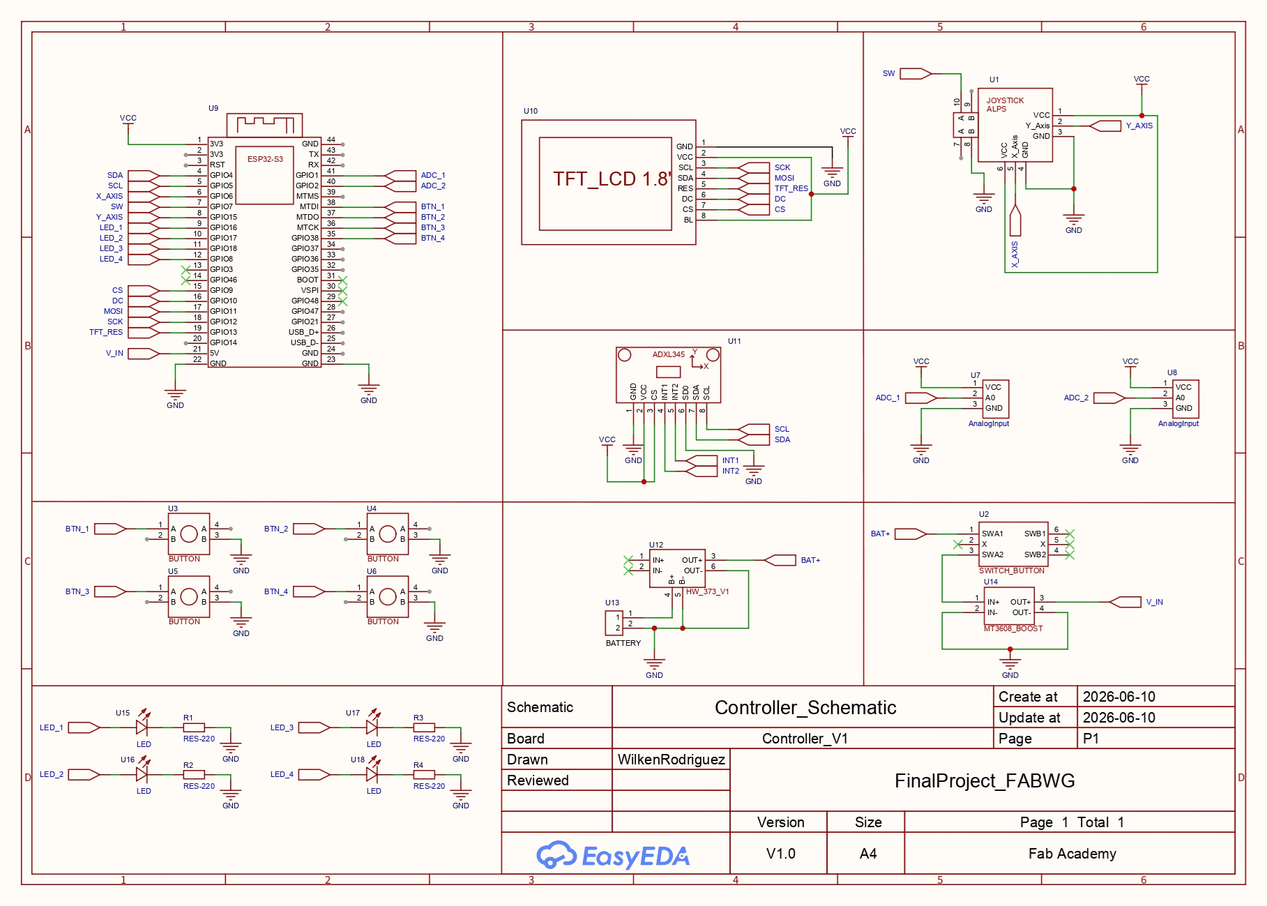
Complete electrical schematic showing the integration of sensing, display, power and user interface subsystems.
PCB Partitioning Strategy
The initial intention was to integrate the entire system into a single PCB. However, fabrication constraints imposed by the available FR-1 stock at the Fab Lab made this approach impractical. The available material sizes were limited to 10 × 10 cm and 15 × 10 cm boards, which introduced important space restrictions for routing and component placement.
Instead of increasing complexity or reducing functionality, the system was reorganized into multiple interconnected electronic modules. This decision preserved all planned features while simplifying fabrication and assembly.
Joystick Module
The analog joystick was implemented using a commercial joystick module connected through jumper wires. Since the joystick already includes its own PCB and mechanical mounting structure, reproducing the circuitry would have increased fabrication effort without adding educational value.
Using the existing module allowed the project to focus fabrication resources on the custom electronics while maintaining reliable analog input functionality.
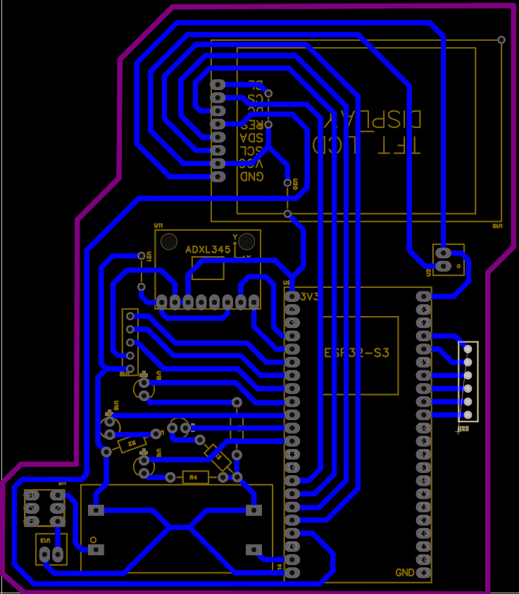
Main PCB integrating processing, sensing, display and power management subsystems.
Main PCB
The primary PCB acts as the central integration board of the project. It contains the ESP32-S3, the TFT display interface, the ADXL345 accelerometer module, the NeoPixel indicator, the four status LEDs and the complete power management subsystem.
The charging circuit is based on the HW-373 module connected to the 3.7V Li-Po battery. A power switch allows the system to be disconnected when not in use, while a boost converter provides the required voltage for stable operation.
This PCB functions as the processing and communication hub of the controller, coordinating all integrated peripherals and external expansion interfaces.
Secondary PCB
A second PCB was designed to host the user interaction elements located on the right side of the controller. Separating these components from the main board simplified routing and allowed the electronics to better match the physical layout of the enclosure.
This board contains the four multi-purpose push buttons used by the educational applications and demonstrations implemented on the system.
It also incorporates two dedicated GPIO expansion ports connected to the ESP32-S3. These ports provide direct access to ADC and touch-capable pins, enabling users to connect additional hardware without modifying the original design.
Through these connectors, users can interface buzzers, relays, analog sensors, LEDs, servos and motor control systems using external driver circuits such as H-bridge modules.
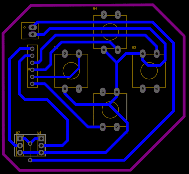
Secondary PCB containing the user buttons and GPIO expansion ports.
Integrated Electrical Architecture
Dividing the electronics into interconnected modules provided a practical solution to fabrication limitations while maintaining the original objectives of the project. The final architecture integrates processing, sensing, power management, user interaction and expansion capabilities into a cohesive embedded systems platform.
This modular organization also improves maintenance, debugging and future upgrades, reinforcing the educational nature of the GameLab Controller and supporting a wide variety of embedded systems learning activities.
3D PCB Visualization
In addition to the schematic and routing layouts, 3D PCB visualizations were used to verify the spatial distribution of components and evaluate how each board would fit inside the enclosure. These models provided an early validation of component placement, connector accessibility and mechanical compatibility before fabrication.
The main PCB concentrates the processing, sensing and power management subsystems, resulting in the highest component density of the project. The 3D model was particularly useful for verifying the position of the TFT display connector, the ESP32-S3 module, the ADXL345 accelerometer and the power management circuitry relative to the available space inside the controller housing.
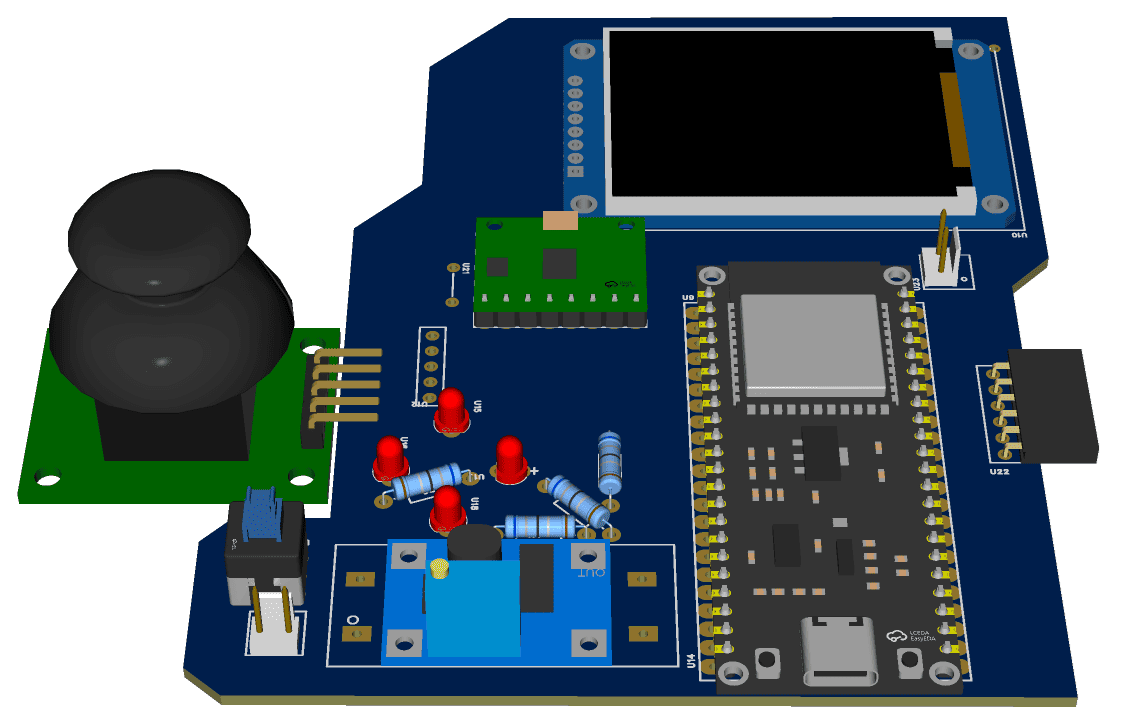
3D visualization of the main PCB showing the integration of the ESP32-S3, TFT display interface, IMU and power management subsystem.
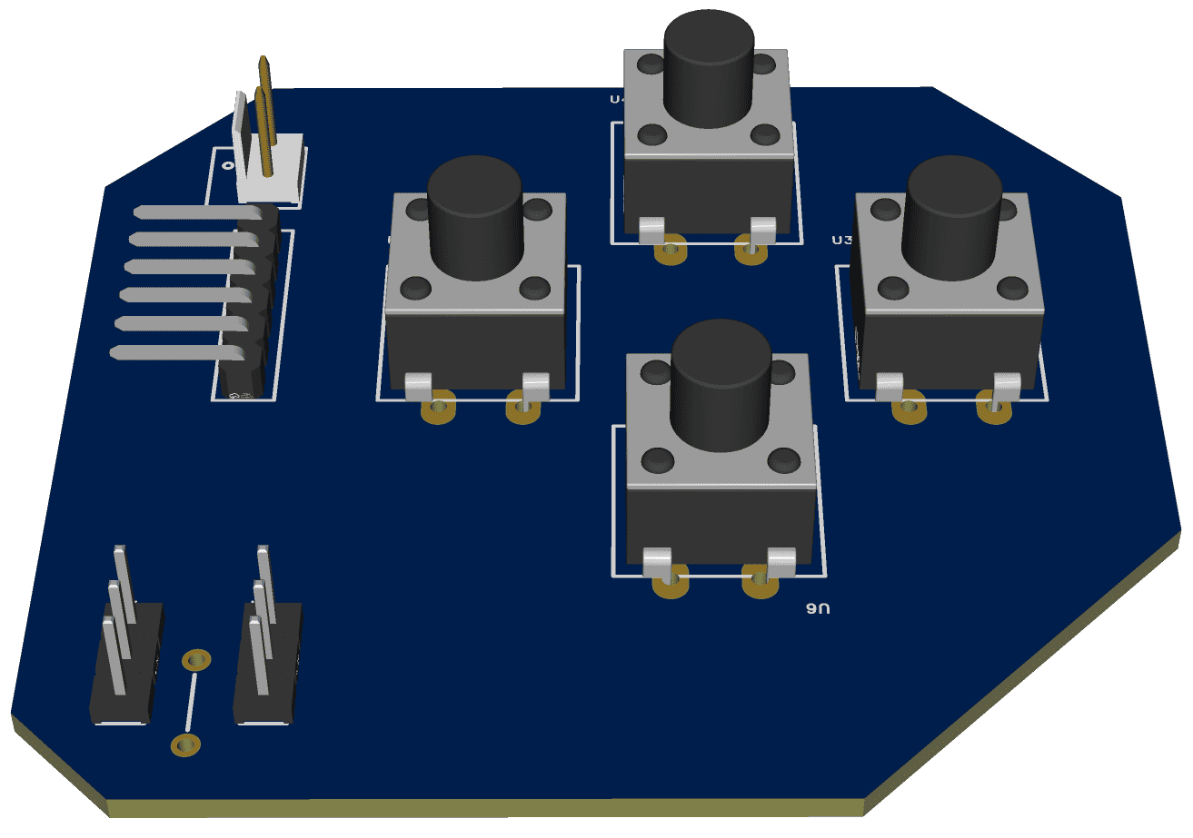
3D visualization of the secondary PCB containing the four user buttons and the GPIO expansion interfaces.
The secondary PCB presents a simpler architecture focused on user interaction and future expansion. The 3D model helped validate the position of the buttons relative to the enclosure openings and ensured that the GPIO expansion ports remained accessible from the exterior of the controller.
Together, these visualizations confirmed that both boards could be assembled as a single integrated system while maintaining accessibility, serviceability and compatibility with the mechanical design developed during the CAD integration stage.
Mechanical Packaging Strategy
Once the mechanical and electrical subsystems were designed, the final step of the integration process consisted of packaging all components into a single functional device. The objective of this stage was not only to place the electronics inside the enclosure, but also to ensure reliable interconnections, accessibility, maintainability and mechanical stability during operation.
Since the GameLab Controller was conceived as an educational platform, the packaging strategy needed to balance robustness with accessibility. The final assembly allows users to access the electronics, remove the ESP32-S3 module when necessary and connect external devices through the expansion ports while maintaining a compact handheld form factor.
Subsystem Interconnection
The complete system is composed of three main electronic modules: the joystick module, the main PCB and the secondary PCB. Each subsystem was integrated using a connection method adapted to its function and physical location inside the enclosure.
The joystick was implemented using a commercial analog module connected to the main PCB through jumper wires. This solution simplified assembly while preserving the mechanical structure already included in the joystick module.
The main PCB and secondary PCB were interconnected using right-angle header connectors. These connectors provided a compact, reliable and easily serviceable connection between both boards while minimizing the amount of wiring required inside the enclosure.
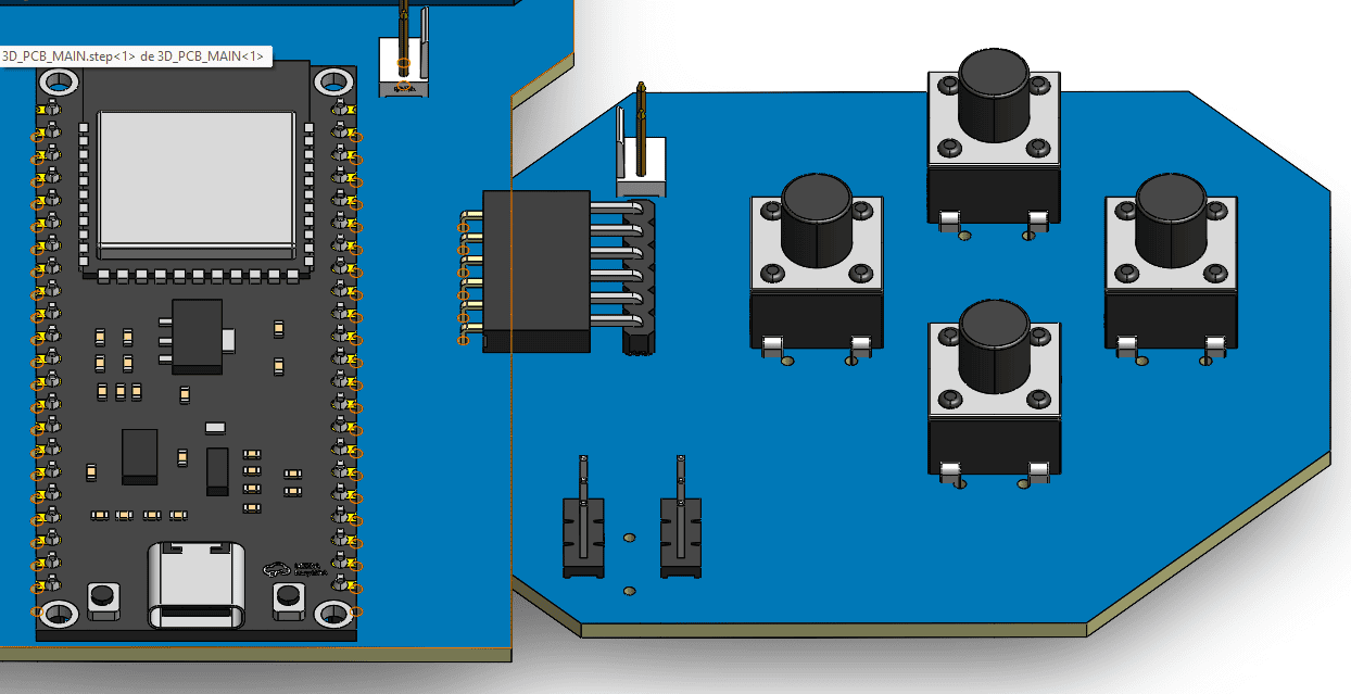
Internal interconnection between the joystick module, main PCB and secondary PCB.
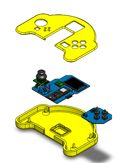
PCB mounting strategy and internal component organization.
Component Fixation and Stability
To prevent unwanted movement during handling, both custom PCBs were fixed to the enclosure using double-sided adhesive tape. This approach provided sufficient mechanical support while avoiding additional fastening hardware and simplifying assembly.
The use of adhesive mounting also helped reduce vibrations and movement that could generate intermittent electrical connections or mechanical stress on the solder joints.
The battery compartment, joystick module and interconnection cables were organized around the PCB assembly to avoid interference between components and maintain a clean internal layout.
Digital Assembly Validation
Before the final physical assembly, the mechanical and electronic components were validated in a virtual environment. The PCB designs were exported from EasyEDA as STEP models and imported into SolidWorks, allowing all subsystems to be assembled digitally.
This process made it possible to verify clearances, component positions, enclosure compatibility and assembly sequences before manufacturing the final parts. The digital assembly also helped identify potential collisions between the electronics, battery and enclosure walls.
The resulting virtual prototype provided a complete representation of the integrated system and served as a reference during the final assembly process.
SolidWorks assembly simulation showing the integration of all mechanical and electronic subsystems.
Final integrated assembly of the GameLab Controller.
Final Integrated System
The completed assembly combines the custom enclosure, joystick module, main PCB, secondary PCB, battery system and expansion interfaces into a single educational embedded systems platform.
All user interaction elements remain accessible from the exterior, including the TFT display, joystick, buttons, LEDs, GPIO ports and power switch. At the same time, the enclosure protects the internal electronics and maintains a clean and organized appearance.
The packaging strategy successfully transformed a collection of independent subsystems into a cohesive product capable of supporting learning activities in programming, electronics, sensing and embedded systems integration.
The final result demonstrates how mechanical design, electronics and assembly planning must work together to achieve a functional and maintainable embedded system.
Reflection
The System Integration stage was one of the most important phases of the project because it transformed a collection of independent ideas into a coherent educational platform. Although many individual subsystems had already been defined, this week required understanding how mechanical design, electronics, power management, user interaction and future expansion capabilities would coexist inside a single device.
One of the most valuable lessons learned was that system integration should not begin with the electronics, but with the user experience and the intended purpose of the product. In this project, the objective was to create an embedded systems learning platform that reduces the barriers commonly faced by beginners, such as wiring mistakes, component selection and circuit assembly. This educational objective influenced every design decision, from the selection of integrated peripherals to the inclusion of GPIO expansion ports.
Another important lesson was the impact of real-world fabrication constraints on the design process. The initial idea of integrating all electronics into a single PCB had to be reconsidered due to the available board sizes in the Fab Lab. Instead of reducing functionality, the design evolved into a modular architecture composed of two interconnected PCBs. This solution ultimately improved flexibility and simplified the internal organization of the system.
The integration process also highlighted the importance of maintaining a close relationship between mechanical and electrical design. Decisions made during the enclosure design directly affected component placement, PCB layout and assembly methods. Likewise, the electronic architecture influenced the internal structure of the enclosure and the accessibility of key components such as the ESP32-S3, battery and expansion interfaces.
Looking back, one aspect that could be improved in a future iteration would be the development of a custom joystick module and a more compact power management subsystem. These modifications would reduce the number of off-the-shelf modules and allow a higher level of integration. However, for an educational platform, the current design achieves a good balance between manufacturability, maintainability and functionality.
Overall, this stage demonstrated that successful embedded systems projects depend not only on designing individual components but also on carefully planning how those components interact as part of a complete product. The final result is a portable embedded systems laboratory that combines sensing, interaction, visualization and expansion capabilities into a unified learning platform.
Downloads
All downloadable resources required to reproduce the GameLab Controller are stored directly within this GitLab repository. The files include the mechanical design, PCB manufacturing files, source code, printing assets, and documentation developed throughout the project.
| Resource | Description | Format | Download |
|---|---|---|---|
| 🖨️ 3D Controller Design | Complete 3D CAD model of the controller enclosure and mechanical components. | ZIP | Download |
| 🎨 Printing Graphics | Artwork and printable graphics used for the controller labels and assembly. | ZIP | Download |
| 📄 Electrical Schematic | Complete schematic diagram of the custom PCB. | View | |
| ⚡ EasyEDA Project | Editable EasyEDA project containing the schematic and PCB layout. | ZIP | Download |
| 🏭 Gerber Files | Manufacturing files for professional PCB fabrication. | ZIP | Download |
| 💻 Arduino Programs | Source code developed for the ESP32-based controller. | ZIP | Download |
| ✂️ PCB Vector Files | Vector files used for PCB fabrication and laser/CNC workflows. | ZIP | Download |
All downloadable resources are included directly in the GitLab repository, ensuring long-term accessibility and compliance with Fab Academy documentation guidelines.