PCB Design with KiCad
KiCad is a free and open-source EDA (electronic design automation) software suite. Instead of a single software, it consist of connected softwares each with it's own specific function in electronic design pipeline such as schematic design, PCB layout, circuit simulation, etc. This post will only able brush upon small set of it's features. Watch this excellent intro to KiCad tutorials by DigiKey to learn KiCad more in depth.
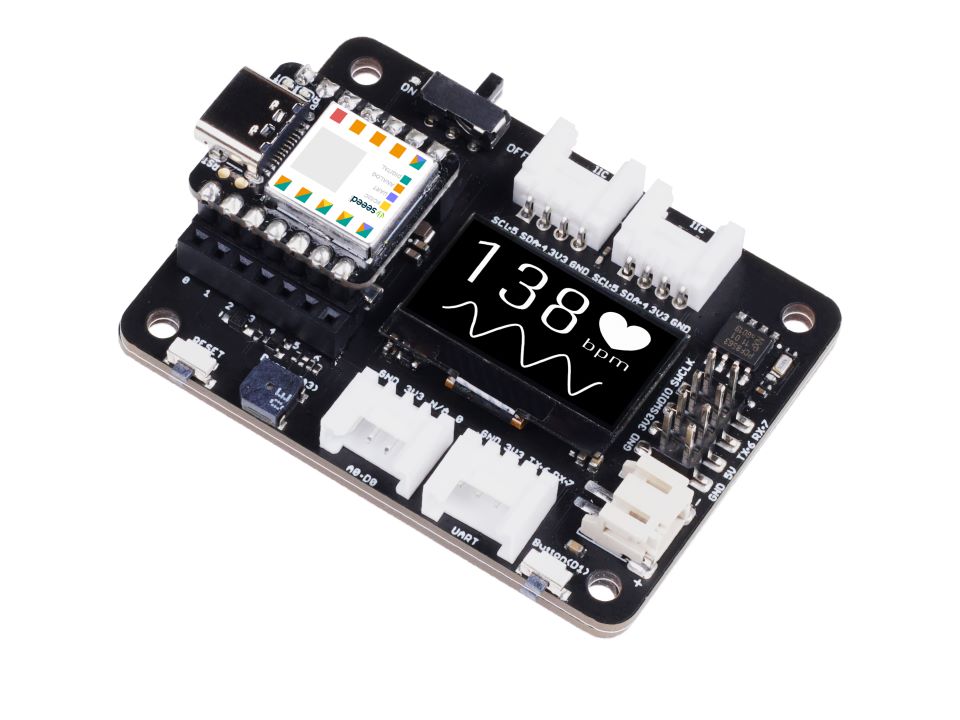
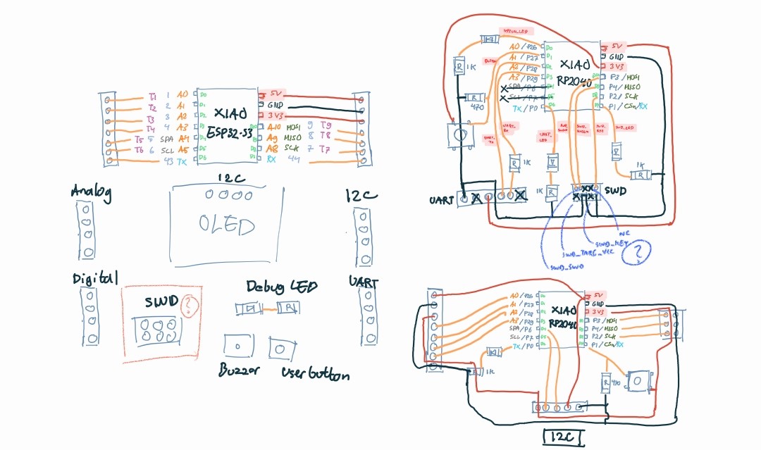
In this article we will be designing a development board that compatible with Seeed Studio XIAO series as it's MCU. The XIAO microcontroller series are powerful and pack with tons of feature in a tiny form factor. However, this form factor also become it's own limiting factor when we want to use multiple peripherals and quickly running out of pins.
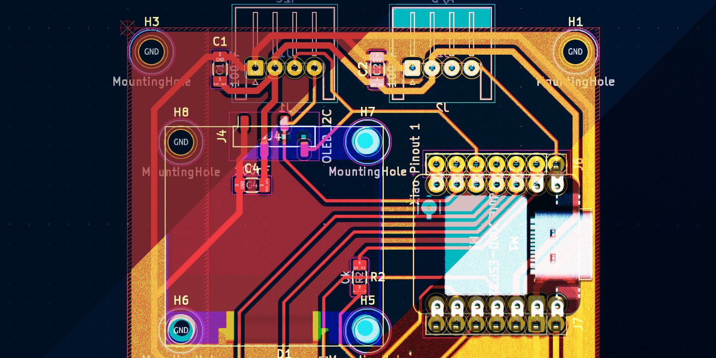
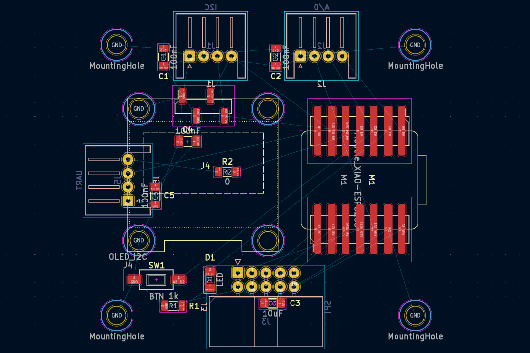
The development board will have a 0.98" OLED screen, a button, and a LED for debugging purposes. It has dedicated ports each for I2C, UART, and generic analog/digital protocol using JST connector; and a SPI port using IDC connector. Each of these ports are equipped with a decoupling capacitor to help stabilize the voltage level of each port. On top of that, there are accessible header sockets directly connected to each of XIAO 14 pins, making it a very flexible development board. This design is highly inspired by Seeed Studio's own Expansion Board with the distinction that it is design for a single layer PCB.
Installing Library
KiCad comes with tons of default libraries, however there are way more components out there and you can even make your own library. Fab Academy has it's own standardized components library for KiCad. To install it, follow the instruction below:
- Download this GitLab repository as a .zip file.
- Extract the kicad-master directory into a safe directory. The recommended location for Windows is the default KiCad libraries directory
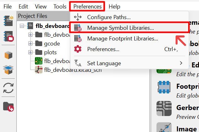
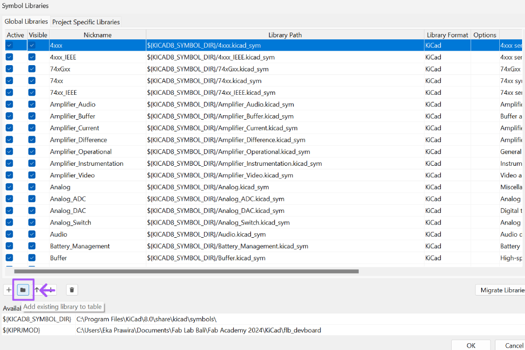
C:\Users\Name\Documents\KiCad\8.0\libraries. You may rename the kicad-master directory to something more descriptive like fab-libary. - Go to preference > manage symbol libraries. Click add existing library and select
fab.kicad_sym. - Repeat same process with preference > manage footprint libraries and add
fab.pretty.
Pre-Planning Your Design
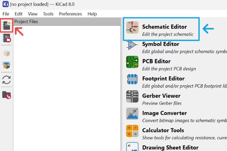
Before starting your design in KiCad, it is helpful to sketch out your design first in a drawing. This will help you visualize early on where your component should be, the number of components in your design, and most importantly whether you have enough pin or not. Once you have quite a clear idea with your design, we can start translating the sketches into a schematic and eventually PCB layout. Open up KiCad, create new project, then open Schematic Editor.
Schematic Drawing
Schematic is a simple visual representation of your electronic circuit. It shows all your components and their relation with each other using symbols and lines.
Symbol
To add a component, use add symbol tool (shortcut a), search and select it in the dialog box. Once selected, the symbol will be added to the sheet along with a reference and value. You can change them by double clicking and change their value.
To move the symbols, simply click and drag them. You can also reorient the symbol by selecting it, then rotating it by pressing r. Before you can make connection between these components, make sure you have change to add wire tool (shortcut w) or by simply exiting current active tool by pressing esc. Next, click one end of a component then one end of another component to create a connection.
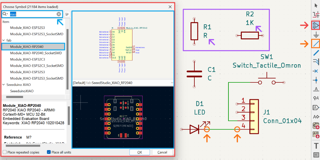
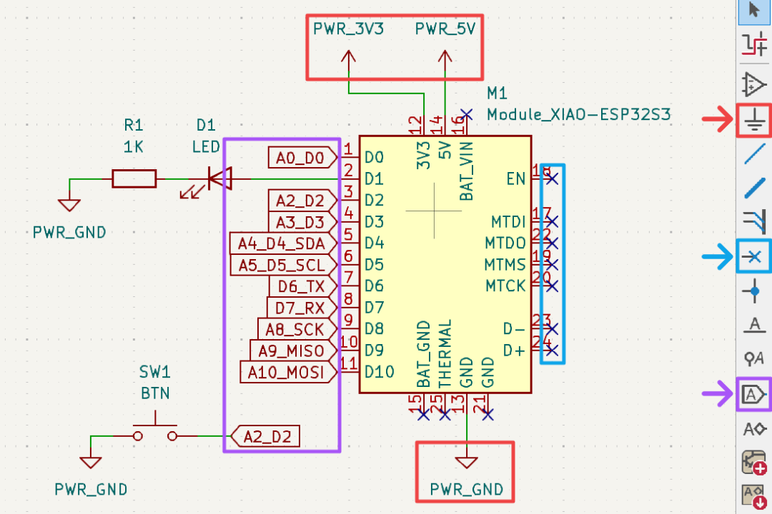
Beside components, you will also need to specify your power source in your schematic. Use add power tool (shortcut p) to add power symbol such as 5V, 3V3, GND, etc. If you have some pins that you won't be using, you will also need to add no connection flag (shortcut q) to those pins.
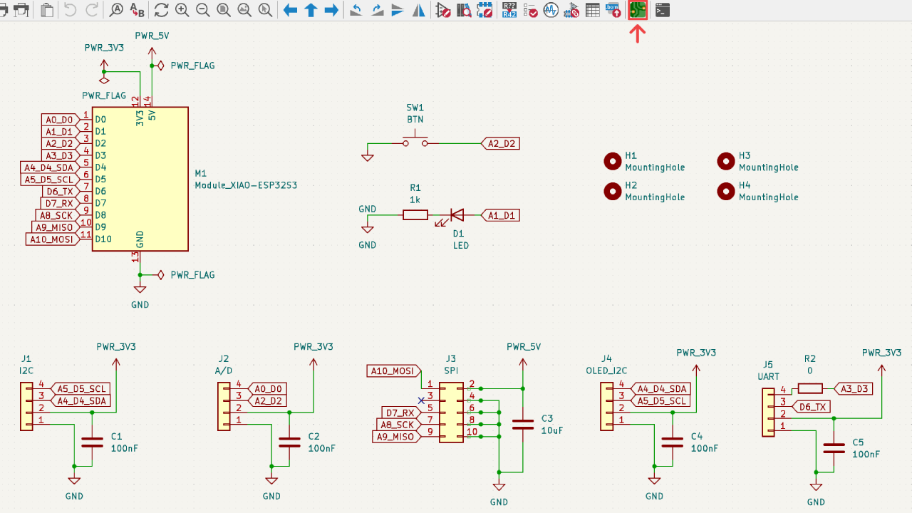
You can create your schematic by making a direct wire connection to all components like shown in the pin D1 below. However this will make the schematic unnecessarily complicated and hard to read. To simplify things, you can break up the schematic into multiple sub-system and add global label (shortcut ctrl + l) to represent the connection between them. See pin D2 below, where it was given A2_D2 label, and it connected to a switch button sub-system that connected to the same label.
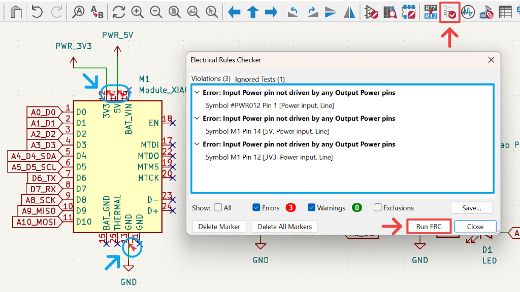
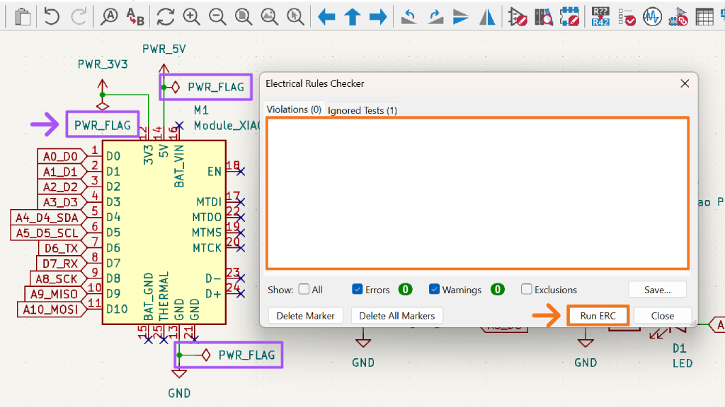
ERC
Once you have create all your system schematic, run ERC (electrical rules checker) to verify them. If there are any errors it will detail them in the dialog box and show them where the errors are in the schematic. In this instance, we need to add power flag to our power symbols. Run the ERC again to verify if all the errors have been fixed.
Footprint
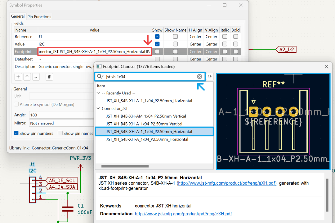
You may realized when we add the components, some of them already have a footprint assigned with them but some may not. A footprint is the physical layout of a component in a PCB consisting of pads/pins, marking, mask, etc. When designing a PCB based on your schematic, all the components need to have a footprint assigned. To do this, double click the component symbol and browse the footprint chooser. You can use the search dialog and select the footprint that you want to use for that component. You can also change a predefined footprint the same way, for example if you want to change a connector from vertical to horizontal type.
When you are ready to design your PCB layout, click the switch to PCB editor on the top tool bar. The workflow is not necessarily need to be linear, you will most likely going to go back and forth between schematic and PCB editor multiple times throughout your electronic design process.
PCB Layout
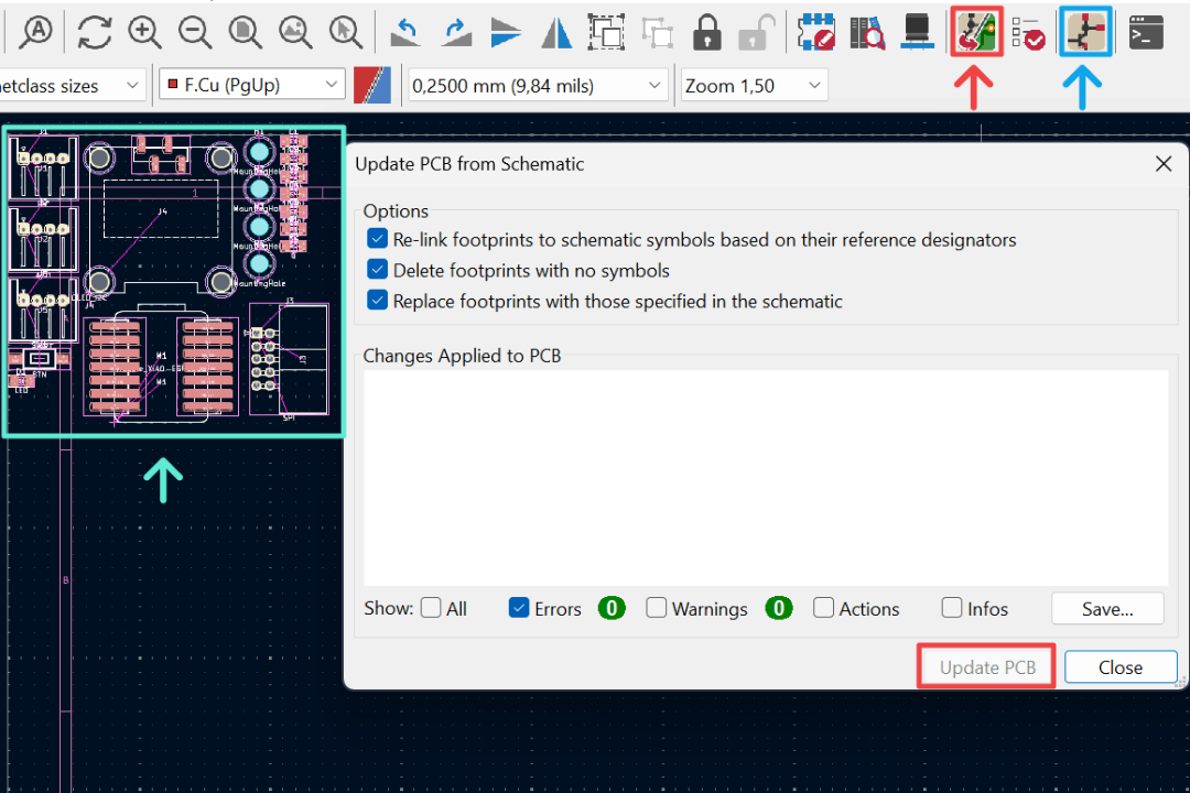
The first time you open your PCB Editor, it will be empty even when you already finished with the schematic. First thing you need to do is to run the update PCB from schematic, then click update PCB. This will update everything in the PCB editor to reflect any changes that you made in the schematic editor, in this case it will populate the editor with all our components footprints.
You can quickly go back to the schematic by clicking switch to schematic editor button. Remember to run the update PCB tool again whenever you did some changes to the schematic. Moving the footprints are very similar with moving the symbols, simply click and drag them, and press r to rotate them.
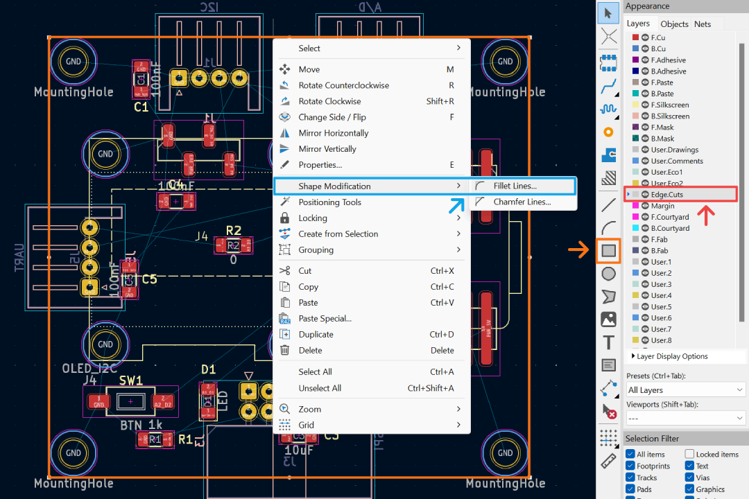
Edge Cut
Next we should create the border of our PCB. First, make sure you are in edge cuts layer. Create a rectangle using draw rectangle tool. By default this tool will be constrained to draw perfect square, however, you can freely resize it afterwards. For aesthetic purpose, you can round the corner by right clicking while the rectangle is selected, then select shape modification > fillet lines.
Design Rules
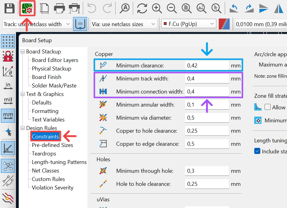
If you notice, there seems to be some random lines all over your footprints. These are called rat nest, which shows you where those pads need to be connected by some copper tracks. However, before adding tracks, let's define some design rules first. They are a set of constrains and specifications that we can define to ensure that our design are reliable and can be fabricated with our machine and milling bit.
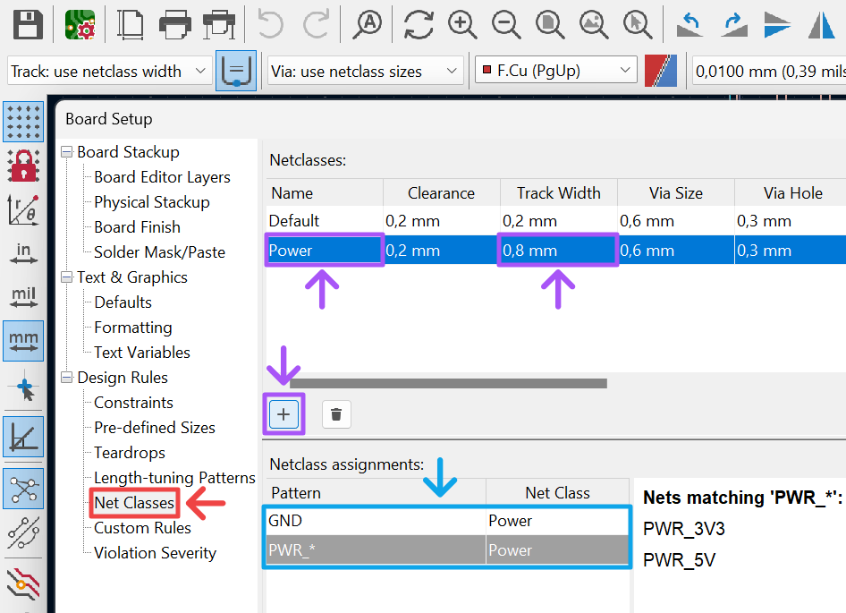
Go to board setup and choose constraints where we can find global values that will be used to help maintain consistency and prevent violation during the layout process for the whole board. By default the values for minimum clearance, minimum track width, and minimum connection width were 0. These value need to be adjusted depending of the milling bit we plan to use. If you use 1/64" straight end mill for isolating traces, you'll need to apply a value the same or slightly higher than the tool diameter (approximately 0.4 mm) as the minimum clearance value. Since we are using a cheap CNC milling such as 3018, let's add a little more safety margin and use 0.42 mm for minimum clearance. For the same reason, both the minimum track width and minimum connection width were given a conservative value of 0.4 mm.
Beside constraints, KiCad also define some net classes. Think of them as some preset for our tracks. By default KiCad has a default net class which has track width and clearance value of 0.2 mm. These values won't be applied to our tracks because they are lower than the minimum values we set as constraints. The track width will default to 0.4 mm and the clearance between the tracks will default to 0.42 mm. However, ideally we want a wider tracks for power lines compared to our signal lines because they will carry more current. Let's add new net class and name it Power. Next, set value of 0.8 mm for track width and we need to assign the power net class to their corresponding net pattern. In this case GND and all labels that start with PWR_. Close the dialog box and you are ready to add tracks for your board.
Tracks
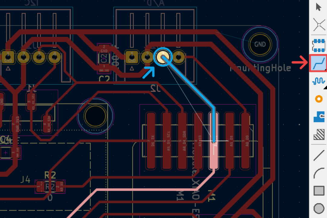
Select the route tracks tool (shortcut x) and start creating track by clicking from one pad to another connected one that indicated by the rat nest. Once a track has been defined, you can quickly refine them or even moving a footprint together with the connected tracks by hovering on top of them and press d.
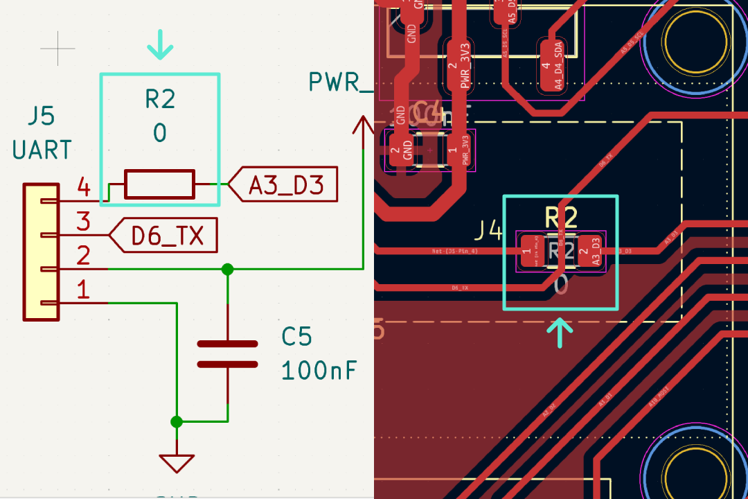
Keep adding tracks until all the rat nest disappear. If you find a track that simply impossible to connect because it got blocked by other tracks, consider adding 0 ohm resistor to jump past those tracks.
Ground Plane
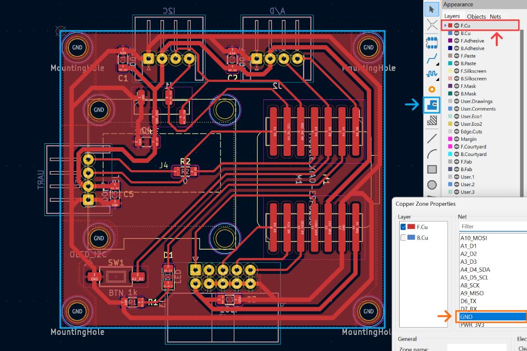
This design also employs a ground plane, where instead of the ground connected by a track like other pins, it use the rest of copper on the board as a plane connected to all the ground pins. It has many benefit such as reducing electrical noise and electromagnetic interference, improve heat dissipation and signal integrity.
To add a ground plane, first make sure you are in front copper layer, then select add filled zone tool, and start creating the bounding area of the zone. When you start first click, a dialog box will appear and you should select GND as the net class to be filled. After you finished drawing the area, press b to generate the filled zone. Whenever there are changes made to the position of footprints or tracks, you'll need to regenerate the filled zone again.
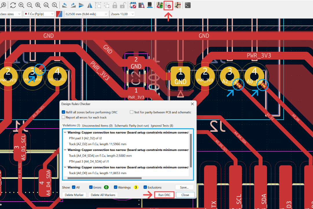
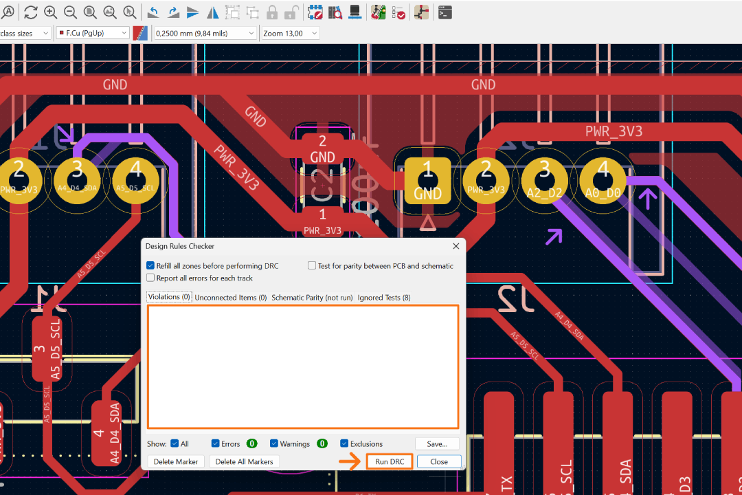
Just like schematic, you should also check your PCB design through DRC (design rules checker). It will analyze your PCB layout and shows any errors or warnings on the dialog box as well as the editor. Make all the necessary adjustments as recommended and run the DRC again to verify if the issues have been fixed.
Fabrication
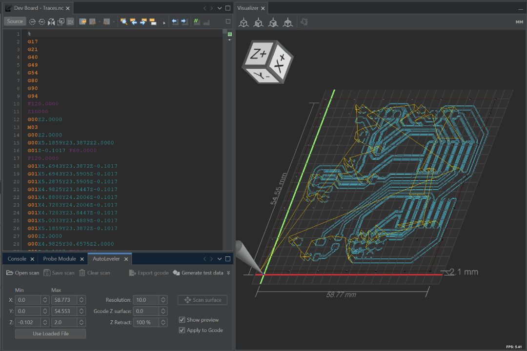
Once the design is completed, we can generate svg files for fabrication using plot tool. On the dialog box, make sure you tick all the layers you want to plot. In this case, we want to plot front copper and edge cuts layer. This design has some THT components, so we will need set drill marks to actual size. To make it easier when we generate the g-code in mods, tick the negative plot. Finally click the plot button to generate the selected layers into svg files.
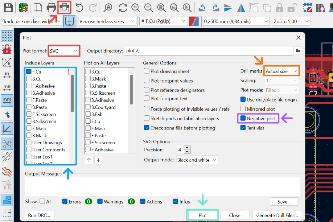
Using Inkscape, we can tidy up the svg files a little bit and separate it based on the milling operations. We need three files, one for isolation traces, one for drill holes, and last one for edge cuts.


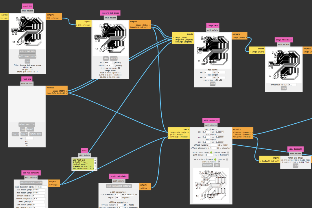
Below are the mods settings and milling bit we choose to fabricate this board. Parameters that not specified below were left as default. Generate the .nc files and mill your board following the same procedure described in milling Quentorres article.
| Traces | Drill holes & edge cuts | |
|---|---|---|
| Milling bit | 0.1 mm 20° v-bit | 0.8 mm corn teeth end mill |
| Tool diameter | 0.4 mm | 0.8 mm |
| Cut depth | 0.1 mm | 0.6 mm |
| Max depth | 0.1 mm | 1.8 mm |
| Cut speed | 2 mm/s | 2 mm/s |
| Plunge speed | 1 mm/s | 1 mm/s |
| Spindle | 10,000 RPM | 10,000 RPM |
Stuffing
Once the board milled, follow the same stuffing steps as described in milling Quentorres article to solder the SMD components. In short summary:
- Clean the PCB by wet sanding it using 800 grit sand paper and wash it using dish soap afterwards.
- Collect and labels all your components.
- Tin one pad for each SMD components using solder. Use flux generously to help the solder tin to flow easier.
- Stuffed the SMD components starting from the smallest in size. Use tweezer to hold component in place with one hand, remelt the pre-tinned solder pad, then solder the rest of the pins to it's pad.
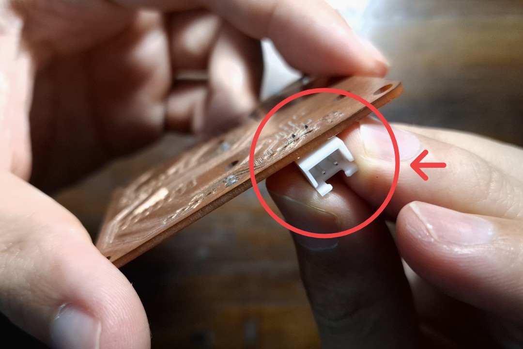
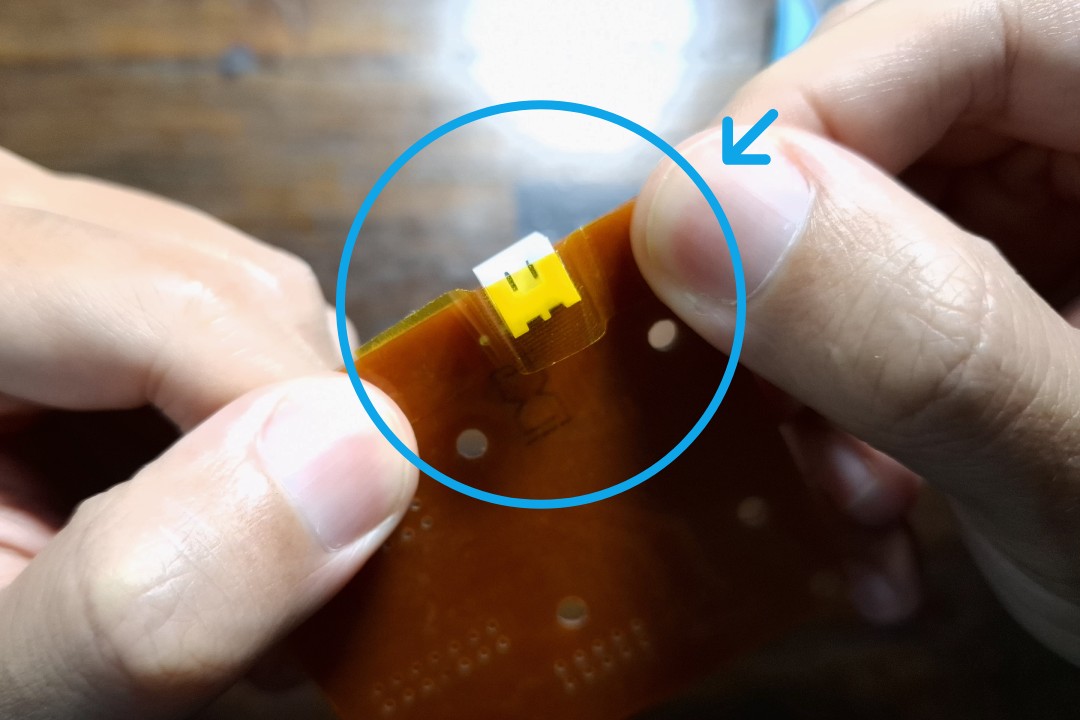
The THT headers generally are easier to hand solder compared to SMD components. However, there are things to be aware of to avoid some common mistakes. Depending on the size of the holes, the header might have a little play. If we accidentally solder them without proper alignment, it will be tricky to rectify especially if the header has a lot of pins. We can't use a breadboard like when we solder the XIAO headers, so we need another a way to keep the header in place. We can use a kapton tape (heat resistant tape) to do so while we solder all the pins on the other side.
Upload a Program
Once the stuffing is done, upload a sketch to test the functionality of the board. The sketch for demo below will be discussed in detail for the coming output device assignment.