III. Redraw an echo hello-world board
For redrawing an echo hello-world board, I chose the ATtiny45 version.
I’ve made it with Autodesk Eagle 9.6. Eagle is also implemented in Fusion360. I’ve tried this version, but it was very slow and after two crashes, I switched back to the “standalone” Version of Eagle.
There are a few tutorials available on the internet. Many of them are outdated, but they have still some useful information.
These are the tutorials I’ve red to see, how Eagle works.
https://maker.pro/custom/tutorial/autodesk-eagle-for-beginners-basics
https://www.build-electronic-circuits.com/eagle-autorouter/
https://www.sparkfun.com/EAGLE
https://sienci.com/2018/08/23/pcb-milling-tutorial/
During the assignments, I’ve also tested KiCad and documented it in my Input devices week.
I’m more comfortable with KiCad, so I prefer to use it in the future.
Drawing the Schematics
For first testing, I redraw the ‘original’ Hello-World Board, starting with drawing the schematics.
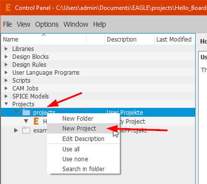
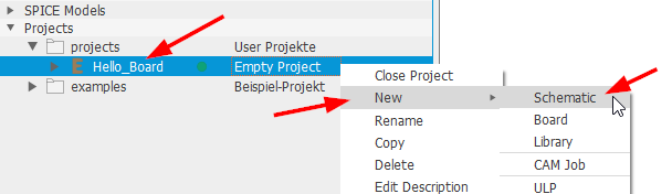
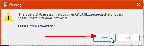
After starting Eagle, the Control Panel pops up. There I’ve to create a new project and then create a new schematic.
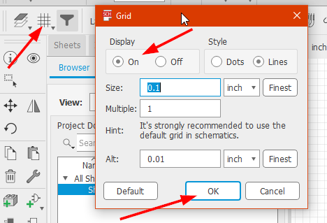
In the schematic Editor I enabled a grid.
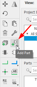
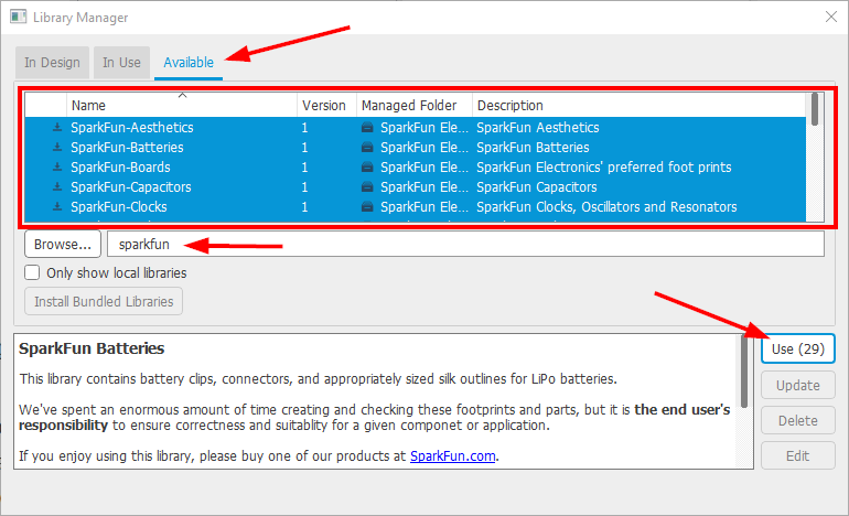
By clicking the add parts button, a new window appears. There I’ve added the sparkfun libraries first
Then I’ve started adding and placing the parts.
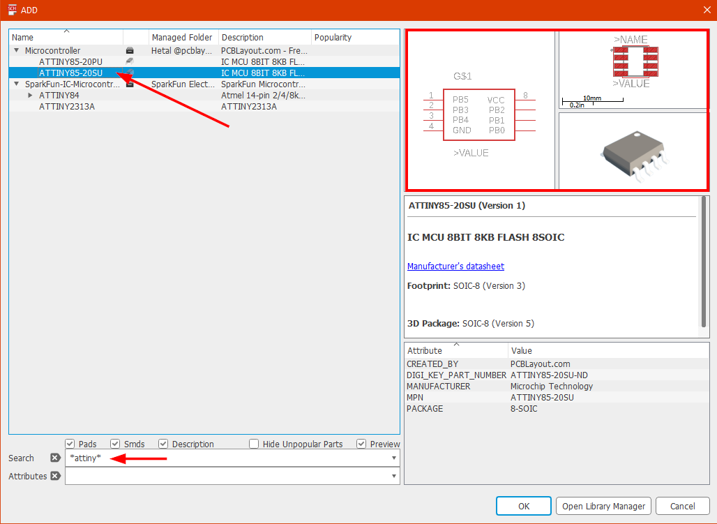
It’s very important to choose the right components,with the correct Footprint
Otherwise, the components you have, will not fit on the board.
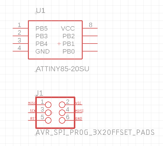
I’ve added these parts :
- ATTINY85-20SU (Version 1)
- 4x GND (Version 1)
- 4x VCC (Version 1)
- 6_PIN_SERIAL_TARGETSMD (6_PIN_SERIAL_TARGET) (Version 1)
- 2x RESISTOR0805 (RESISTOR) (Version 1)
- 1.0UF-0805-25V-10% (1.0UF) (Version 1)
- CONN_03X2FEMALE_SMD (CONN_03X2) (Version 1)
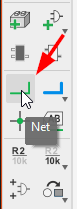
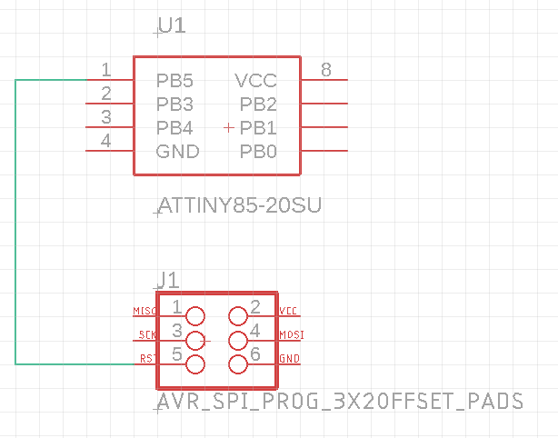
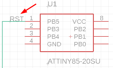
With the net icon, the parts have to be connected
With the name icon, the net-lines can be named.
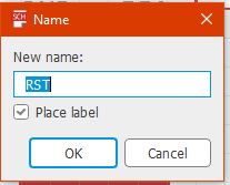
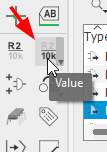
I used standard resistors with no values. The values can be set by clicking the Value Icon
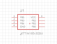
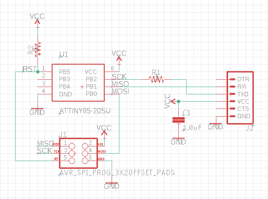
And that’s how my schematic looks like
creating the board
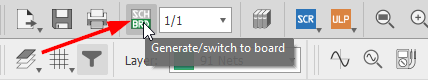
Next step is creating the board layout by clicking the Generate/switch to board icon.
All parts a nested in the bottom left corner
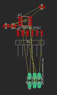
The parts can be arranged just by drag an drop and they can also be rotated.
The yellow lines are air wires and shows, which parts are connected.
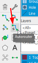
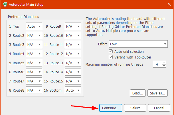
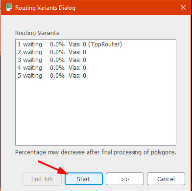
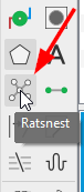
These air wires can be routed automatically by clicking the Autorouter icon.
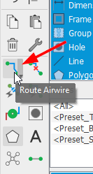
Or they can be routed manually
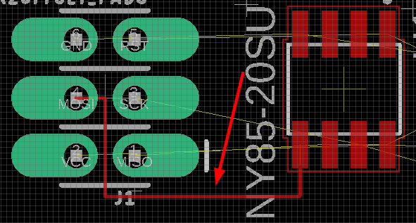
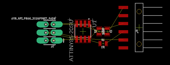
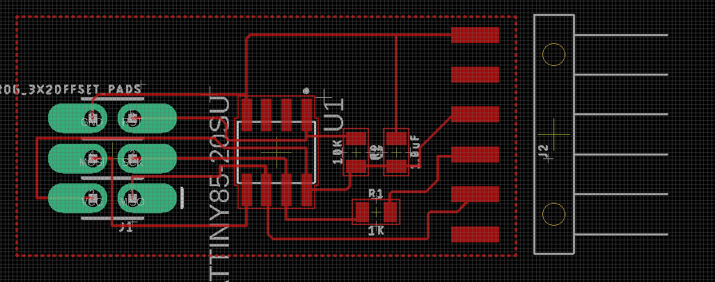
After connecting everything, my board looks like this
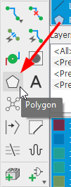
With the delete icon, I’ve deleted the yellow border.
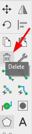
and drew a new polygon around the board.
The new polygon outline can be named GND
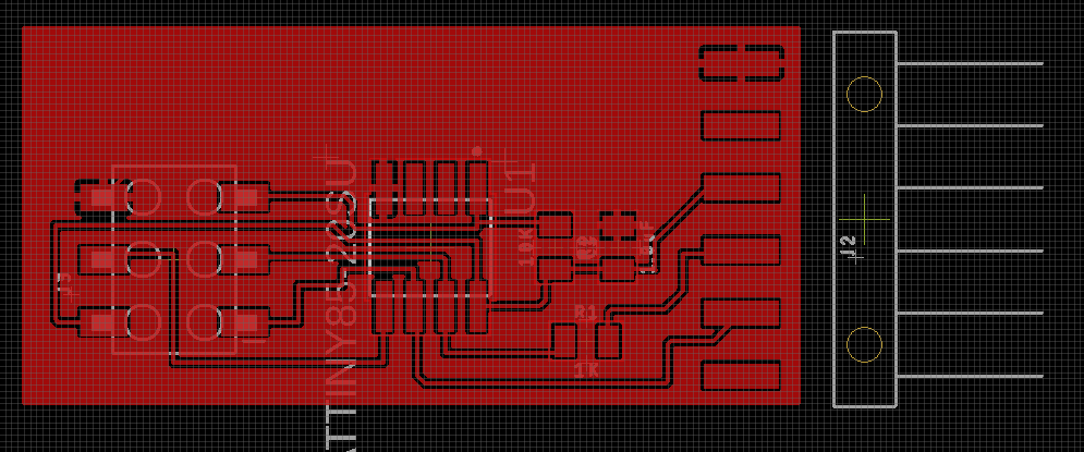
And then with the Ratsnest icon, the ‘free’ space on the board, will be converted as on big GND trace.
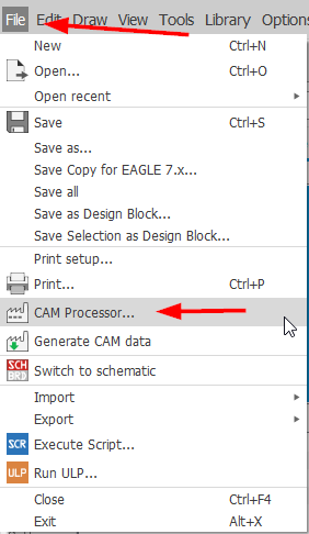
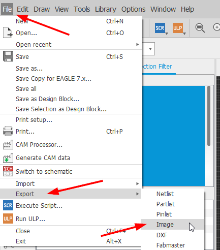
With the cam processor the gerber files can be created. These a necessary for the pcb manufactory.
redraw and adding components
To solve the assignment, I draw a new schematic with the following components.
CONN_03X2FEMALE_SMD (CONN_03X2)
4x GND (Version 1)
3x VCC (Version 1)
ATTINY45TINY45-20-SMT (ATTINY45)
3x RESISTOR0805 (RESISTOR)
6_PIN_SERIAL_TARGETSMD (6_PIN_SERIAL_TARGET)
1.0UF-0805-25V-10% (1.0UF)
B3SN-3012P
LEDCHIP-LED0805 (LED) (Version 10)
Adding the Omron B3SN-3012P push button was a bit tricky.
I had to signup at SnapEDA and got the footprint of the pushbutton there
After downloading, the library has to copy to the Eagle / libraries folder.
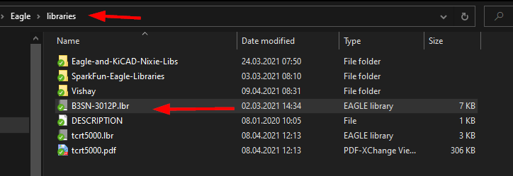
The standard path in Windows is %USERPROFILE%\Documents\EAGLE\libraries
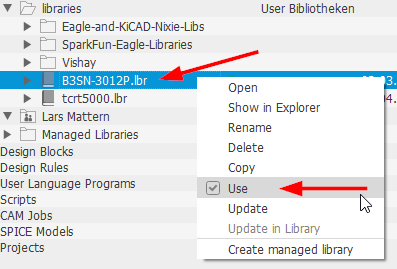
In Eagle Control Panel open the libraries folder, right click on the downloaded library and mark use
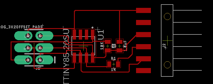
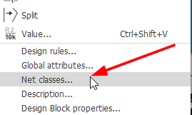
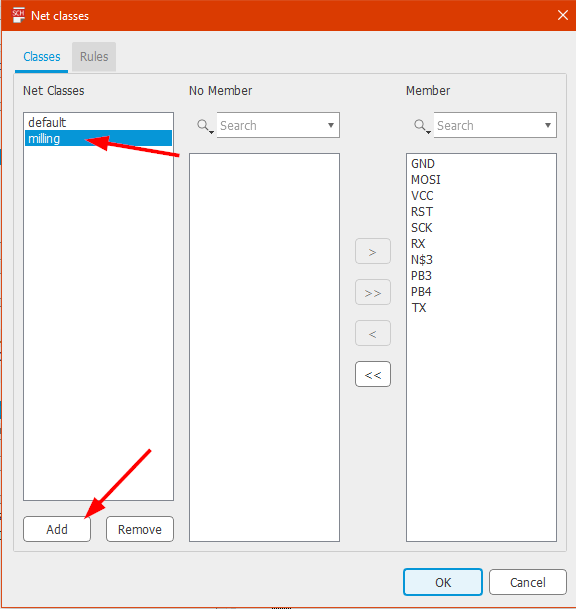
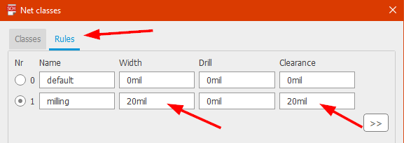
I’ve also added a custom net class, that I’ll get bigger traces, in the Board Editor.
This is my schematic, after adding and netting everything together.
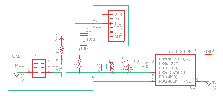
Surely it could be look better. I need more practice for that.
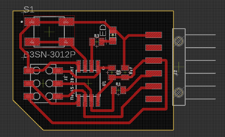
This is my board after placing and routing
DRC Check
For milling I would say, the more bigger the traces and the more bigger the space between them, the more better :D
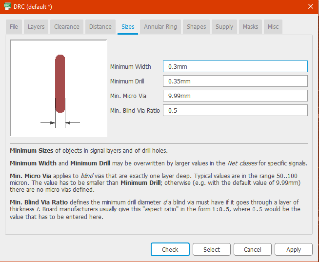
In my machine, I use a 0.4mm end-mill for milling the traces. This means that the minimum distance between two tracks MUST also be at least 0.4mm.
I made the experience, that traces, smaller than 0.4mm could make problems, in my cheap CNC3018.
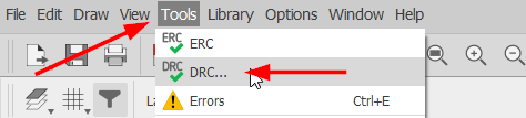
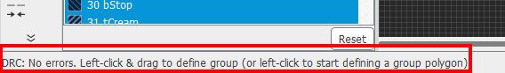
For the Design Rule Check, we click in the menu on Tools - DRC
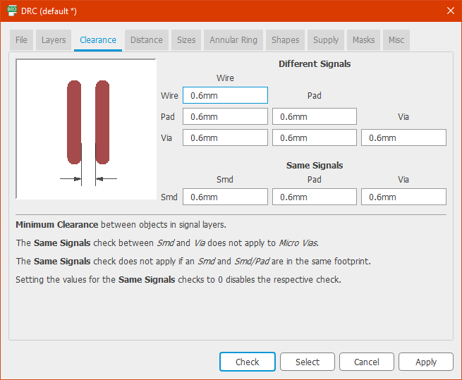
In the Clearance tab, we can define the minimum distances between Tracks and Pads etc.
I set everything to 0.6mm here
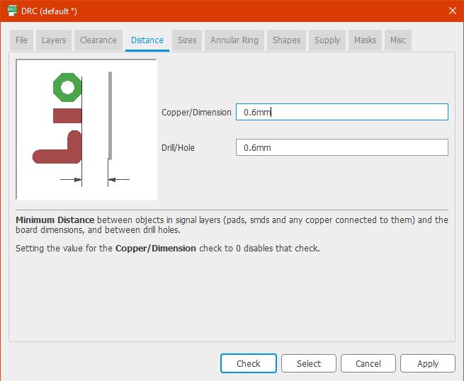
Same with the Distance Tab
In the Sizes Tab, the Track-Width can be defined. I set this to a minimum of 0.3mm
With a click on Check the DRC starts.
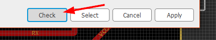
And when everything goes well, a message in the bottom status bar appears
export png
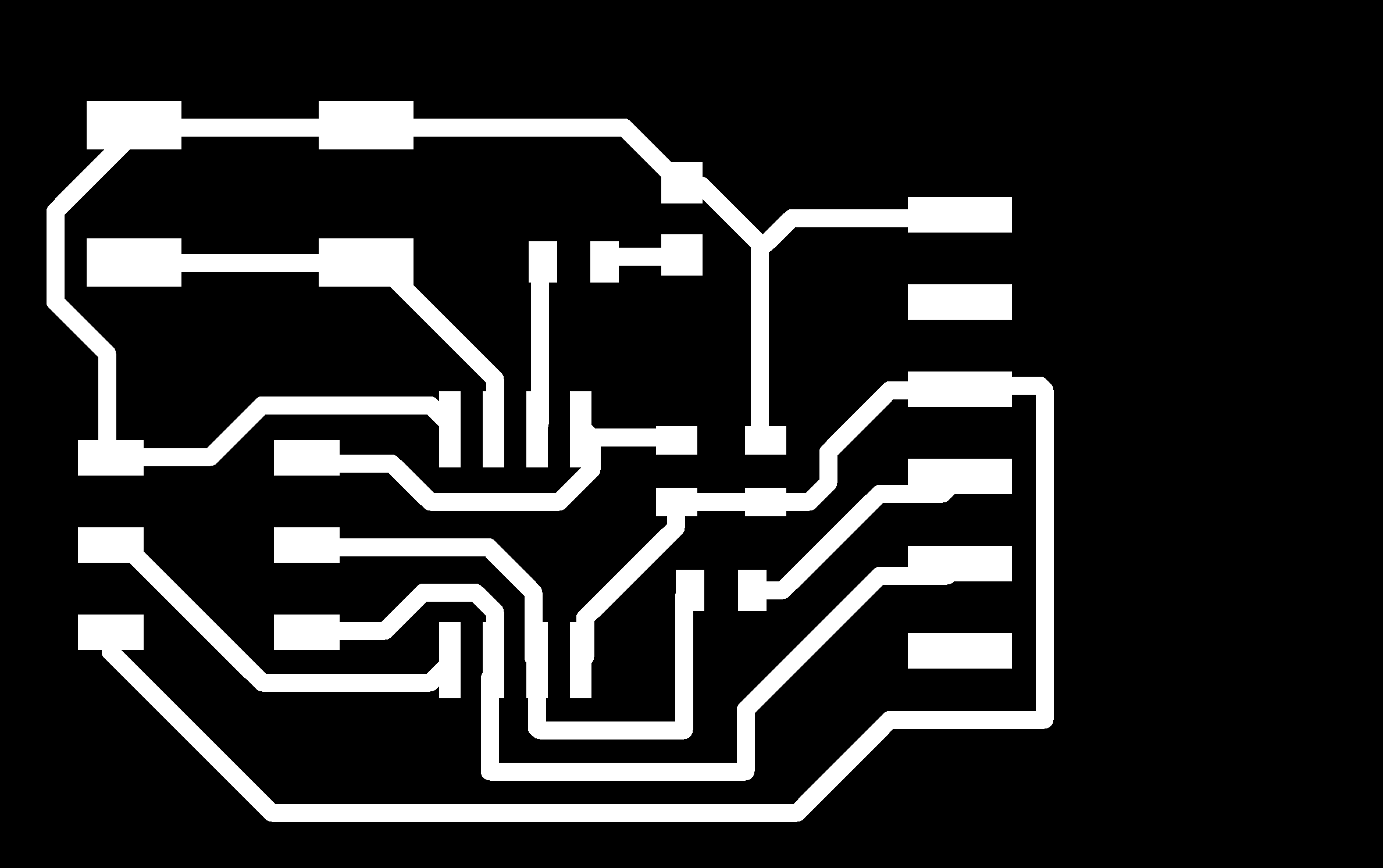
For milling we need to export two png files. One for the traces and one for the outline.
First we go into the Layer Settings and disable all layers except the Top
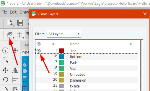
The board should now look like this
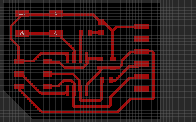
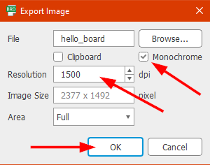
In the next step, we export the board as an image
In the window we change now the resolution to 1500 dpi, check the Monochrome option and choose a file name
After exporting we have the png with the traces
For the outlines we go again into Layer Settings and enable only the Dimensions Layer
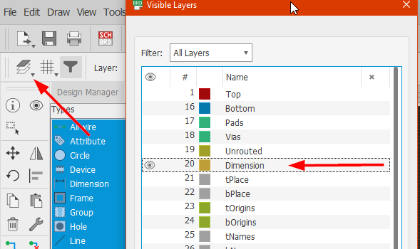
After changing, only the outlines are now visible
Now we have to export this also as an image, with the same settings as above.
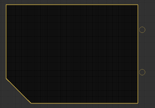
After exporting, the image looks like that.
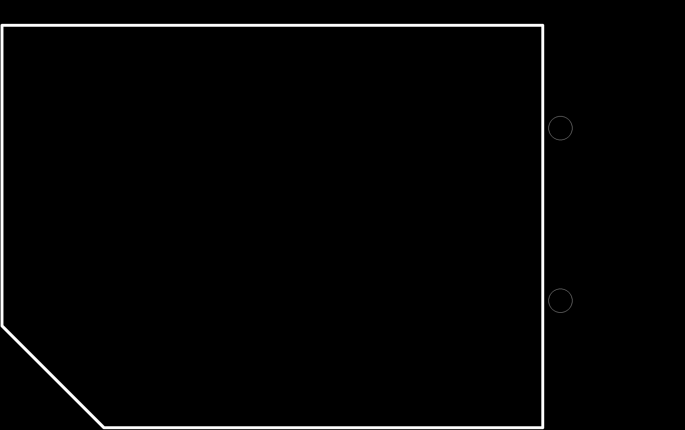
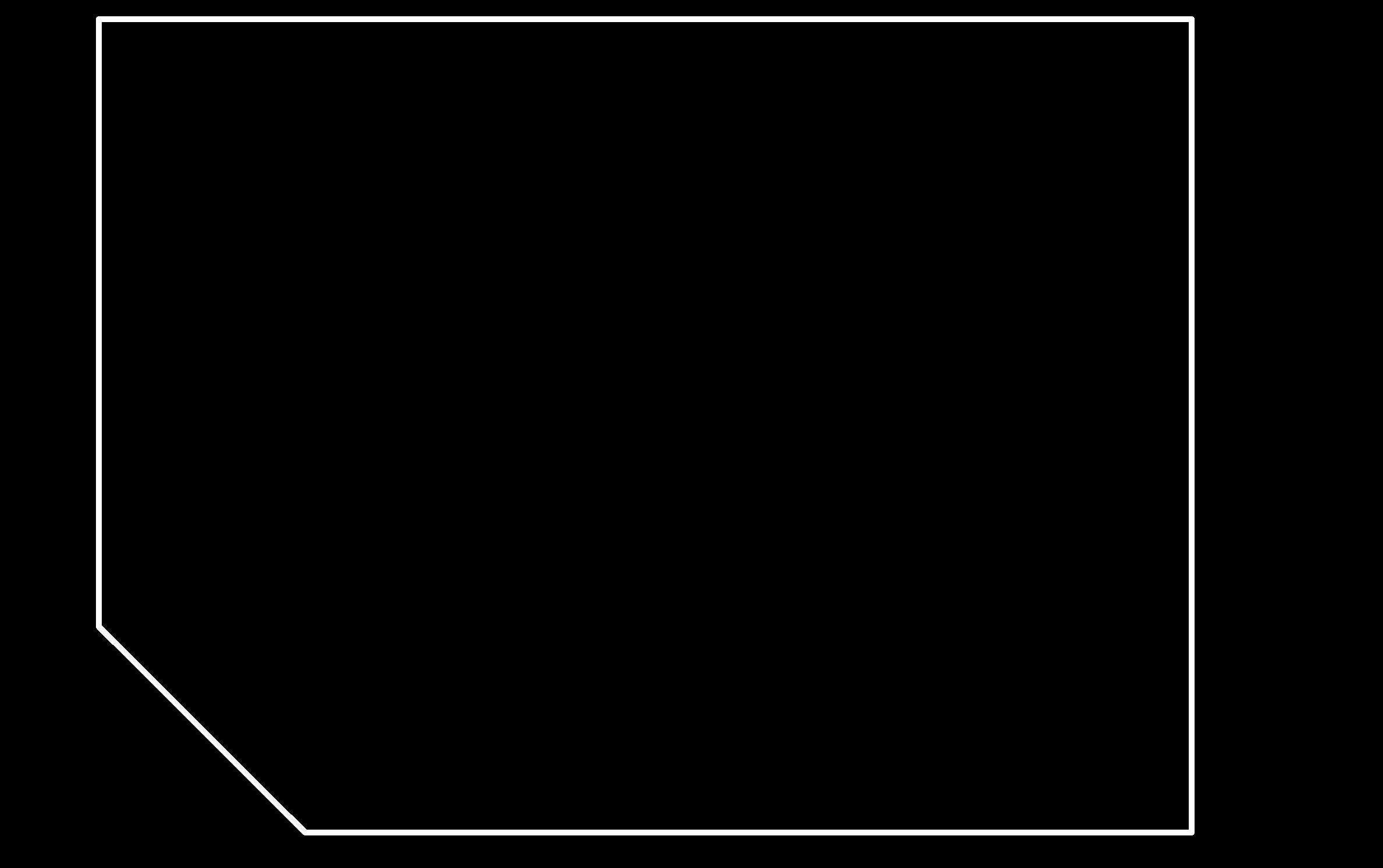
I had to edit the file, because I don’t need the two holes and the outlines are too close to the edge. For editing I just opened the file in MS-Paint and draw black filled squares over the two holes and moved the Outlines more in the middle.
The finished file looks now like this
My Eagle files can be downloaded here