EDA Design - Seeed Studio XIAO
To prepare for my final project, I originally planned to make a simulation of my project circuit.
Unfortunately, I ran out of time to create a fully working Solonoid circuit with a capacitor and a mosfet, so my instructor Mr. Dubick told me to just design a simple LED circuit with a resistor and a push-button as the switch.
KiCAD
Simulation
First, I created a simulation of a simple button press on the rp2040.
The simulation in Wokwi was kind of unreliable because of severe server lag. The time delay was extreme and whenever I clicked the button, the LED will sometimes light up. If I click it too quickly, it would just suddenly light up, and then the light disappears again.
Back in week 4, I already had the Pi Pico working with the push button and the LED with the exact same wiring and code.
Below is the simulation I made using an RP2040 Pi Pico using Wokwi:
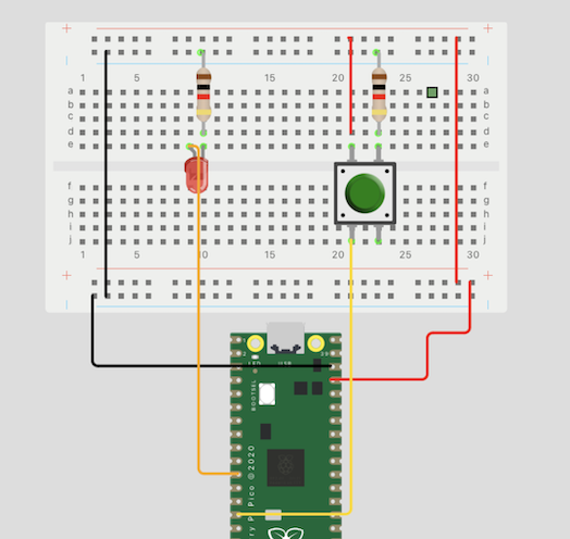
This time, however, we are using a slightly different device that still carries the same RP2040 microcontroller.
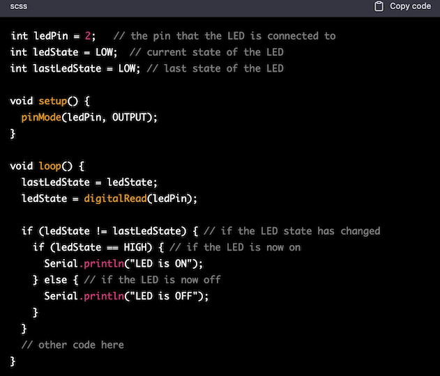
I asked ChatGPT for a simple code segment, and I found that it worked pretty consistently:
Next, I built this exact same circuit using physical hardware.
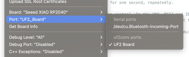
The port and board acted the same way as the Pi Pico controller in the Arduino IDE:
Then, I incorporated the Seeed Studio library into the Arduino IDE to test it out, using this website.
However, when I tested the button input, it didn’t work because the button keeps shorting the circuit.
Dylan found out that it was because the resistor and the ground wire are at the same place, and that I have to put the resistor in the actual ground port on the long side of the breadboard for it to work, or else electricity would go through the path of least resistance and short the circuit:
Here is a video of it working:
EDA Design
I designed my circuit in KiCAD, a simplisitc EDA design software.
Using this website provided by Mr. Dubick, I installed the Seeed Studio SAMD21 in the KiCAD software.
I followed the instructions in the website, successfully bringing in the schematic symbol for the Seeed Studio board and its pcb footprint. When the footprint did not immediately open, I quit KiCAD and restarted it, and it seemed to work.
As I was working on the circuit in eeschema, at first I couldn’t update my pcb from the schematic, but then I searched this problem up on Google and it said that I have to open my schematic file and pcb file from the .kiCAD_pro file link inside my folders, instead of using the individual .sch and .pcb files that are not inherently connected.
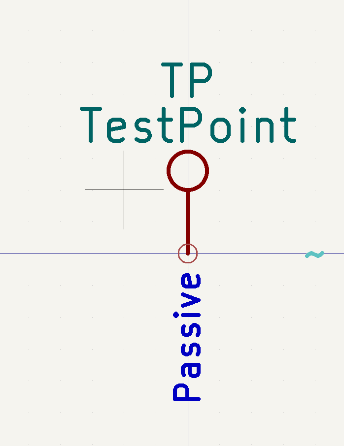
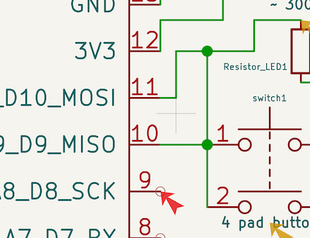
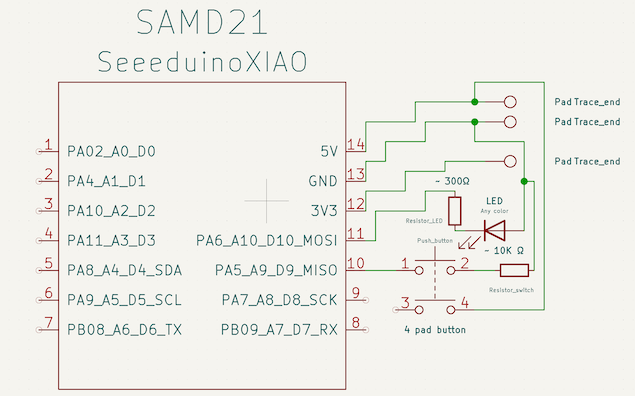
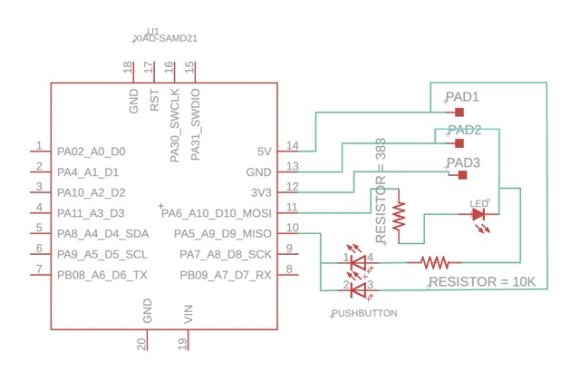
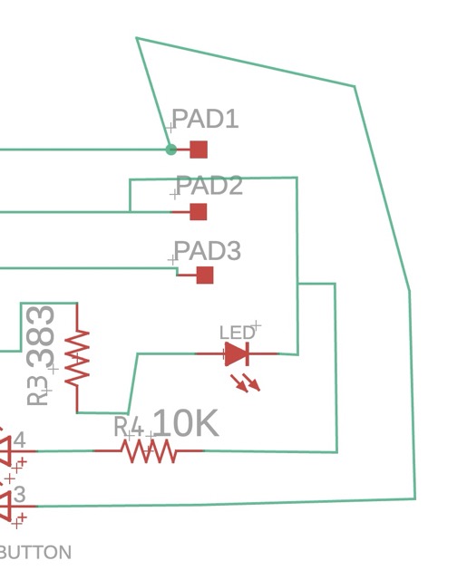
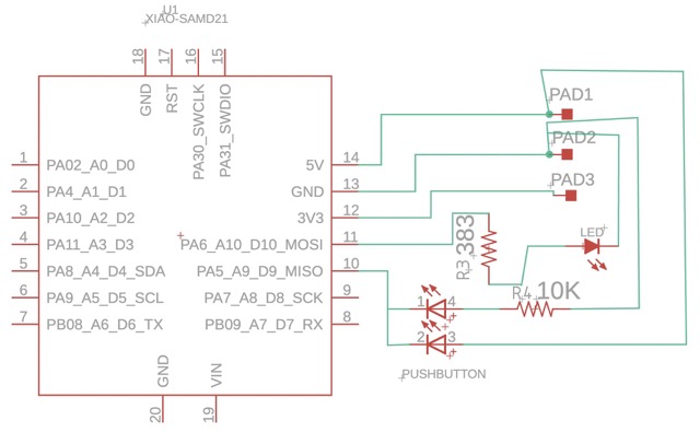
So, then I built my schematic, making sure to do use the pull-down resistor like Mr. Dubick taught me.
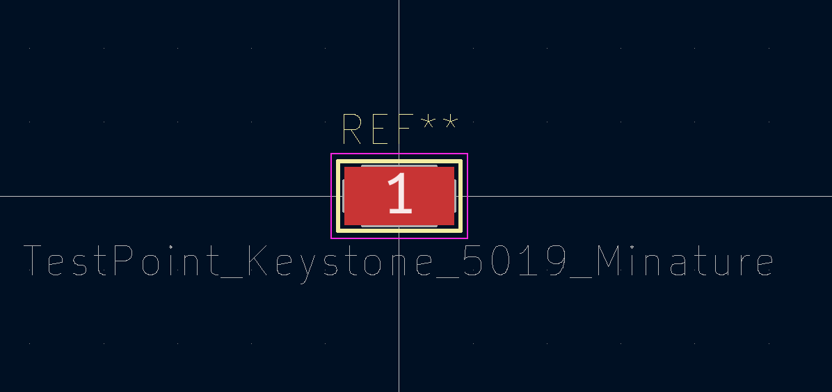
For additional components, I first need to find the right part in the component library in eeschema, such as this flat pad:
This pad is used to solder on male header pins that would be connected with female jumper wires.
Then, I must find the corresponding pcb footprint:
It took me a while to connect all the traces together because some of them just won’t connect – due to errors made in the schematic. So, after making sure that everything got connected together in the schematic, I updated the pcb again.
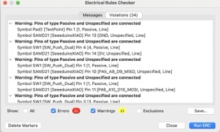
I used the Electric Rules Checker (ERC) to see my errors, such as this one in which there is an error in the connection:
When I import the eechema file into the pcb editor, the software automatically fixes the errors.
I checked the edits that the software made, and one of them is this:
Removed unused net unconnected -(SAMD21-PAD10)
This caused the pcb editor to remove the pad 10 connection:
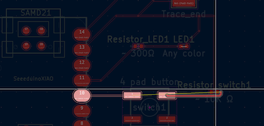
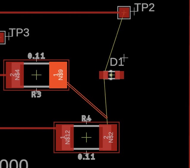
I solved the problem when I made a connection from the pad 10 to pad 11 in eeschema, this allowed me to make a trace from pad 10 to one of the button pads in the pcb editor.
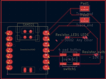
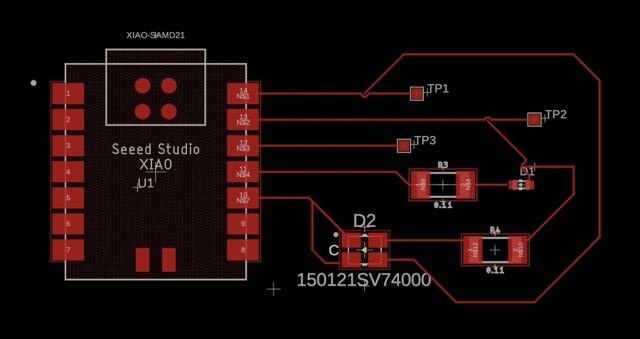
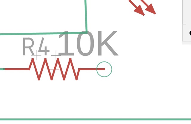
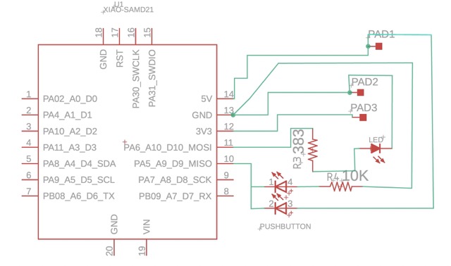
Here is my finished circuit:
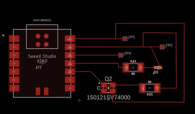
Here is the PCB design with all the connections:
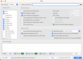
To export the design, I followed these instructions.
This is the plotting interface in KiCAD used to export the file for cutting:
Eagle
Next, I designed the exact same circuit in Autodesk’s EagleCAD, which is included in Fusion 360.
First, from this github repository, I downloaded the zip file containing the schematic and pcb footprint of the Seeeduino. This tutorial helped me to setup the Electronics file in Fusion 360, which is in the dropdown menu under File.
Then, the schematic editor was created. I clicked switch to pcb in order to create the pcb editor.
This is the Seeeduino schematic:
 .
.
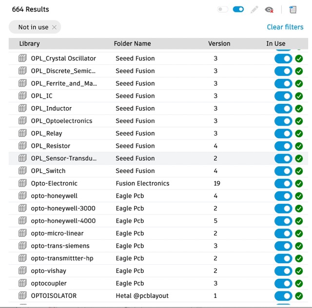
After clicking on the “add pcb components” button, I navigated to the library of components. However, I had to check over 800 libraries in order to activate them all:
Otherwise, I cannot use certain components. I wired the schematic similar to my KiCAD schematic:
 I also put on labels for each component.
I then switched to the PCB editor and found that the resistor’s footprint was wrong:

So, I went back to the schematic editor and switched it for a surface mount-soldered resistor.
However, some of the routing won’t snap on to the footprint pads properly, and some don’t link together at all:


I figured that the issue was in the schematic, and I realized that I needed to specify the connections between each component. For instance, the circle shown here mus show up when my mouse hovers over it:
Then, if I connect this resistor (shown above) to another component, it will be connected in the pcb editor, as reflected by this yellow line:
As shown above, the routing can now snap on to the footprint pad.
I updated my schematic editor, so now that the green circles indicate that the components are properly connected:
After rearranging the wires and making it look good, here is my final schematic and pcb diagrams:
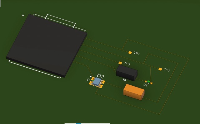
In the PCB editor, I switched to 3D view, which allows me to see a 3D render of my circuit:
Comparison
I have several insights regarding the similarities and differences between KiCAD and Autodesk Eagle:
- The eeschema editor in KiCAD allows for easier labeling as a double click is all that is needed. On the other hand, the requirement in Eagle to edit the attributes of each component makes it more difficult than it needs to be.
- Eagle has better flexibility in routing the circuit in the pcb editor, as it offers a variety of different routing types, including line, freeform, etc.
- KiCAD’s schematic and footprint library is better when checking for dimensions and variety. Their libraries open up in a separate window, which allows for easier viewing. Eagle’s library needs to be manually checked and its not clear at all the dimensions of each footprint.
- Eagle’s addition of a 3D view is better than KiCAD’s 2D only views. This allows you to incorporate the 3D circuit with a 3D design, allowing you to see how the board would fit.
- KiCAD’s error checking tool is superior to Eagle, which don’t have one.
- Eagle, on the other hand, has a simulator (which I haven’t figured out how to use yet) that KiCAD doesn’t have.
- KiCAD is open source, Eagle is not.
Soldering
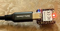
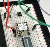
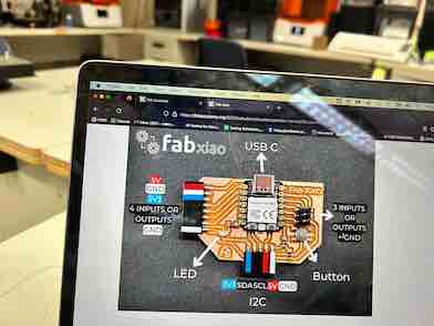
To prepare for week 8, I decided to solder theSeeeduino XIAO RP2040 now.
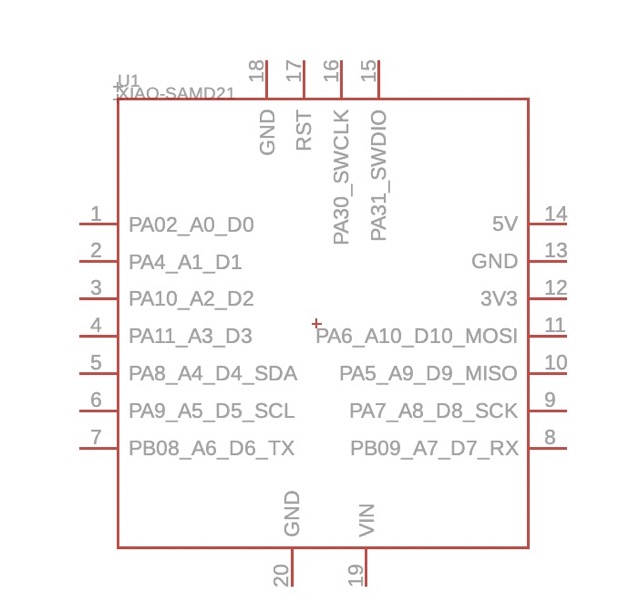
I first studied the pinouts as provided by Adrian Torres.
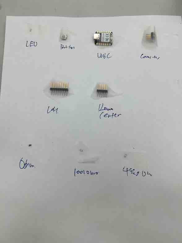
I gathered all my materials and put them on a single sheet of paper:
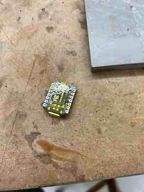
I covered the bottom of the Seeed with electric tape so that it doesn’t overheat when I am soldering it.
This is the completed soldering:
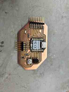
When I plugged the seeeduino into the computer via a USB cable, it worked!