PCB Design
EagleCAD
EagleCAD Tutorial
I followed this website and this website to learn how to use EagleCAD.
First I followed this linked tutorial for installing and setting up EagleCAD. I signed into this website and downloaded the free software (I believe I'll be able to link my Fusion360 educational license later).
I quickly stopped myself and realized that our lab provided a tutorial series that uses EagleCAD built into Fusion360. I first watched this tutorial to set up my software.
In the second tutorial in the series a library popup up out of nowhere and the tutorial expected us to have it installed. In the comment I found discussions of the same problem which pointed me to this link. I clicked Download. I then opened the project folder in Fusion 360 then clicked Upload and selected the downloaded FLBR file. I pressed Upload, and when it finished, I continued on with the tutorial.
This tutorial was very painful to complete, especially since I wasn't using a mouse. I found it very hard to accurately click on components so I could rearrange them, and trying to follow along with rearranging the schematic and doing it locally in Fusion was very annoying.
The video also mentioned the importance of a 0.1in grid but I had no idea where to check this, but I eventually realize at the top of the docuement it displays the grid size. Mine is already set and I won't be changing it anytime soon so I'm all set.
Also I never knew that CSV actually means Character Separated Values, not Comma Separation Values.
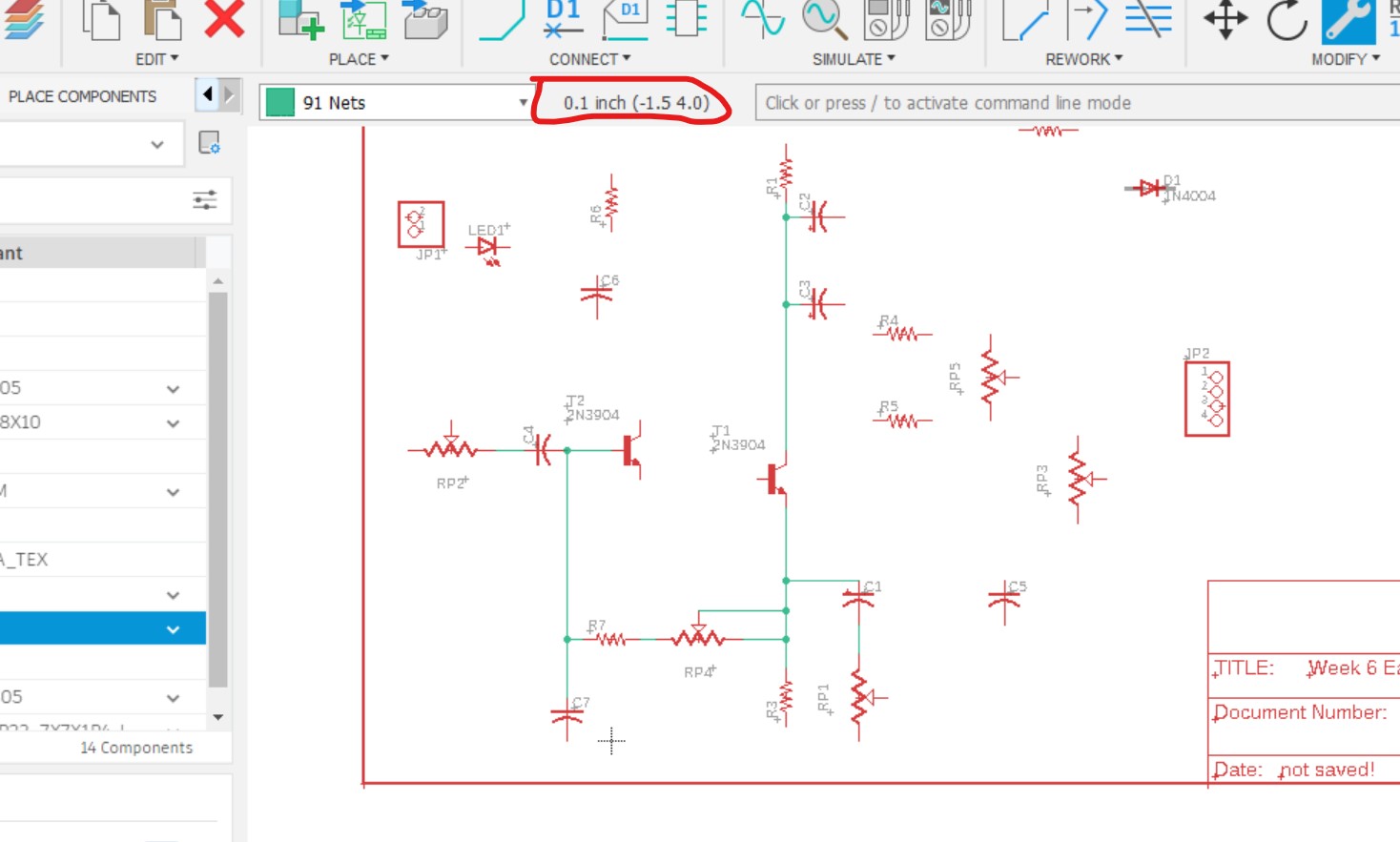
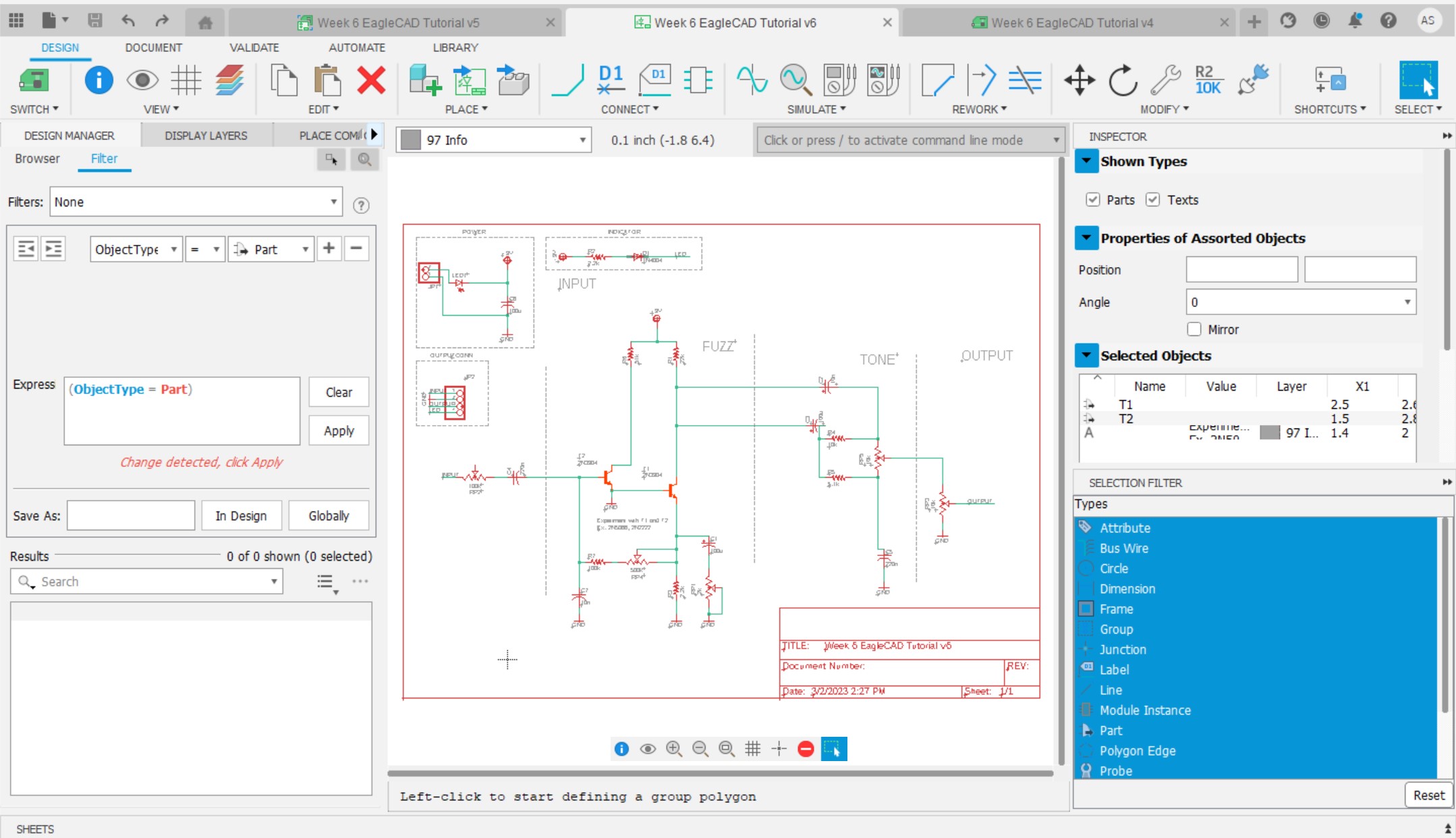
Here's my completed schematic from the tutorial.
I then followed the third tutorial
Instead of downloaded a case I just made a 30x40mm box with 20mm height, 1mm shell, 3mm offset construction plane from the bottom, 3mm fillet on all the inside edges, then projected the inside outline onto the sketch.
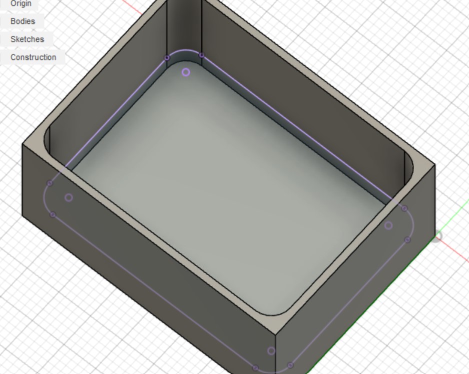
Then I made a -2mm offset of the projection and continued with the tutorial. In the tutorial I leanred difference between creating and independent and associative PCBs in EagleCAD.
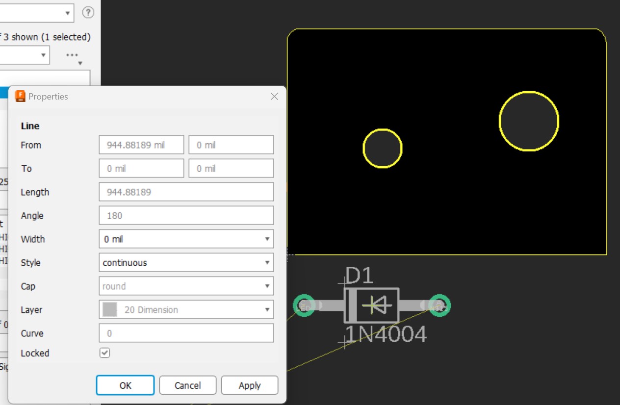
When learning about the fourth way to make a PCB, I couldn't delete the board outline in the 2d component placing menu. After struggling with this for a while, I right-clicked after selecting the entire board and pressed properties where I realized these layer-20 items were locked! So I unlocked them, hit Apply, then was able to delete a part. For some reason each time I did this it only deleted one line. So I just did it many times until all of the lines were defeated. I'm sure there's some way to unlock the whole layer but for now my solution is sufficient.
I also encountered a problem when trying to put the EIP workflow PCB to a 3D model.
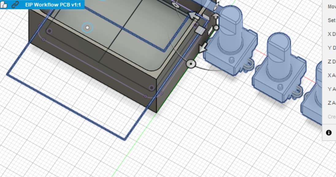
I realized I accientally did everything on layer 1, so I tried selecting them and changing the properties, but once again this only worked for one line at a time. So I just deleted all of them (which worked this time) and changed the layer at the top of the editing window to 20 and recreated the lines. This worked after a re-pushed the changed design to a 3d model.
As a started the fourth tutorial, for some reason my view in the 2D PCB editor was from the back of the board! I don't know how I did this, but after playing around for a while I realized I had to press Layer > Flip Board, and I went back to the other side.
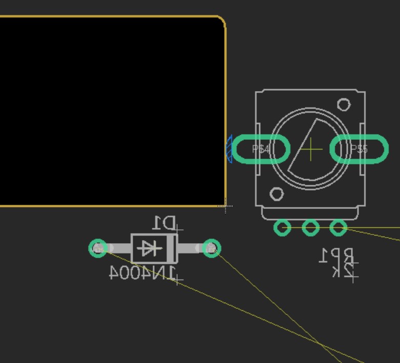
My board was too small to fit all the components in the fourth tutorial so I just modified it using the EIP workflow that the third tutorial described.
Eventually I just couldn't click or move anything, and I got the Windows error noise whenever I tried to right-click.
Finally I figured it out! I first read this forum which discussed changing the grid size, and I played around with this method of changing it but realized it's probably not the issue since I can't move things at all and my grid size was set to the default 50mm. I then read this post which suggested I didn't have all the layers turned on, so I played around with activating and deactivating different layers but none of this helped. Then, I scrolled down in that post and saw that I needed to simply click on the cross-hair in the component! I kept trying to click on the lines on the side of it but when I dragged it from the middle it worked! I later learned that this is also where I needed to right-click.
Also, middle-clicking on my touchpad while dragging a piece didn't flip it to the other side of the board but this post told me I could right-click on a piece (while not moving it so it doesn't rotate) and check the Mirrored box in the Properties dialogue to also flip it, and this worked!
A difference I noticed between KiCAD and EagleCAD is that KiCad, according to this website, is able to automatically place components in the layout/footprint editor, while this post indicates that EagleCAD is unable to do so.
I learned that it is very important to configure DRC tolerances to make sure the design can be manufactured.
Instead of following how the tutorial routed all of the pieces I watched this tutorial on how to use the autorouting tool in EagleCAD which worked perfectly!
When I tried running the DRC check I got four errors but realized I had simply placed some components too close to the edge of the board wtih my set tolerances.
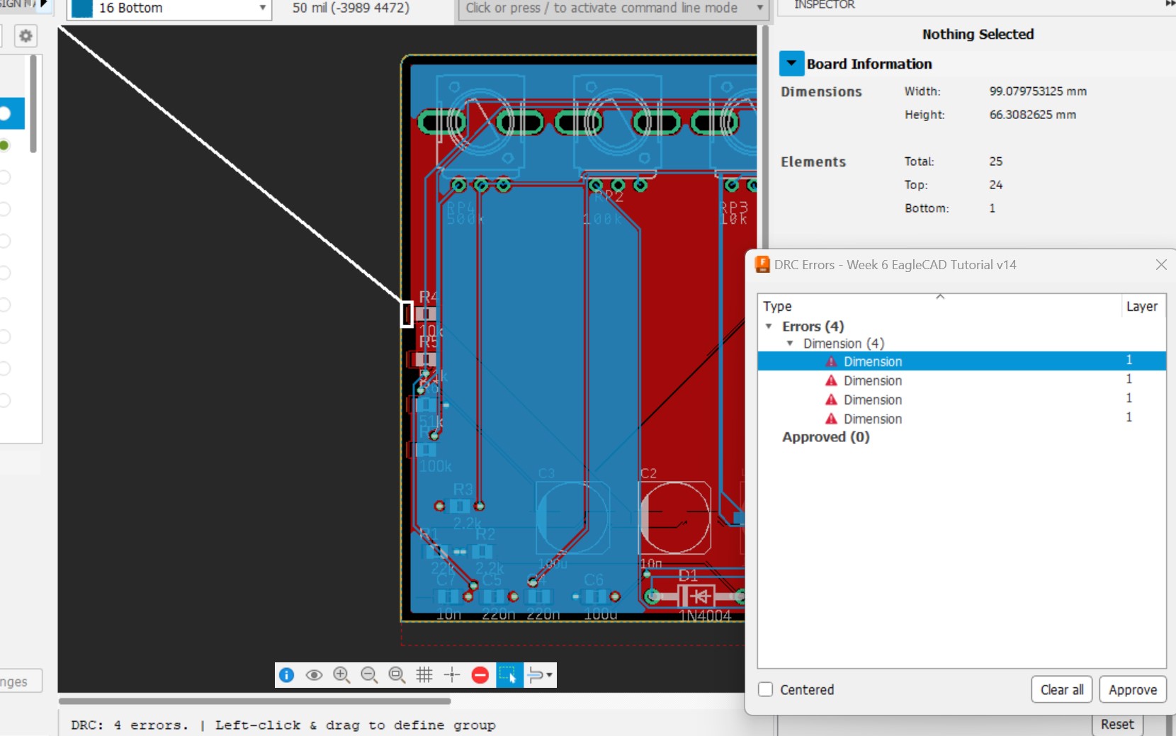
After moving the components closer into the board, the DRC had no errors!
I accidentaly placed the text on the bottom layer, so I right-clicked on the cross-hair, opened the Properties dialogue, and changed the layer to 21 tPlace.
I also wasn't completely sure why or whether it was necessary to activate polygon fills before pushing to the 3D model from the layout editor, but I just followed along with the tutorial's guidance for now.
Finally I watched the final tutorial about preparing a design for manufacturing.
Before opening the CAM processor, a popup window reminded me that only the most recent saved version will be displayed, so I made sure to save the most recent changes before entering this window.
The video also mentioned that it's extremely important to check exported files with programs such as GERBER viewers before sending off files to a manufacturer for production. For the time being, though, I didn't follow along with the last part of the tutorial that uses a GERBER viewer to check that the files are accurate.
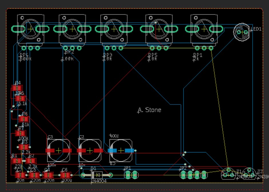
Here is my final routed board from the tutorial.
Designing A PCB
Fixing Fusion 360 CAD
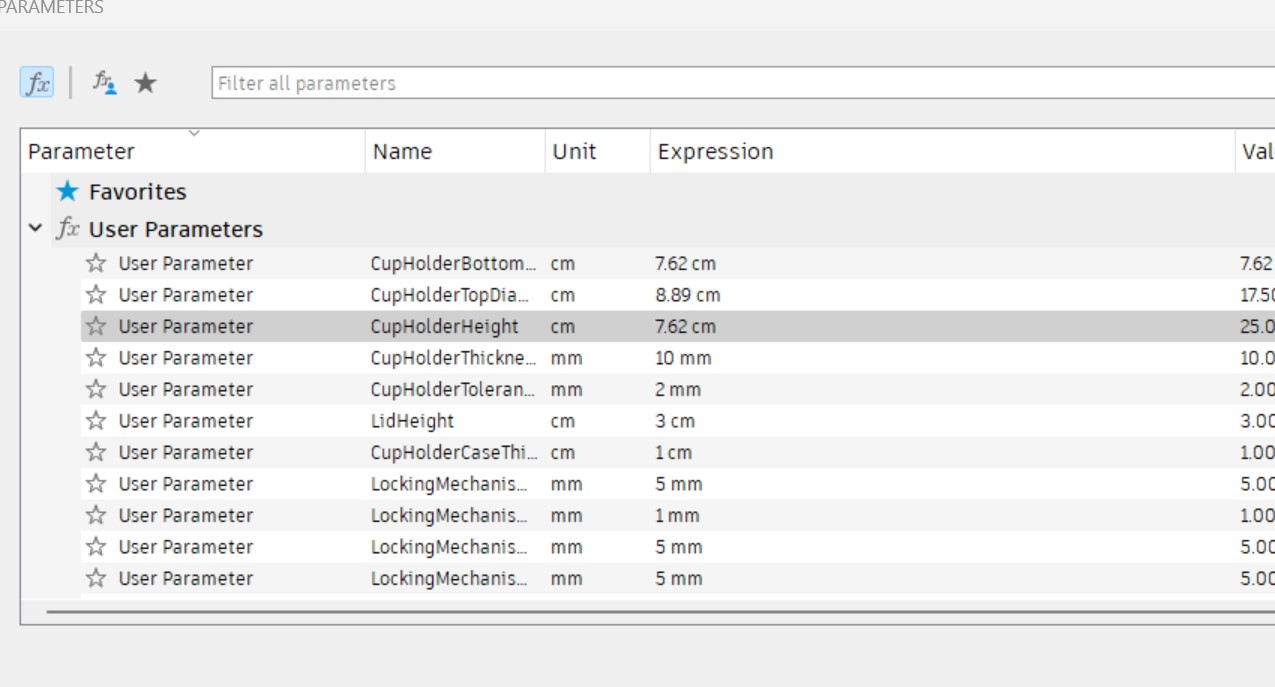
Before making my PCB, I wanted to make sure that I had finalized dimensions for my 3D model from CAD Week so I found this website which explained standard cupholder dimensions. I decided to make the bottom diameter 3in, the top diameter 3.5in, and the height 3in. entered these values in the User Parameters I had created in Fusion 360.
Yet I recieved several errors and the design looked wrong.
I realized that the problem possibly occured in this sketch because I may have not made it totally parametric.
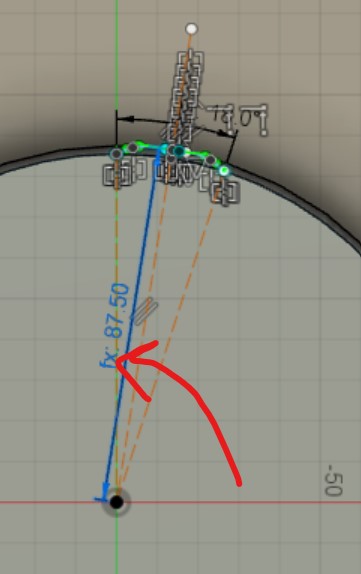
To see whether this was the issue I undid the parameters then opened the sketch. I then set a parameter for the distance between the splin and the center to be CupHolderTopDiameter / 2.
Then the circular patter of this extrusion turned red in the timeline, so I opened it and it looked OK so I exited the dialogue and suddenly there weren't anymore errors.
Now I changed the parameters back and some of the fillets were red again. I changed the parameters to what I originally had and examined what the fillets dealt with.
For some reason upon doing this I went back to the smaller parameters, and it fixed itself again!
I realized the problem was that a subtractive extrusion I made in the bottom of the lid was not parametered, so when I made the lid smaller, it deleted everything on the bottom of the lid, leaving nowhere to do the fillet. I simply dimensioned the circle to be 15mm from the outside of the circle and it worked!
I realize that the model isn't right in the cup holder now that the height is smaller, but this is only an aesthetic difference in Fusion 360 and not something worth dealing with at the moment.
I created a new save called parameters-fixed and began to work on creating the sketch for the PCB.
Sketching The PCB
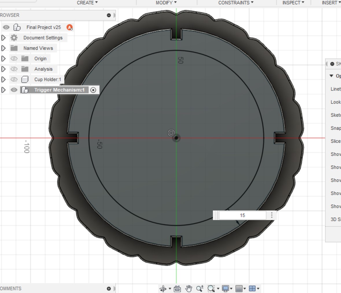
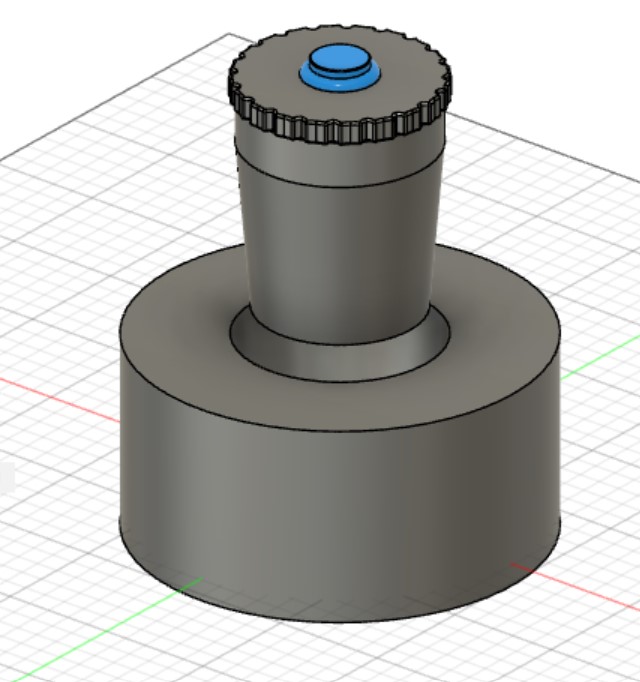
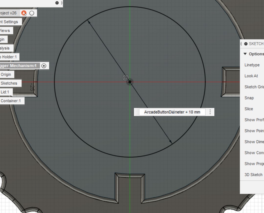
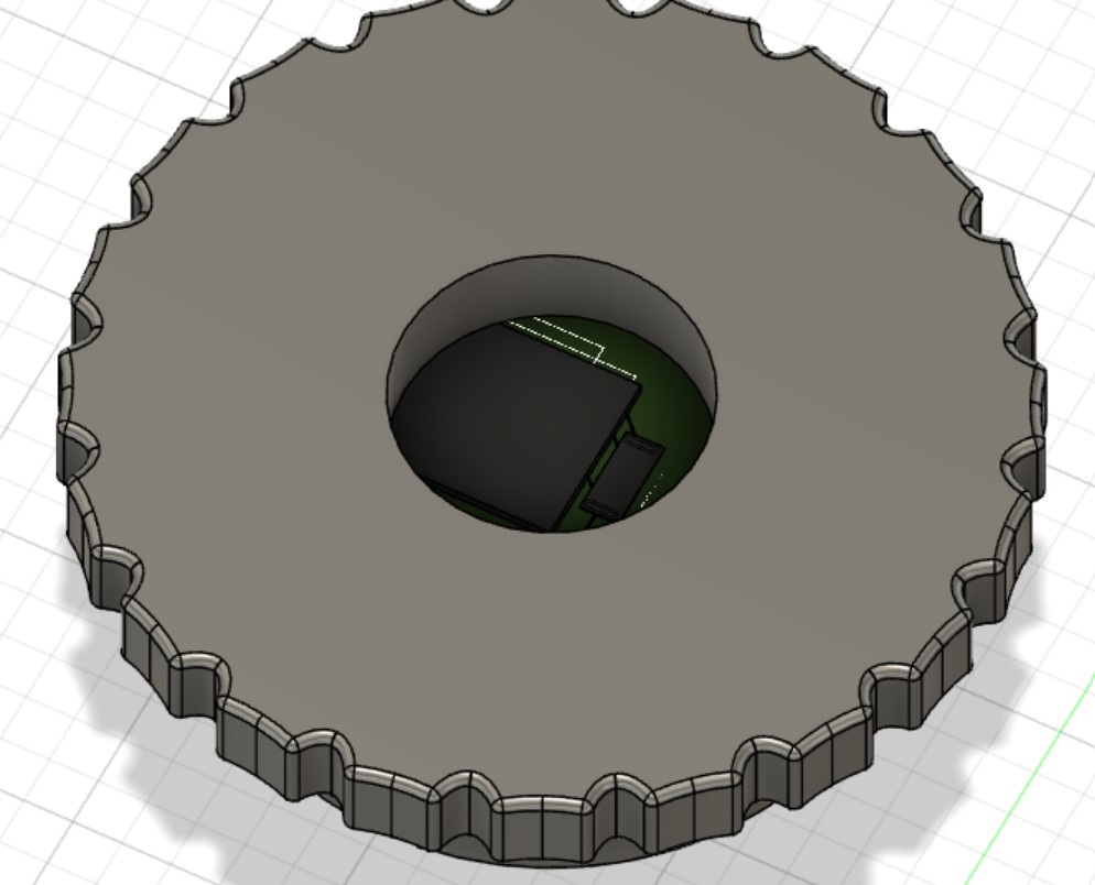
To make it so that the side of the PCB would never change, I changed the dimension of the subtractive extrusion once again to be the nominal diameter of the button + 10mm so that the PCB would always be a 40mm diameter circle. The first time I changed this I had an error regenerating the rest of the design but realized that I simply should have clicked Revert Position in the dialogue box that appeared when editing the sketch. After redoing this step, it worked!
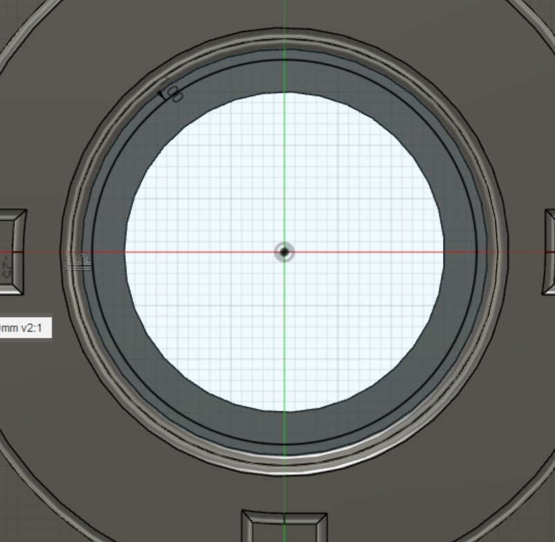
I then created an offset of 1mm from the circle and used that sketch to create a PCB!
I renamed the sketch pcb-sketch and made a new save of the same name.
I made a new folder in my Final Project folder called PCB and went to File > New Electronics Design. I pressed Create > New Schematic then downloaded this file by right-clicking on the Raw button and pressing Save link as.... I then pressed s in fusion to open the shortcut box and ran the Open Library Manager command. I then pressed the Import Library button in the top-right and selected the downloaded LBR file.
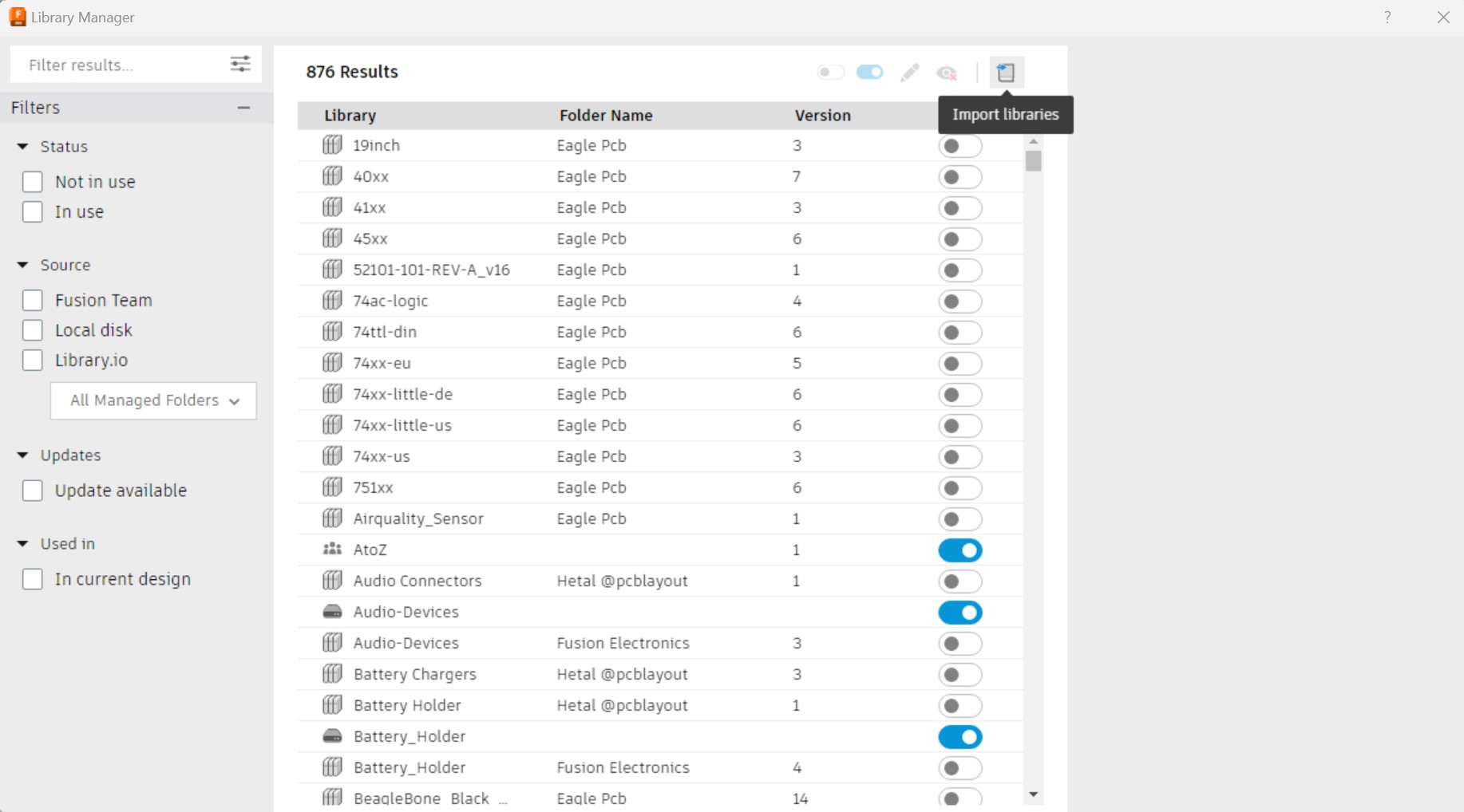
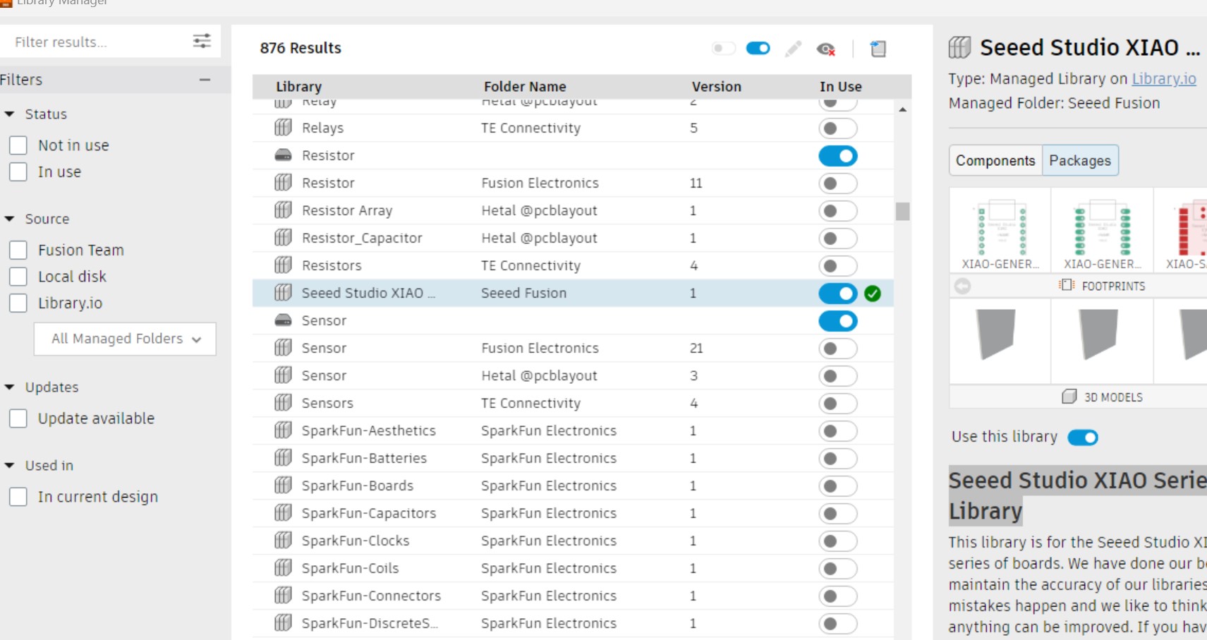
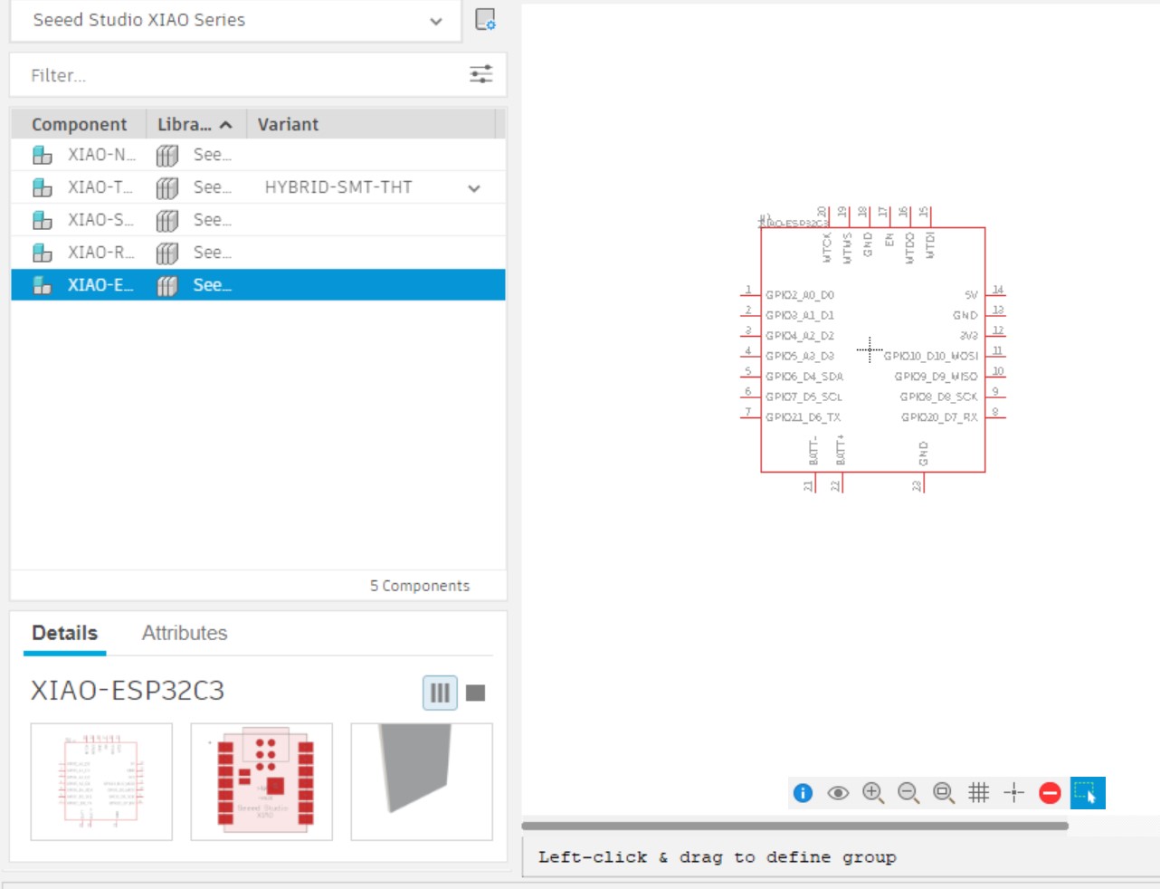
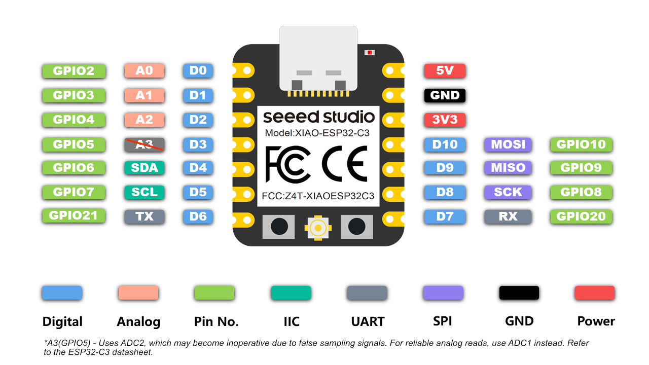
I opened the Library Manager and turned on the Seed XIAO component library because this website says that it has Wifi and Bluetooth functionality for wireless communication.
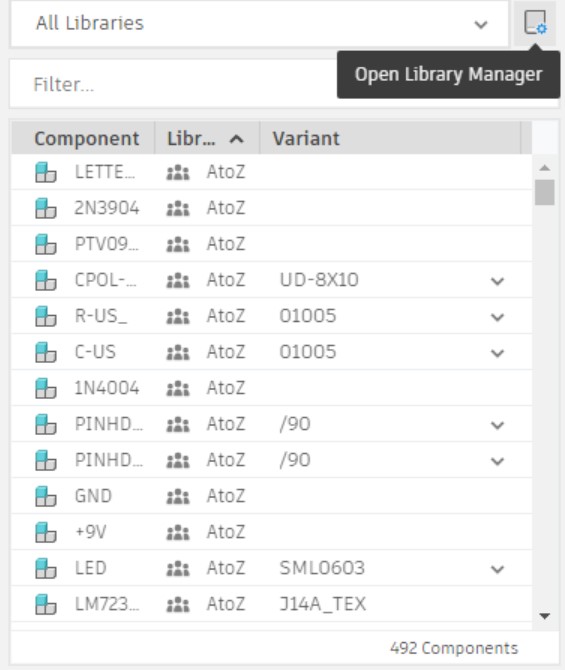
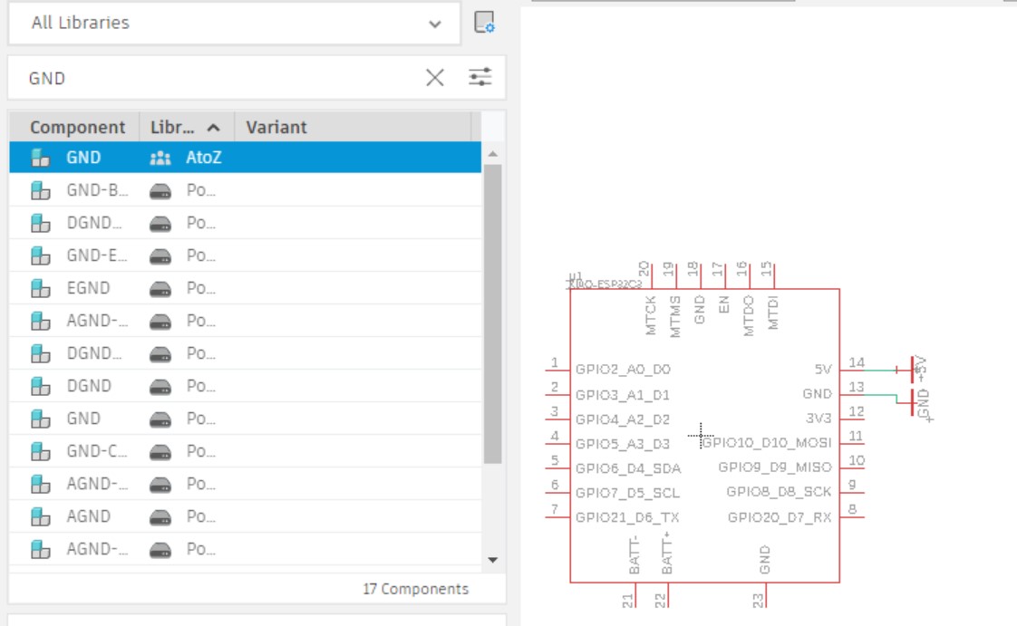
I then brought one of the ESP32-C3 components into my schematic.
I then dragged in the +5V and GND components and connected them to the power and ground of the microcontroller.
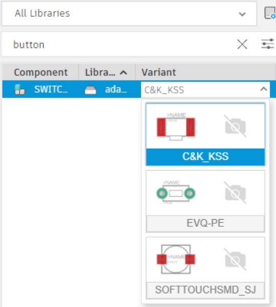
I then looked back at the link to the button model I used during CAD Week. Searching on DigiKey I found this 30mm Red Arcade Button.
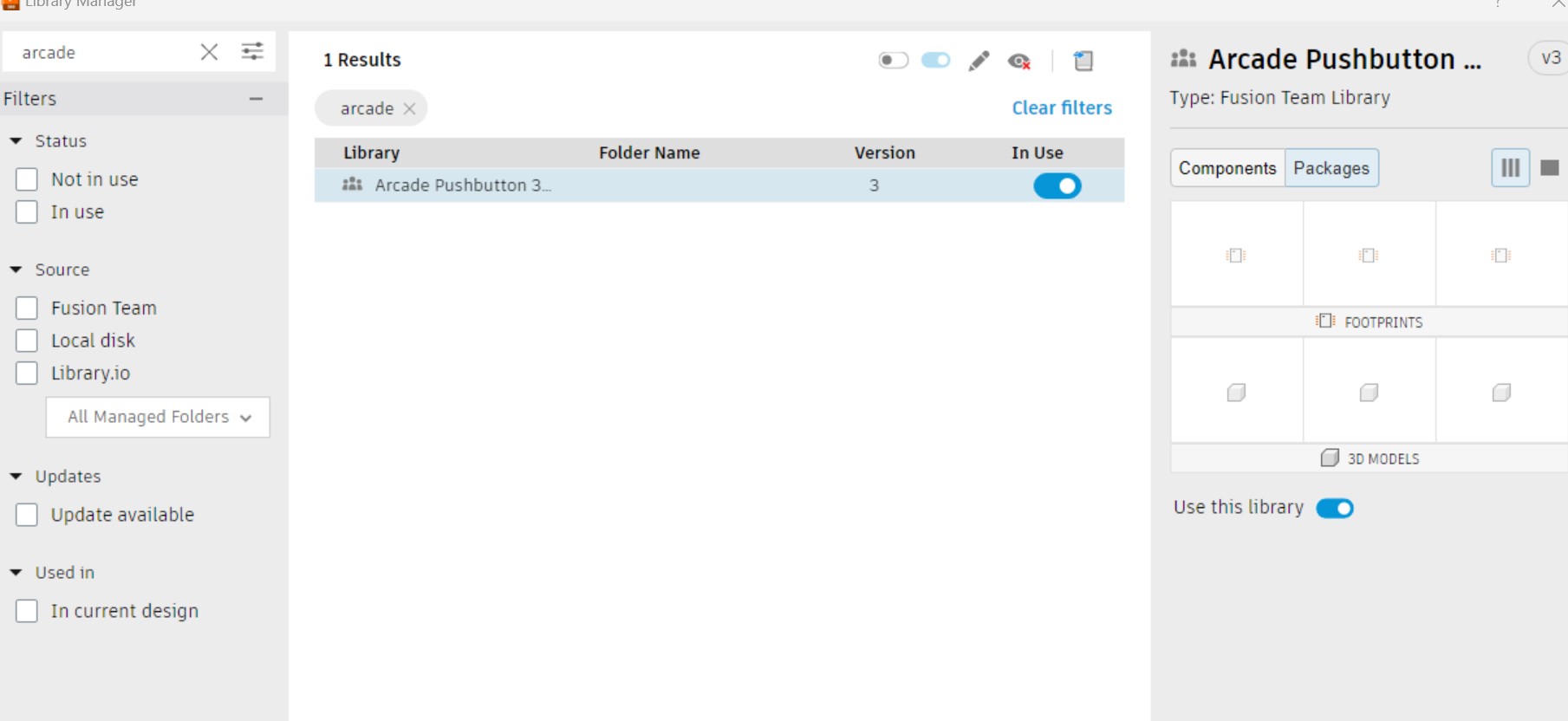
To try to get the EagleCAD model of this part, I downloaded this Adafruit EagleCAD Library and added the LBR file through the same process as before. Yet when I looked for the components none of the footprints looked correct for the pushbutton.
I spent a very long time trying to find the correct library, and after discussing with Dr. Fagan, decided to create my own.
Creating a Custom EagleCAD Component
I followed this tutorial to make my own component in EagleCAD.
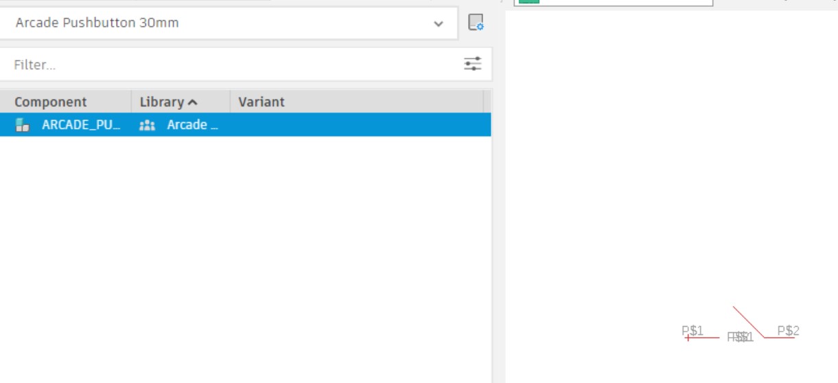
I created a library called Arcade Pushbutton 30mm and opened the fab.lbr library that I previously downloaded to get the schematic symbol. I couldn't find the desired symbol in the fab.lbr library so I opened the buttons.lbr library. I also couldn't find it there, but I did find it as the SWITCH_PUSHBUTTON component in the adafruit.lbr library.
I found the article very hard to follow along with so I found this video tutorial instead. I used the technical drawing on the datasheet linked on the DigiKey page to get the dimensions. I also measured some things not mentioned in the technical drawing.
For the through-hole pads, I measured the dimensions of the pins on the parts.
Then, as per this post, made the dimensions 10% larger than my measurements.
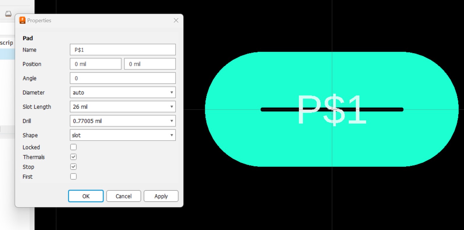
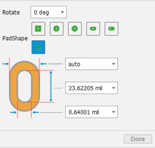
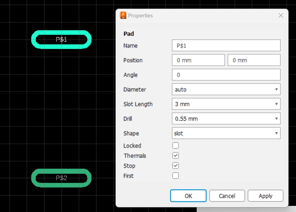
The distance between the pins I got was 7.5mm, so accounting for the width of the pins being 0.5mm, I would make the pads 8mm apart. The width of each pin was 2.7mm roughly so I made the width of the pdas 3mm (I updated the measurements from the previous picture).
Finally I realized I was accidentally working in mil not mm. I changed the grid units to mm and grid-size to 1mm and also updated the pad measurements.
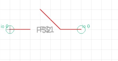
I drew lines for the symbol and put them on the 51 tDocu layer one-by-one. I made a text item of the name and put it on the 25 tNames layer.
I then added a symbol and made a very simple design.
I went back to my schematic and saw my library was activated!
I realized that there was no component avaiable! So I went back to the library, added a component, used the Add command to add the symbol, clicked New and selected the package, clicked Connect and connected pin 1 to pad 1 and pin 2 to pad 2, and saved the library. Then I was able to import it into my design!
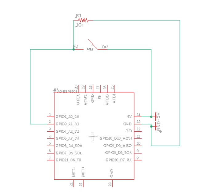
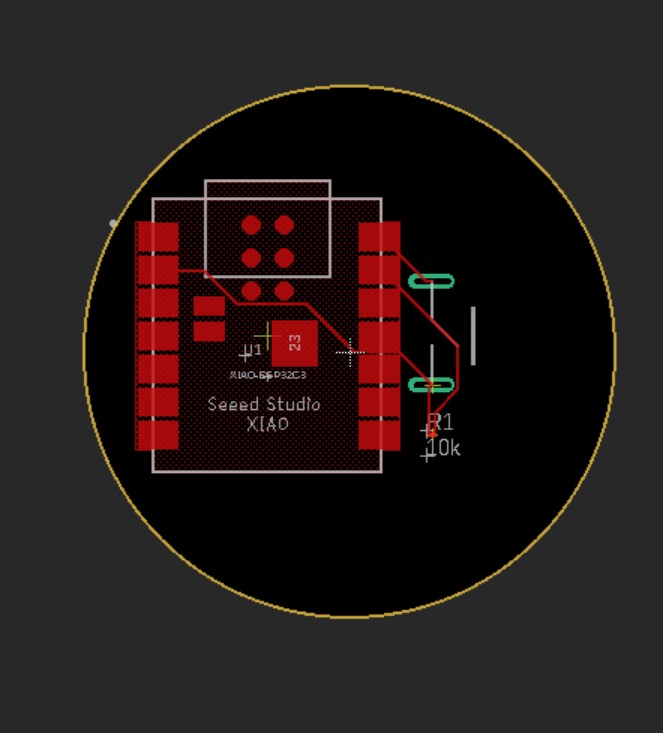
I used this pinout sheet to wire my schematic.
I then pressed Switch to PCB Document and deleted the board shape. I pressed Board Shape > Outline Circle and made a temporary circle for the outline of my board.
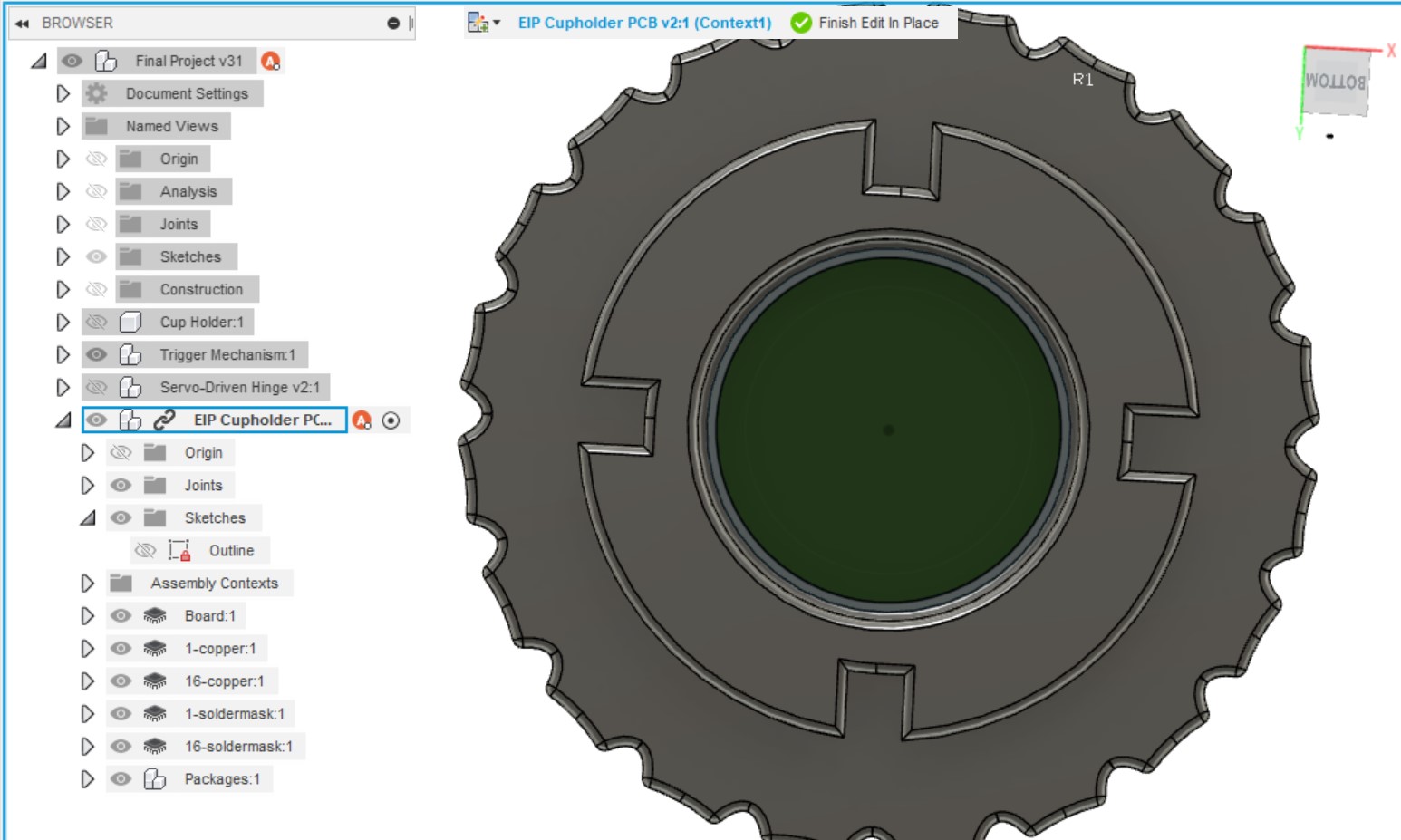
There was barely enough space for the PCB, so I increased the size of the circle with an offset of 10mm to 15mm. After pushing everything, laying out the components, and auto-routing, I oriented the PCB correctly in the project design and everything worked!
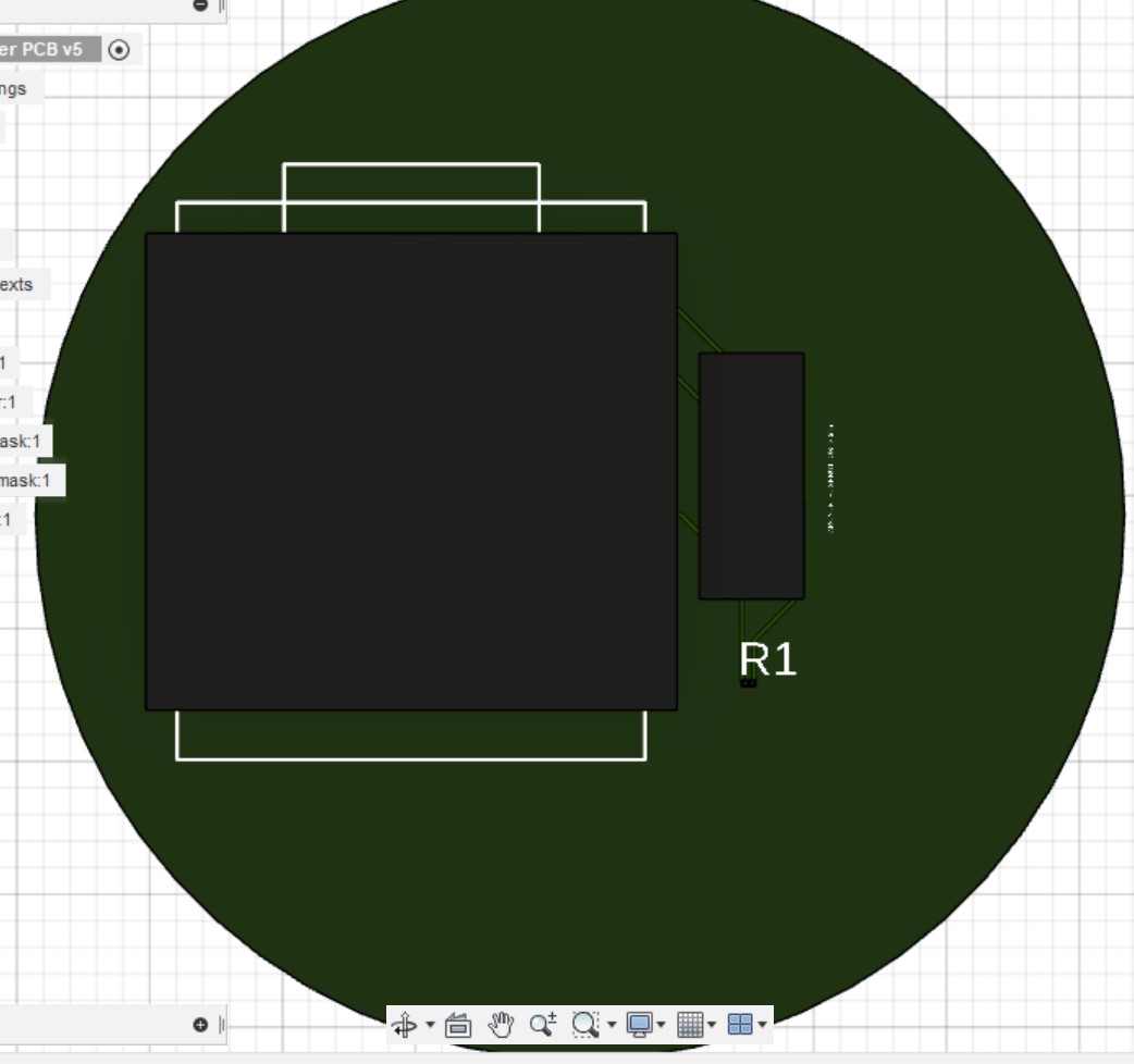
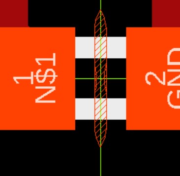
When I ran the DRC I recieved an error wabout the clearance on the resistor, but since I'm not manufacturing this week, I decided to leave it since I can always swap it out for a larger resistor in the future.
KiCAD
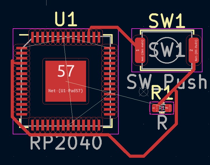
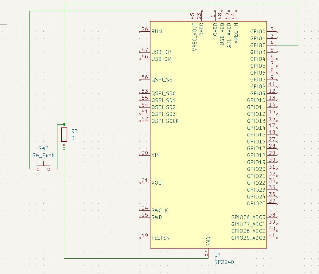
I made a new KiCAD project and opened the Schematic Editor. I added the Resistor and rp2040 components (I didn't want to deal with importing the XIAO board again considering I already created the EagleCAD model). I then finished the schematic relatively easily. The only problem was that I sometimes had to hold down Ctrl to be able to connect a wire to a pad because the grid size was fairly large.
I then opened the PCB Editor. As per this tutorial I tried exporting a Netlist from the schematic then importing it into the layout, but I recieved errors about a lack of footprints when I tried this. So I right-clicked on the resistor and pushbutton individually, pressed Edit Footprint..., then somewhat arbitrarily chose a footprint for each one. This time when I exported then imported the netlist, it worked perfectly! I arranged the components and I was finished!
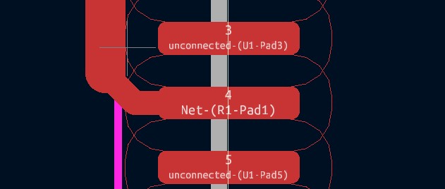
I couldn't route to the pads on the rp2040 chip as they were too close together for my route width. I tried changing many different settings in the Board Setup menu, but nothing seemed to help. I even tried adding a custom Track Width of 0.15mm in the Pre-defined Sizes menu, but this didn't help. It didn't appear as if the width of the route was actually changing.
I decided to try a different approach and make the route as close as possible to the pin then edit the properties of the last segment of the route to make it thinner then stretch it to the pin. This worked!
I also think I may have not connected to the correct power source, but for the time being what I have is acceptable for understanding the fundamentals of KiCAD.