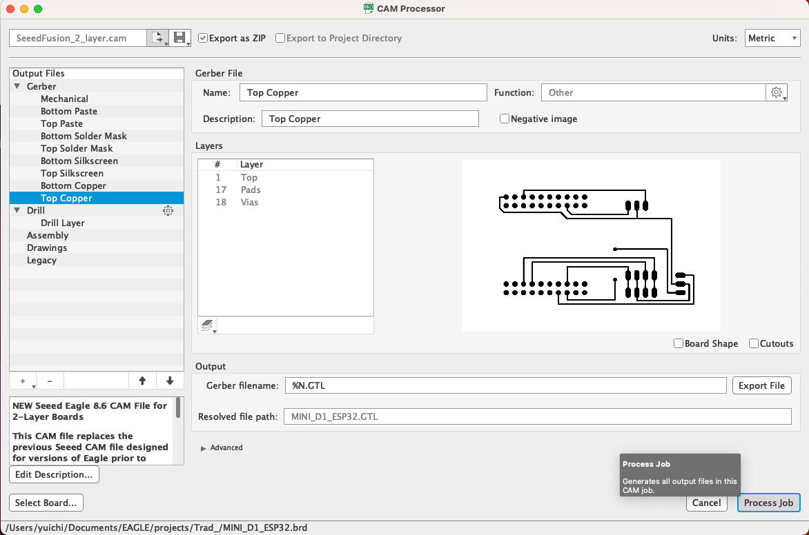
PCB sending out from Eagle to board house
Ref. Export Gerber file from Eagle_JP
Ref. seeed FusionPCB blog 基板製造の仕様_JP
Board house
Seeed Fusion PCB
Eagle
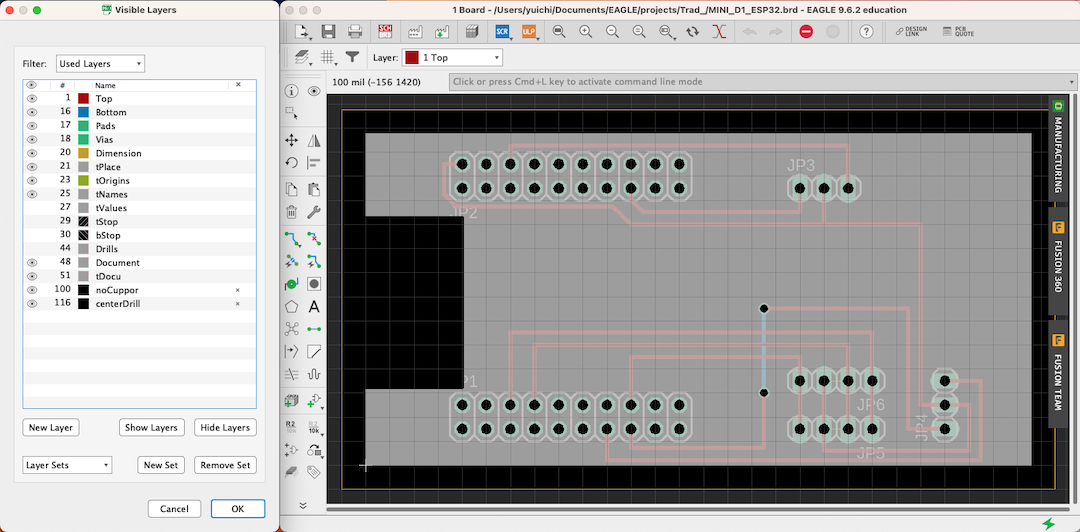
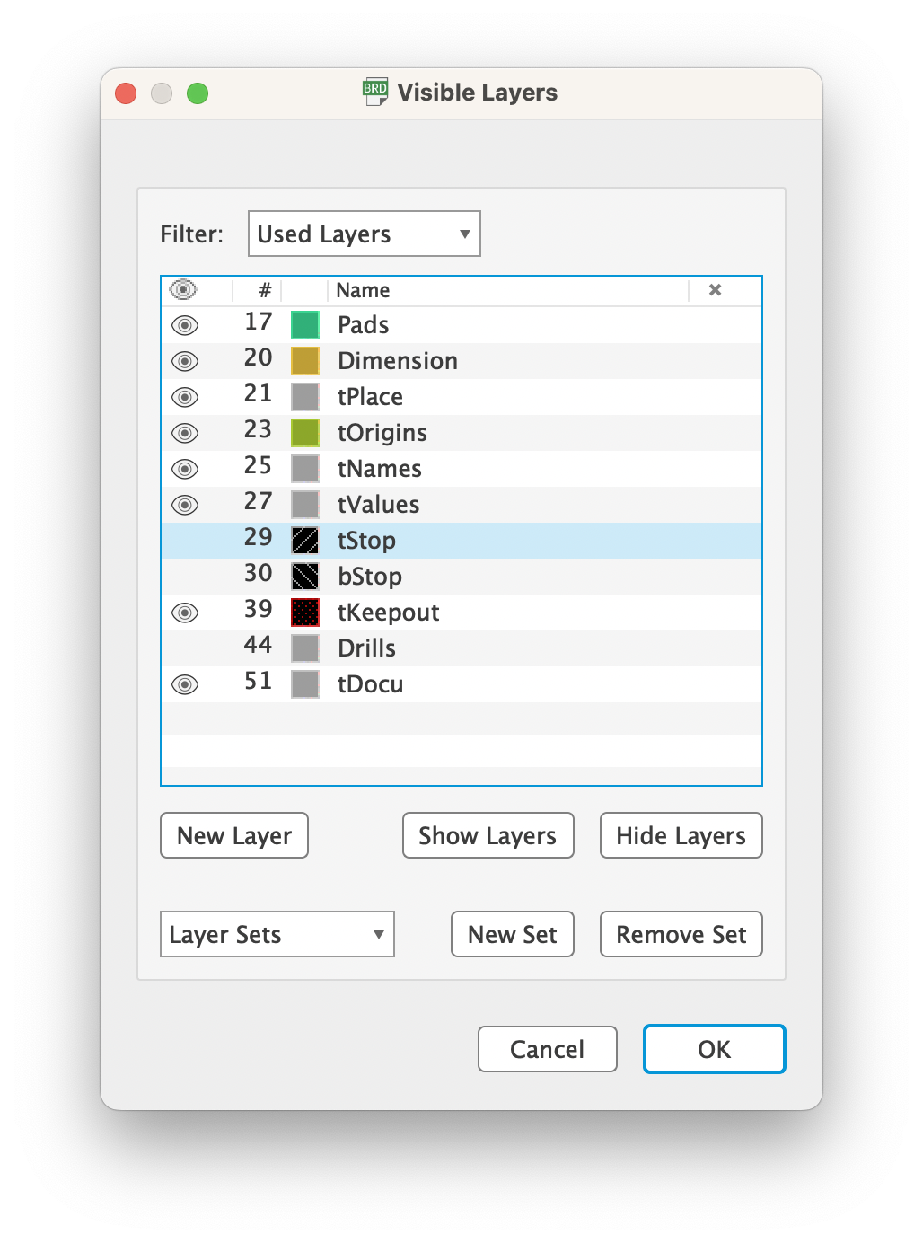
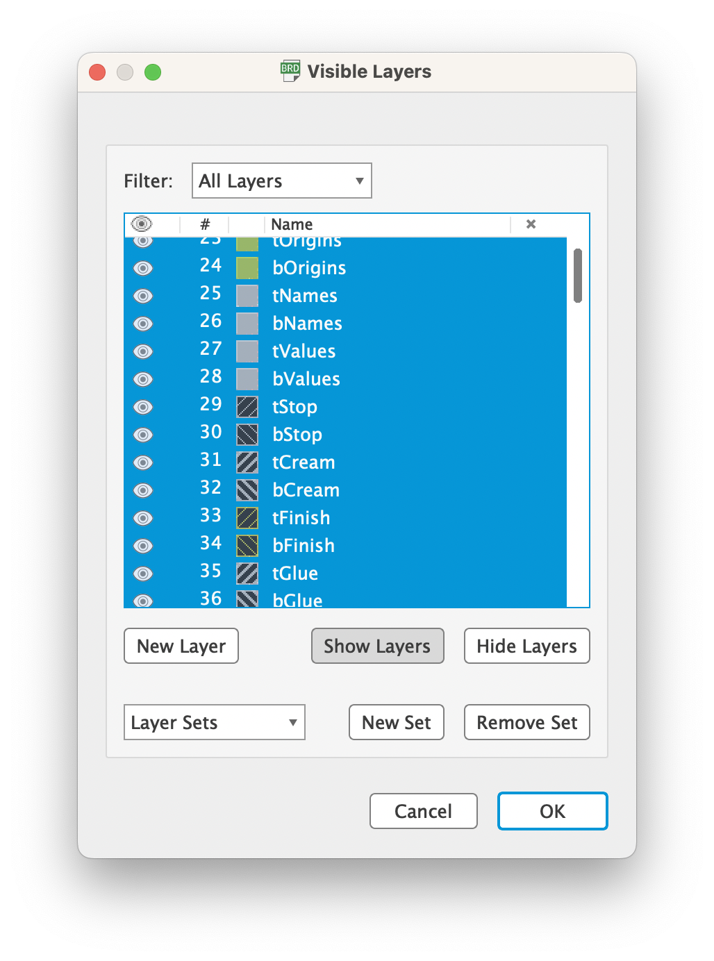
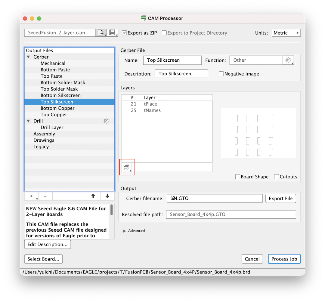
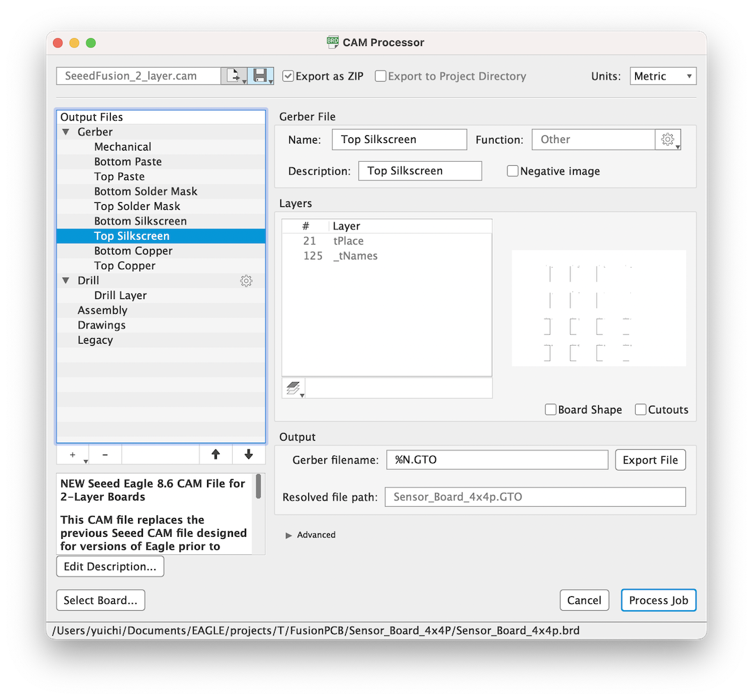
Relation Eagle layers and Gerber file
| Eagle Layers | Gerber and drill file | Single side PCB milling | |
|---|---|---|---|
| 1 Top 17 Pad 18 Vias |
Top Copper (.GTL) | 銅箔パターン(おもて面) | 1 Top 17 Pad 18 Vias |
| 16 Bottom 17 Pads 18 Vias |
Bottom copper (.GBL) | 銅箔パターン(裏面) | - |
| 21 tPlace 25 tNames |
Top Silkscreen (.GTO) | シルク印刷(おもて面) | - |
| 22 bPlace 26 bNames |
Bottom Silkscreen (.GBO) | シルク印刷(裏面) | - |
| 29 tStop | Top Soldermask (.GTS) | ソルダレジスト(おもて面) | - |
| 30 bStop | Bottom Soldermask (.GBS) | ソルダレジスト(裏面) | - |
| 20 Dimension 46 Milling |
Mechanical (.GML) | Board Outline 基板外形 |
 48 Document |
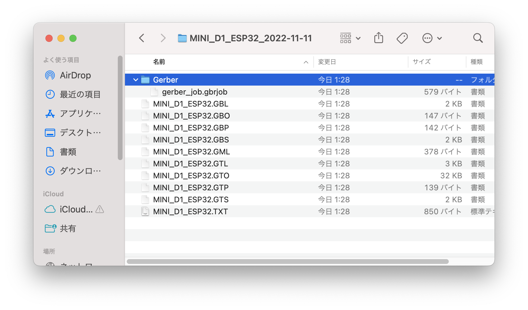
| Vias PTH Holes |
Drill Layer (.TXT) | ドリル | 116 centerDrill |
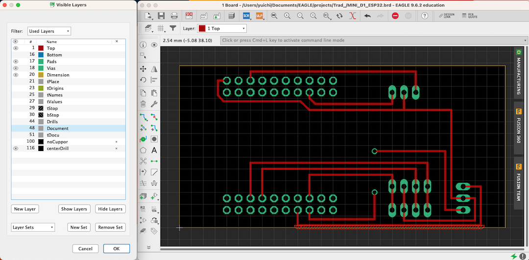
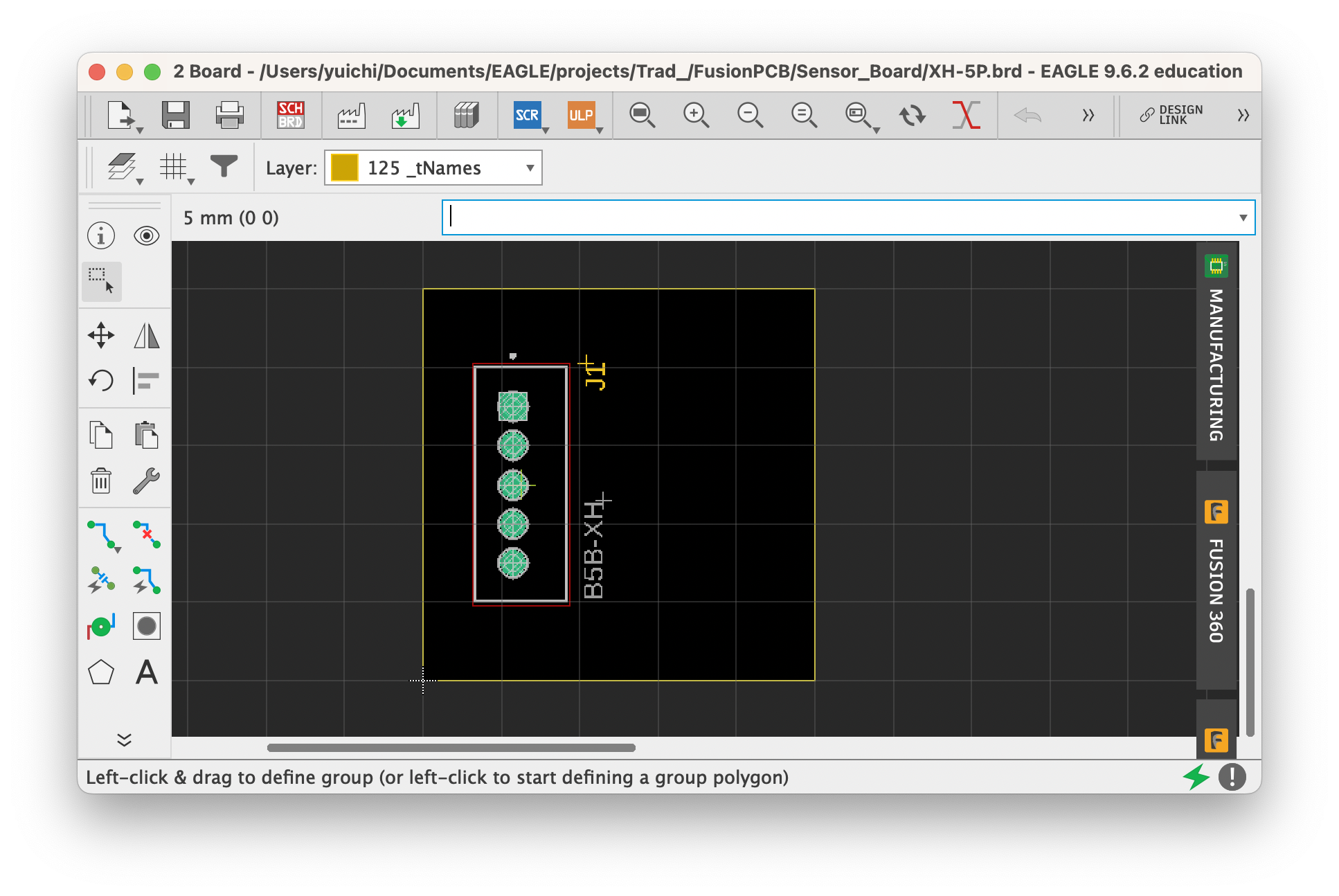
Board Outline
Attention
For PCB milling with mods, 48 Document is used as board outline and 20 Dimension is always larger than board size to make the outline milling path.
But for Gerber file, 20 Dimension will be board outline.
Move Dimension(yellow lines) to the board size
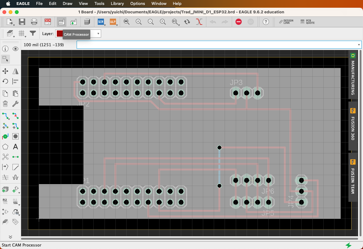
Steps
System Examples -> Third Party -> Seeed Fusion -> SeeedFusion_2_layer.cam
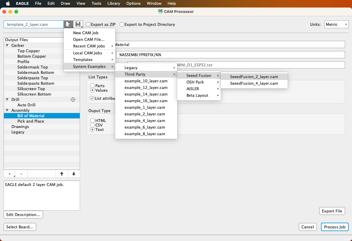
Saved as .zip file
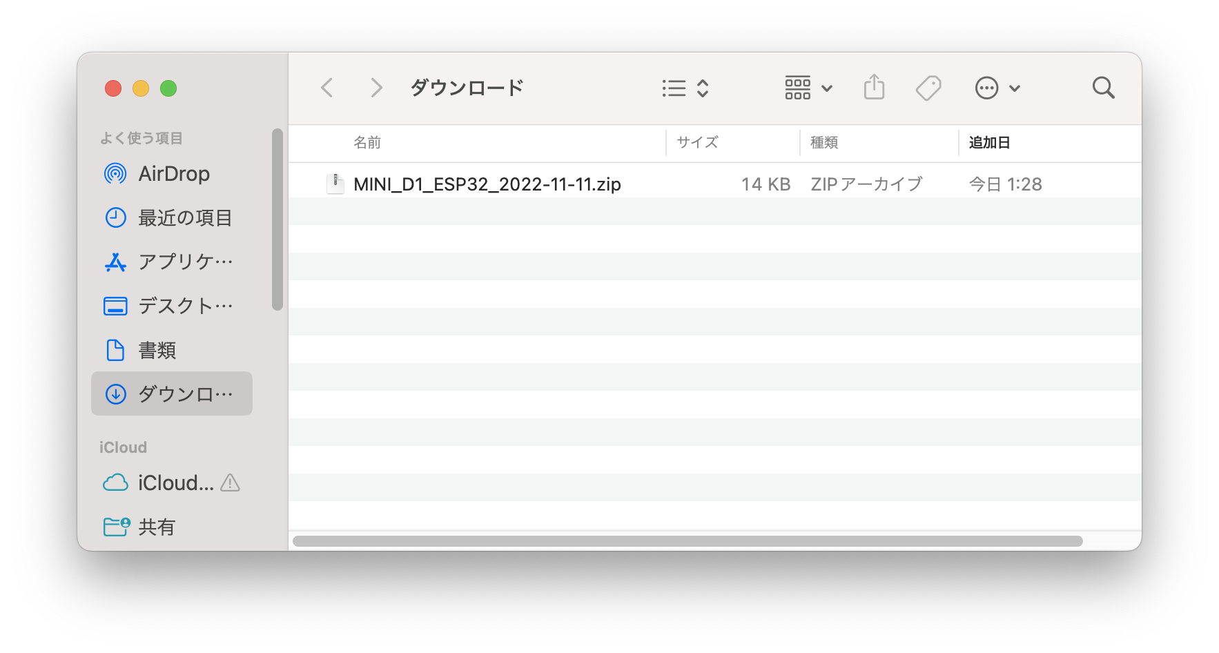
Note
No need to unzip
If unzip the zip file, these are included
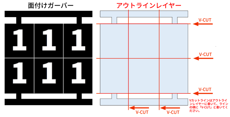
Panelize and V-cut (面付けとV-cut)
Ref . V-cut_JP
Why?
The manufacturing cost per board can be reduced by manufacturing multiple boards as a single board by laying them together.
If you specify V-Cut between the boards, you can divide it with your own hands.

面付けして複数の基板をまとめて1枚として製造すれば、基板1枚あたりの製造コストを下げることができます。
基板間をV-Cut指定しておけば、自分の手でパキパキ分割することができます。
Basic rule
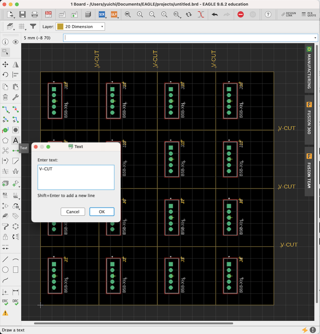
- Draw V-cut line on 20_Dimension layer in Eagle
- Impossible to V-cut on Round board shape. V-cut line should be straight from the edge of board to the other side of the edge
- Add mark “V-CUT” on 20_Dimension layer as below
4.Distance between V-cut line and Cupper line shoud be more than 0.4mm
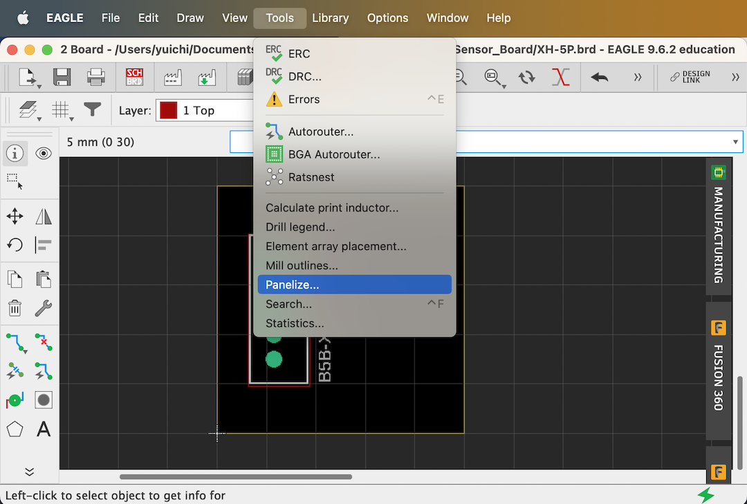
How to do
Ref. Panelize and V-cut in Eagle_JP
Tool -> Panelize… -> Execute
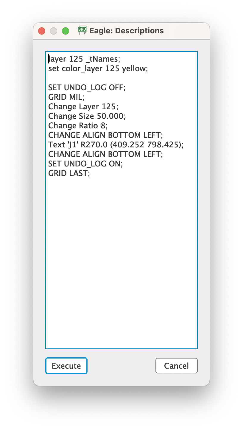
Note
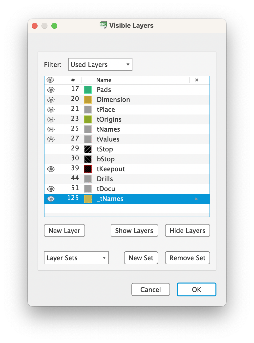
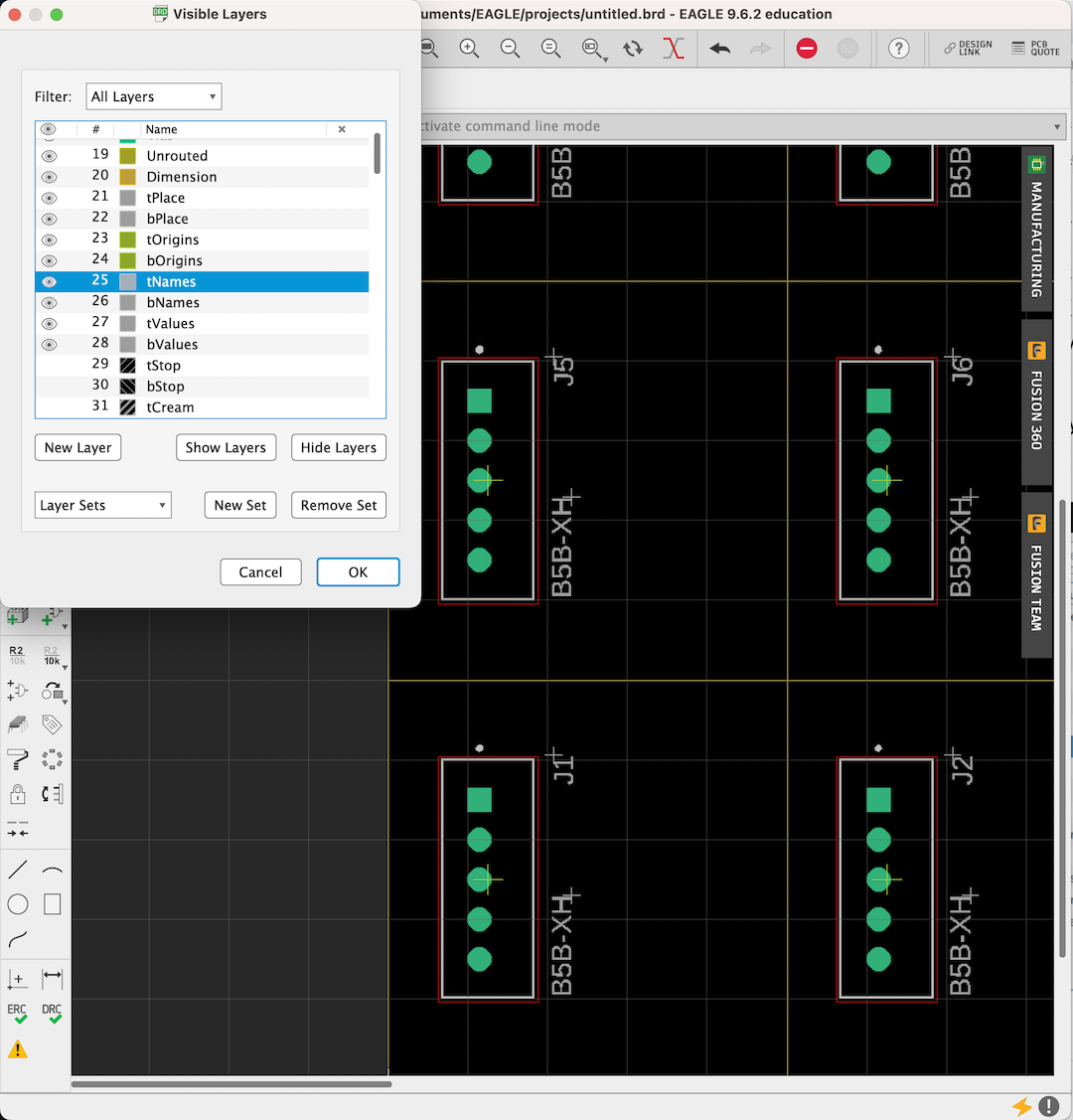
Layers will be Copied
- 25 tNames -> 125_tNames
- 26 bNames -> 126_bNames
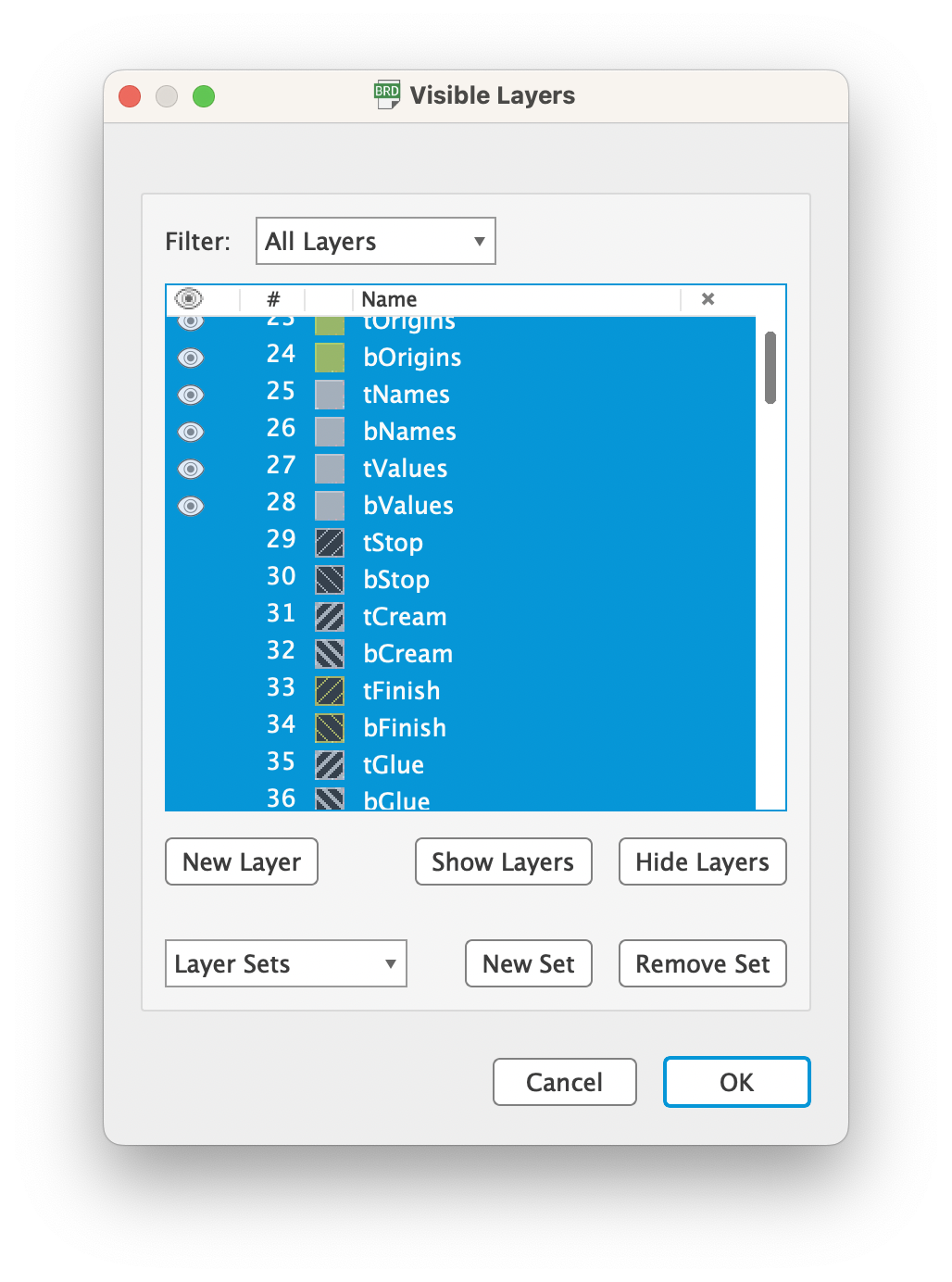
Show all laysers

- Move mouse pointer to (0,0)
- Ctrl + A
- Ctrl + C
- Ctrl + W -> Save -> No
Open new board
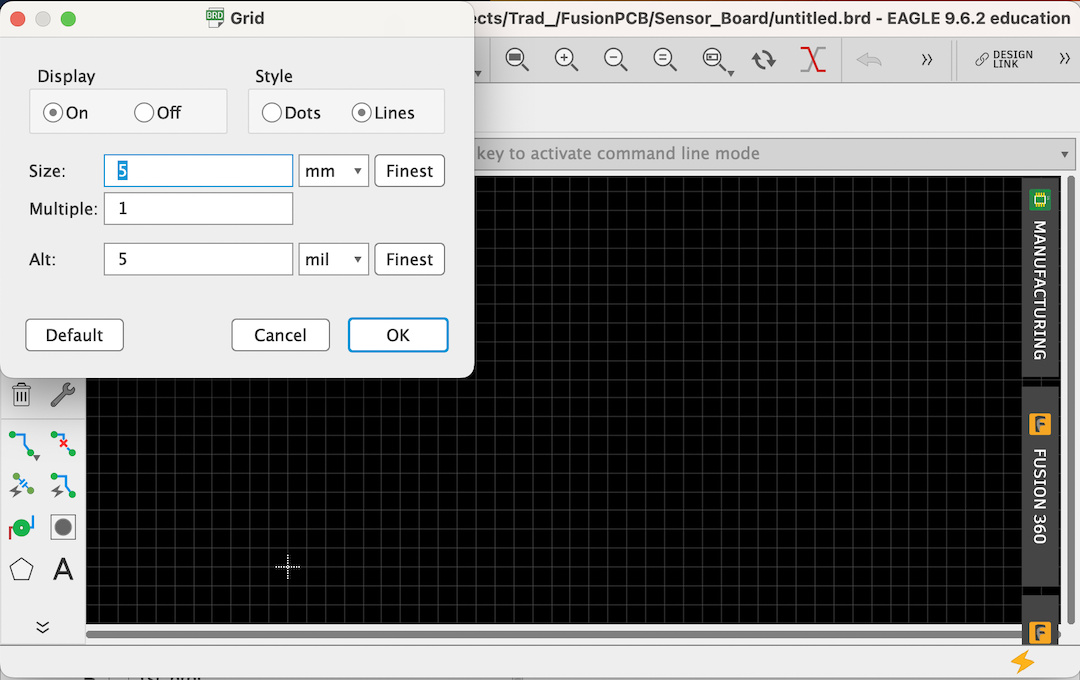
Set grid as same as the original board
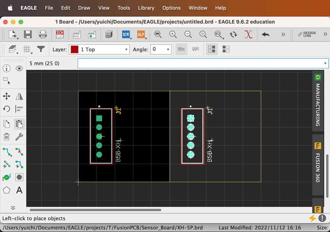
Paste (Ctrl + V ) at (0,0)
Paste (Ctrl + V ) just next to the previous one
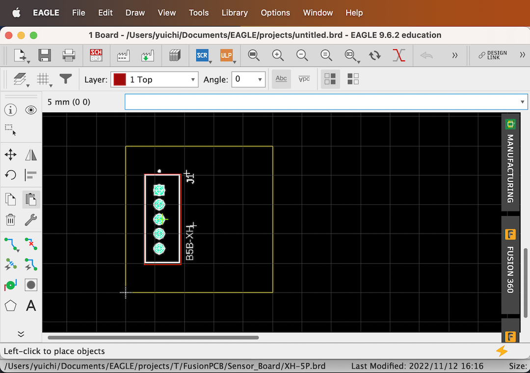
Two J1s exist in one board, not continuous numbers
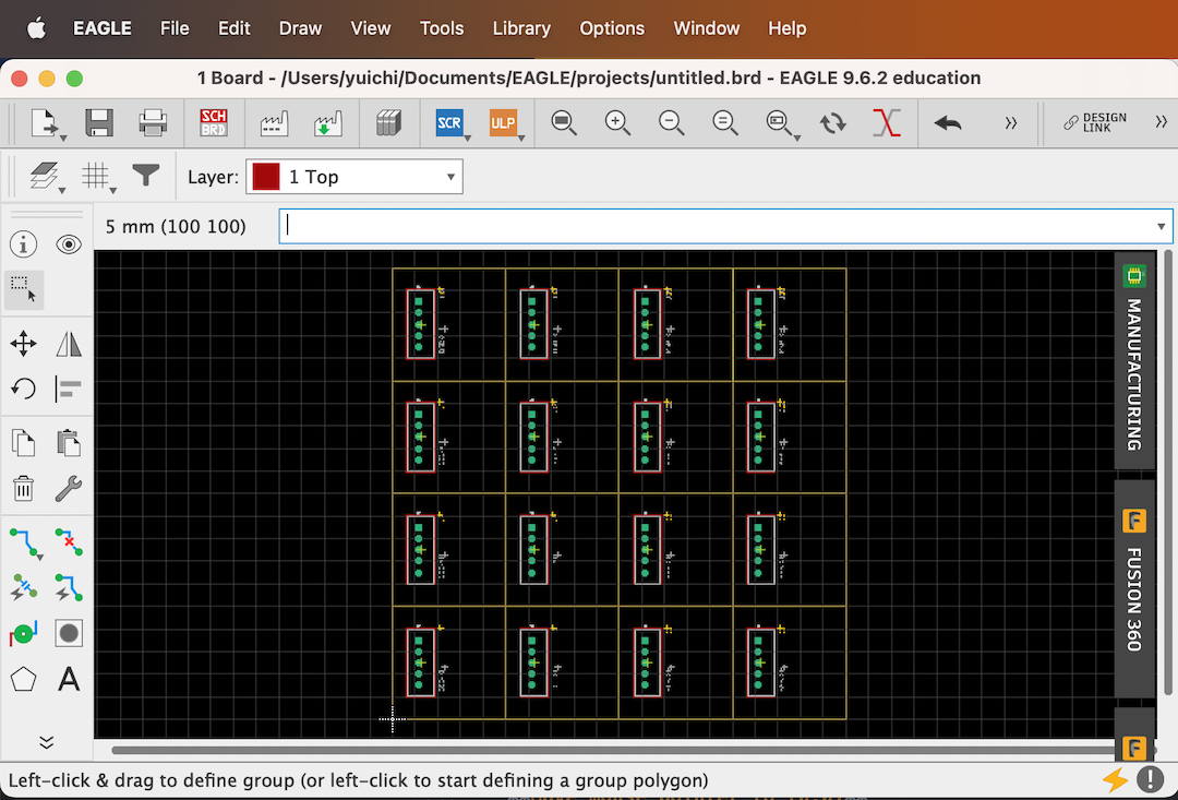
Paste (Ctrl + V ) until 100 x 100 mm size as minimize the cost
Redraw all Dimension line with Line Width 0
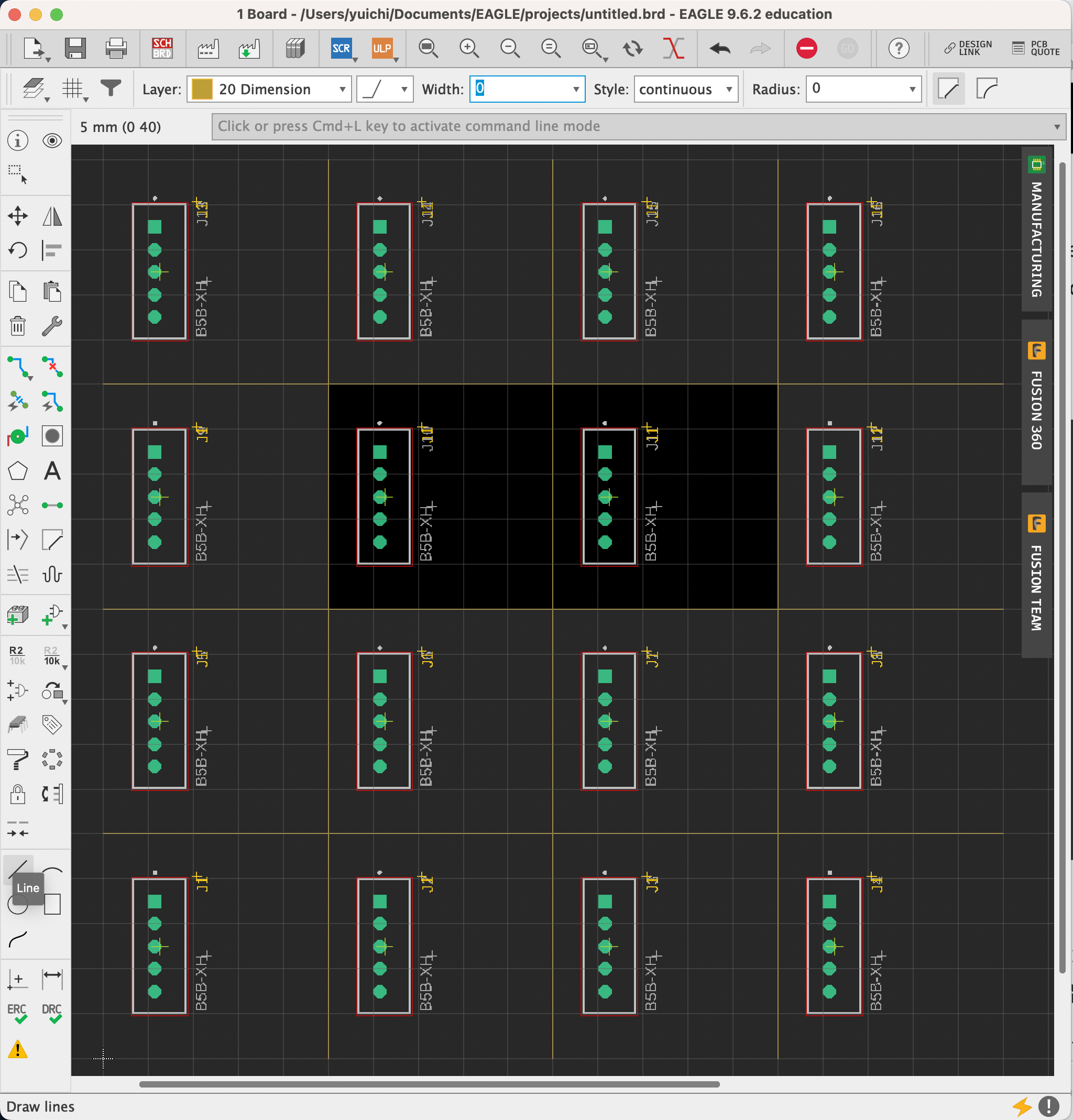
Add Text V-CUT on the same layer (20 Dimension)
Note
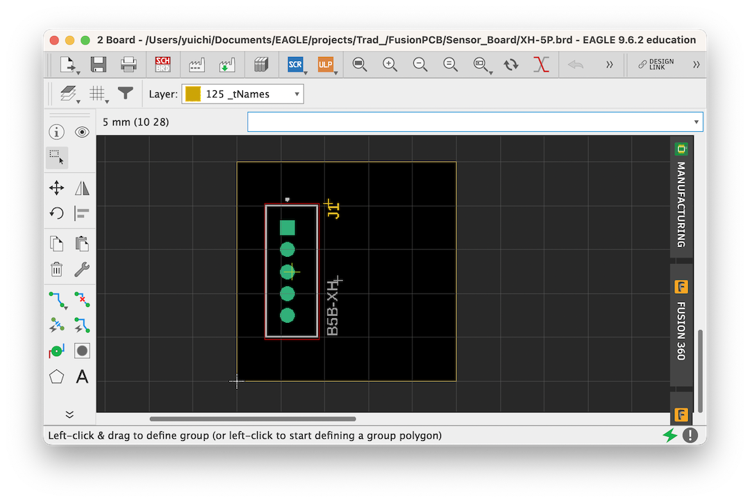
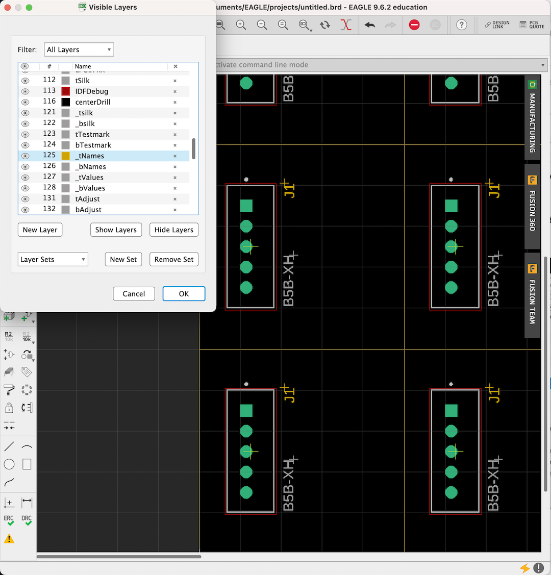
To make Gerber file, select 125_tNames, instead of 25 tName
- 25 tName continuous numbers
- 125_tName un-continuous numbers
Cost
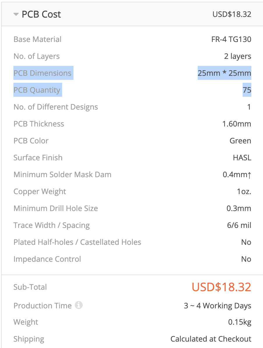
- 25 x25mm x75P: 18.32USD -> 18.32/75= 0.24USD/board
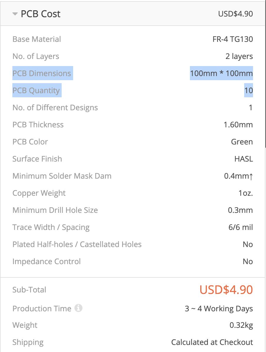
- 100x100mm x10P: 4.9USD -> 4.9/(4x4 x10)= 0.003USD/board
Round board shape
Attention
V-CUT is only accepted when the board shape is made by straight lines. But in case to make round corner shape, this is how to do it.
Ref. Round board shape_JP
It is OK if you select a line with rounded corners in 20_Dimension and draw the outline of the board. Width is 0.

20_DimensionにLineで角丸のラインを選択して基板外形を描けばOKです。Widthは0です。