6.0 Electronics Design
I have not had much experience with electronics, and this assignment hashad me very concerned. As it turns out, it was for a good reason.
This week, the group assignment was to use the test equipment in the Charlotte Latin School Fab Lab to observe the operation of a microcontroller circuit board. To see the work our group did in making these observations, please visit our page.
The individual assignment was to redraw an echo hello-world board, and add (at least) a button and an LED (along with a current-limiting resistor). To conclude this week’s assignment, we were asked to check the design rules, make the PCB, stuff it, and test that it can communicate. I was both excited and nervous about starting this week’s assignment. I like to be creative, but the electronics worry me quite a bit.
TinkerCAD– Building Backgroud Knowledge & Thinking Ahead for My Project
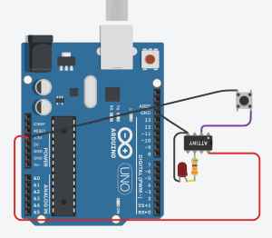
The first thing I did was go to TinkerCAD and start testing with an ATTiny and through-hole components. I assumed that I could simply replace the through-hole components with surface-mount components. One thing I have begun to think about recently was the use of a PIR Sensor, and how that could be incorporated into my final project. I would like to use an RGB LED to constantly be blinking through different colors (I haven’t planned out how many yet), but I will just stick with plain red, green and blue for now. I would like the PIR sensor to detect when either one of my grandsons enters their bedroom and to change the RGB LED to blue. I thought that this week would be a good time to start looking at RGB LED information and any codes I could find on them. I found this site, Tutorial 8: RGB LED interfacing with ATtiny85, which I plan to revisit when I work on my project later. I will use an ATTiny 412 chip instead of an ATTiny85 chip.
For a brief moment, I thought about including an RGB LED on my assignment for this week, but Tom Dubick warned me not to do this yet. Dr. David Taylor also advised me not to do it and explained that we will be coding these circuits from this week later on in multiple languages. I know that codes with RGB LED’s are at least three times as long and complicated (depending on the number of colors utilized). One other concern I had was the fact that the surface-mount RGB LED’ in our Fab Lab at Charlotte Latin School have six legs/pins on them. I was worried about not having enough pins on the ATTiny to accommodate what I needed to do for this week’s assignment. So I abandoned the idea of incorporating the RGB LED for now. The following table shows my “playing around” with TinkerCAD and what was gained by it.
| Image | Explantation |
|---|---|
 |
To just understand the wiring, I used a basic LED with a 330-Ohm resistor. (I had a breadboard in there too, but I wound up abandoning its used). I then applied a basic blink code. |
 |
I went to this project site, called Simple RGB LED Light with Fade. I assumed I could replace the Arduino with my SAMD11 and modify the components and code to my needs with the pins of the SAMDD11. |
 |
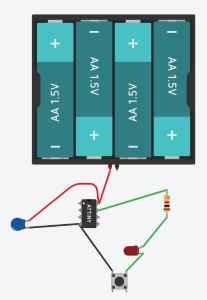
In this scenario, I started to use components that are included on the ATTiny Blinky boards that we made. I was going to start adding the switch and LED/resistor combination here and change to surface-mount components later. I thought this would give me good insight as to adding the required components for this week’s assignment |
 |
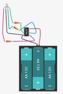
Tom Dubick assigned us this Digital Input Pull-Up Resistor tutorial as a “homework” assignment to do this week. When I completed it, I really grasped the concept of using a tactile switch as a pull-up/pull down resistor. (I actually added an LED and resistor to start simulating the parameters for this week’s assignment. |
 |
This shows how pinMode(INPUT_PULLUP) can be/was used to make a “pull-up” resistor. It reads a digital input on pin 2 and prints the results to the serial monitor as either a 0 or a 1. (A vallue of 0 in the serioal monitor means no current running through the button in the circuit; a value of 1 means current IS running through the button in the circuit.) |
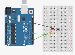
In all of the work I did this week with the ATTiny in TinkerCAD (and later with my actual circuit/PCB design), I heavily relied on Spence Konde’s pinout of an ATTiny– especially when trying to connect the pins with an Arduino.] Additionally, I used a screenshot of this pin table.
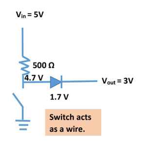
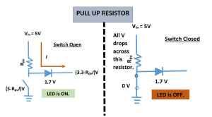
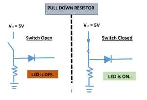
In learning how a pull-up and pull-down resistor works (electronically), I sought the help of colleague, Adam Durrett (electrical and computer engineer and AP Science instructor at Charlotte Latin School). He sat with me and talked me through it all for about forty-five minutes, and this proved to be incredibly helpful in my understanding. The following images show my (typed up/neat version) of the notes I made when working with Adam Durrett.
| |
| |
| |
|
From Adam Durrett, I learned that open and closed situations (above) have opposite outcomes (in creating “pull up” and “pull down” resistors). Electricity will always “flow” in the path of least resistance. In the “pull down” situation, the resistor has more resistance.
Designing An Echo Hello-World Board–Schematic
As mentioned above, I took a short detour this week when starting the assignment by looking into some of the potential electronics of my final project. While others thought this was negatively affecting my work, I actually gained a lot of insight for future work. Now, I began the actual task of redrawing an echo hello-world board, and adding (at least) a button and an LED (along with a current-limiting resistor).
One thing that I did do was erroneously try to make my own design from scratch. Dr. David Taylor wound up pointing out the fact that I was merely supposed to “REDRAW an echo hellow-world board that had already been created. He and I looked at the options in the Emebedded Programming Link, and I wound up choosing Dr. Gershenfeld’s Echo Hello-World Board as the board I would redraw; then I moved on to KiCAD.
This site also had this Tutorial 7: DC motor speed control using ATtiny85. I feel this site will be helpful when I program the servos in my final project.
I was thankful that I had completed Tech Explorations’ courses 4 & 5, but it had been a few weeks ago, and I wound up having to review many of the course videos when designing the schematic. I decided to call my board, a “Copycat” board. (This is how I will refer to my board from here on out). Before designing, colleague/classmate, Nidhie Dhiman helped me to install the fab academy library in KiCAD.
The first thing I did in KiCAD was bring all of the components onto the workplane. The following describes my sequence of events. Picture first, then description.
| |
| |
|
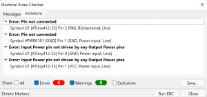
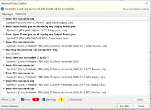
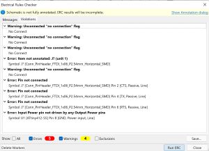
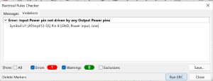
I utilized the Electrical Rules Checker (ERC) in KiCAD, but it said it was incomplete, and there were four warnings. This was actually better than an ERC check that I had done earlier that yielded 13 warnings. (There were four pins not given an “X” because they were not utilized; I was missing power and ground flags, and all of the components were missing footprints).
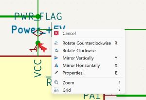
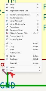
I decided to do Internet search of the error message to see how to fix the pin 1 & 8 errors. I wasn’t able to copy and paste this, so I tried to right click on it. When I did this, I got the following options:
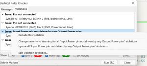
Thinking it might be best to try and fix it first, if I couldn’t find out how to delete it, I decided to have it “Ignore all ‘Input Power pin not driven by any Output Power’ pin’s violations”.
I continued to search the Internet and found this site. It stated this error could have resulted because “there is a missing connection or because KiCad has not been told where the circuit is supplied.” In further reading, it said that “it should have it’s pins Electrical Type assigned”. So I looked to find out how to do this in KiCAD.
I clicked on the “footprints”, searched, and found this:
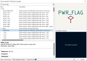
Then I tried to remove the first power flag I had after inserting the new one, and KiCAD wouldn’t let me. I conducted another Internet search “how to remove a power flag in KiCAD”, and I found this site. I really liked this site because all I had used up to this point was videos, and they are difficult when you want to refer back to something– you have to search through multiple videos to remember which video contained it. On this site, I found that I could highlight it and try to use the “Edit” button at top left of the page.
| |
| |
|
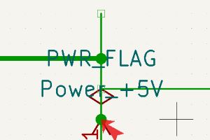
Right-clicking on this did not work.I realized the power flags were the last things I added, so I just did “Edit” –> “Undo” until they were all gone. I was then able to add a power flag at top as I wanted. I was making progress!
I learned by accident that if I highlighted the symbol and went to “Edit” at the top and selected “Cut” from dropdown, that I could remove symbols that way.
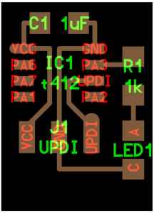
In searching through symbols, I saw that there were header pins. On Friday (March 4), colleague/classmate, Nidhie Dhiman, showed me her milled board, and she had a 6-pin header on hers. I asked her why she had a 6-pin vs. a 3-pin header, and she said she thought it might be good to have it just in case she needed more pins. I decided to add a 6-pin header as well. Now my schematic looked like this:
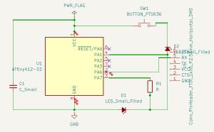
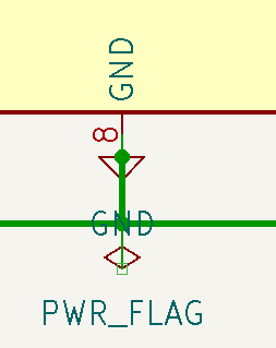
In the above picture, I realized my GND was not connected; I connected it, and ran the ERC again. This time, I got MORE errors—9 of them!
In examining all of these errors, I realized that the majority of them were because I didn’t address all of the pins on the new 6-pin header. So I added a “no connection flag” to all of them and power flags to the VCC and GND pins.
The right side of my schematic still looked terrible where the 6-header pin had been added.
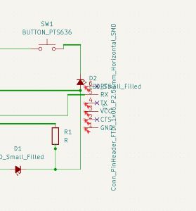
I moved the 6-pin header out more, and I moved the “no connection flags” with it since they remained where they were after moving the 6-pin header. I also deleted the VCC power flag and moved it lower down so that it (hopefully) knew it applied before the junction.
I ran the ERC again. I got rid of 4 of the errors and now only had 5:
I realized that I put the “no connection flags in wrong spot”. Since moving the power flag to the new position seemed to work, I also moved the GND flag closer in, and my schematic now looked like this:
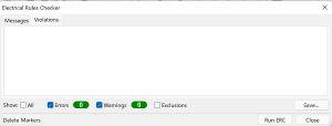
I ran the ERC again, and now only got 2 errors!
I fixed the yellow warning by deleting the “no connection flag” I had added before inserting the 6-pin header, and I tried adding another GND (below).
| |
|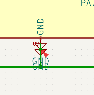
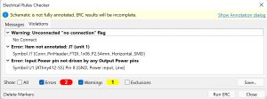
I ran the ERC again, and I only had one error left.
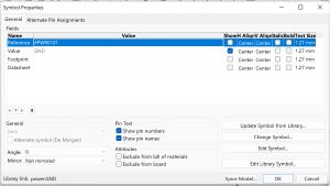
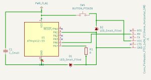
I now went to solve the final error with the GND line. Searched “Error: Input Power pin not driven by any Output Power pins” error message. Was first led back to the same site as before with the power flag issue. I read that I needed to address the pin properties. So I did a search “how to change pin properties in kicad” and got this site. I learned that I had to click on the symbol, then right click on it, and select “Properties”.
| |
| |
|
I selected “Update Symbol from Library” and saw the following image. (I had not noticed what this was doing—which is why there are two “Update symbol # PWR0101/02 FROM ‘power:GND’ to ‘power:GND’: OK”. I didn’t think this fix would be as simple, but after the previous “easy fix”, I ran another ERC. I indeed did not fix the error.
I started to think about what the error actually meant, and I remembered that all of the boards that we have milled and stuffed have had traces coming from the 6-pin header for GND and VCC. I wondered if this was the issue, so I added a wire for both going to the 6-pin header.
| |
|
From this, I knew that adding the traces to the GND and VCC pins on the 6-pin header did not do any damage electrically.
|| |
|
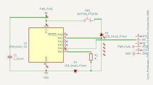
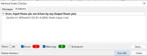
I found this site which stated: “You need to add a PWR_FLAG to the VCC and GND pins to tell KiCad that these nets are driven by an external power supply“. I wondered if the power flag I needed to add is the same one that I added on the VCC at the top of the ATTiny. So I tried it.
THIS FIXED THE ERROR, but now I had the “Schematic is not fully annotated. ERC results will be incomplete.” message again.
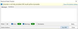
I went to add annotations again—thinking this was the issue. That was not the issue. Unrelated to this issue, in looking at the diagram, I wondered if deleting this GND would harm anything.
When I deleted it, there was an open space, so I added a wire. I then ran the ERC again.
WOO HOO!!
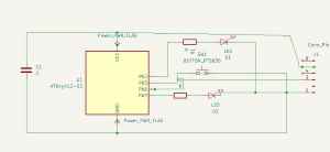
I changed all of the wire widths to 0.4 mm, as Tom Dubick had instructed us. This makes an optimal trace thickness when milling the PCB. I decided not to add capacitor (1 Uf) and resistor (1 k-Ohm) values to the schematic because they were already in the circuit, and it had to have been checked prior. In the end, the only thing I added was the push button and the additional LED.
Now I was ready to convert my schematic into a PCB. I found this site.
I went to File–> Export–> Netlist. Then I imported this netlist into the KiCAD PCB generator.
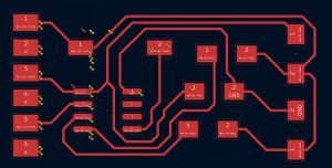
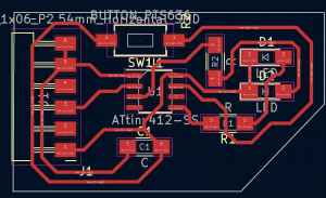
Designing An Echo Hello-World Board–PCB
When I brought the netlist into the PCB generator in KiCAD, the components all came in piled up in the upper left-hand corner. I closed the page and re-imported the netlist. This time, the PCB components were attached to my cursor, and I was able to drop them all in the middle of the PCB.
When I zoomed in, I realized that the whole thing looked terrible, and I got a sick feeling I was doing something wrong. In viewing the videos again, I began to work on placing the components on a rectangular cutout with 20.32 mm x 43.18 mm dimensions.
I tried to expand things out first to “untangle” them (the white lines are called a “rats’ nest”). This helped me to see all of the components much better. I ran the Design Rules Checker, or DRC (just to see what I will have to do). There were 16 errors and 13 warnings.
I started to run copper traces to each pad using the line tool. Midway through doing this, I ran the DRC and now I had 23 errors and 16 warnings. I was confused as to why adding the traces made it worse. I am hoping it will change as I delete the white contact “trace” lines and all of the labels. I wound up hiding all of the words and extraneous “noise” when trying to make my traces.
Then I started to change the line thickness to 0.4 mm as instructed by Tom Dubick. It also dawned on me that I could utilize the area between pins “under” the area where the chip would be positioned. As I was changing line thicknesses, I also began “rounding off” the corners.
This (above) is what the PCB looked like when I finished widening the tracks from 0.2 mm to 0.4 mm and also removing all 90-degree angles. I ran the DRC again and this time, there were 39 errors and 16 warnings! I was very concerned because I thought that as I connected the components, that the white connection lines would disappear.
Yikes! When I read the errors, I realized that the majority of them was because I have the default track width set at 0.2 mm. So I began looking around at where I could change the track width default to 0.4 mm. I went to Edit–>Track and Via Properties, and I changed the track width to 0.4 mm and ran another DRC, but there was no change. I went to File–> Board Setup and changed the “Tracks” Width value to 0.4 mm and ran the DRC again. Again, no change.
Then I saw “Net Classes” underneath “Pre-defined Size”, and I was able to see that there was a “Clearance” value that I could change to 0.4 mm. I ran the DRC, and it was now worse than before (42 errors and 16 warnings– my all-time highest!).
I started to wonder if the issue had something to do with the layers. I remembered the guy in the TechExplorations videos talking about layers. I didn’t want to go back and re-watch or fish through the videos, so I decided to copy and paste the error message and do an Internet search. I typed in “Error: Clearance violation (netclass ‘Default’ clearance 0.4500 mm; actual 0.000 mm) and kicad”. I searched the Internet and found this page; this led me to look for “Clearance” in the tools at the top. When I toggled my cursor over the tools, I saw this:
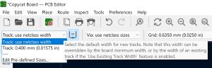
I selected “Track: 0.400 mm (0.01575 in), and I ran the DRC again. Nothing changed. At least the design rules were not violated worse!
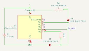
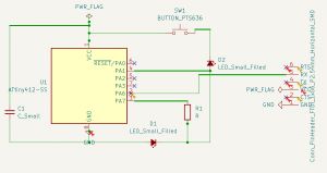
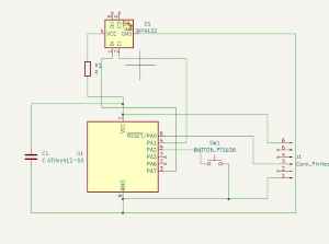
I went in on Monday morning (March 7) to get help from Tom Dubick. He examined my circuit and told me that I basically made a kill switch and that I was missing a resistor. I pulled out the switch and added a resistor for the LED I had added. However, I was still a little confused as to where I could put the switch in order to make it NOT a kill switch. My instinct is to add it to PA6 in the schematic, but I will need to ask Tom Dubick again.
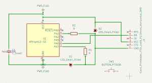
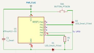
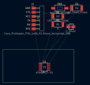
Before asking Tom Dubick for help again, I wanted to examine the two schematics side by side. The only way I could add it to the schematic at PA2. At first, I was thinking I could add it to PA0, but that is the reset pin, so I chose the next available pin. After adding the button to PA2, and connecting it to the GND pin on the 6-pin header, it made more sense to me—combining what I had learned from the TinkerCAD “digital-input-pullup-resistor” activity I did.
I ran the ERC on this schematic, and it came out with 0 issues. I was thrilled. However, I was not thrilled that I had to now completely redo the PCB design. I went back in to re-design the PCB in KiCAD. I then hid the pins that were not being used by right-clicking and selecting its “Properties”.
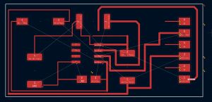
When I re-designed it, I was able to get rid of the rats’ nests. (Classmate, Charlie Horvath, showed me how to use the track lines instead of just regular lines). This was incredibly helpful. When I ran the DRC, there were numerous errors (as shown by the arrows below). I spoke to another classmate, and was told that the errors could be ignored.
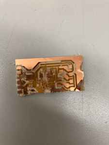
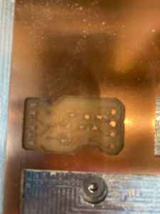
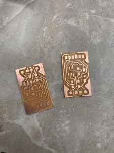
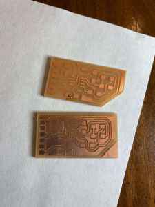
It was now time to mill my Copycat PCBs.
Milling the Echo Hello-World Board– Desktop Milling Machine
I really struggled with milling my Copycat PCB this week. The following table shows images of four failed attempts at milling my PCB.
| Image | Explanation |
|---|---|
 |
For this board, I misheard/misunderstood the pervious person who used the milling machine. What I thought was a 1/64 bit was actually a 1/32 bit. I should have used a 1/64 bit for the whole board. I pulled the PCB off of the stage, and it literally fell apart. |
 |
The depth was likely incorrect for this board. When I did deployed the bit breaking tool, it gave me a 2.1 mm depth. |
 |
The depth was likely incorrect for this board again. Also, the PCB broke when I started to scrape it off of the stage. |
 |
When I deployed the bit breaking tool, the depth was 0.02 mm. Since it was drastically different from the previous depth, I accepted the depth and tried to mill it. The bit didn’t even touch the PCB in some areas, and it scratched the other areas. |
| NO PICTURE OF THIS ONE | After speaking to colleague, Zack Buzichowski by phone about my errors, I thought I was on a good path. However, when deploying the bit breaking tool, the bit got caught on the conducting pin, and broke. I decided it was time to go home– dejected and pathetic- and try it again the next day. |
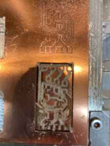
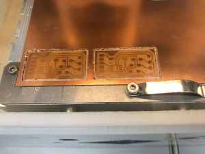
After failing five times at milling my boards, colleague– Zack Budzichowski– helped me mill two Copycat PCB’s the next day. As I explained all that had happened with my PCB’s the previous day, he stated that I likely changed the height of the material on the board each time I tried to pry a board out of the entire piece. The new boards were beautifully milled.
Stuffing the Echo Hello-World Board
As I soldered the components onto my Copycat PCB’s (I stuffed both of the PCB’s I had), I realized that on Dr. Gershenfeld’s Board, I had placed a 499-Ohm resistor where there should have been a 1-kOhm resistor. I had soldered them onto both boards, and I needed to switch them out. I got my husband– Matt Morrow– to pull the resistor up as I used two soldering irons to heat both sides. This technique worked well, and I was able to add the 1-kOhm resistor in the proper place.
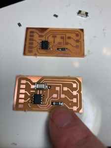
For some reason, my hands were shakier than usual, and I had to rely heavily on my tweezer tool. In the end, I was actually very pleased with how quickly (and cleanly) I was able to solder my Copycat PCB’s (in spite of having to change out a resistor).
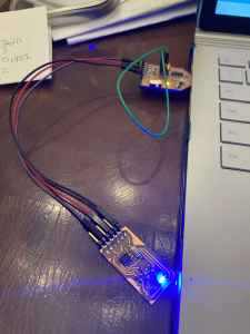
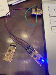
This image shows my Copycat PCB’s just after they were stuffed.
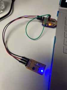
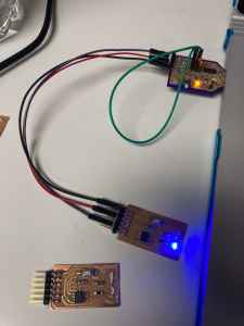
Testing the Echo Hello-World Board
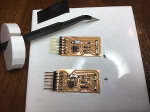
When I wired my stuffed Copycat PCB’s to my SAMD11 I noted that both of them had the blue LED light exactly the same. I was encouraged by this, and I began to test them both with a basic Arduino blink code. In the Arduino IDE, I selected the ATTiny412 as my board and my chip. (I did need to ask my classmates about this as I was still insure if I was programming my Copycat Boards correctly). I was worried that I would accidentally change my SAMD11 and have to re-program it.
| |
|
|
| |
|
When I tried to upload the Blink code to my Copycat1 Board, I got an error message.
|||
Electronics Design– The Sequel–Electronics Design That Never Dies (or Ever Really Lived?)
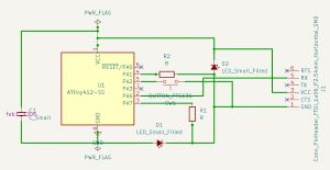
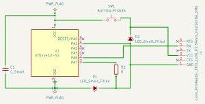
Let me emphasize again– I am not comfortable with electronics. At this point, it was Wedesday, March 9, and I sought the help of Dr. David Taylor to see why my Copycat 1 and Copycat 2 PCB’s were not working. I explained that the blue light was coming on, I thought I had made success, but I was getting a “UPDI unable to talk to the board” error. Dr. Taylor looked at the schematic, and pointed out that one mistake was that I had (once again) made a kill switch. From this statement alone, I knew I had to redesign the board once again. Before re-designing, I checked the voltages across all of the components in the boards. All voltages appeared to be appropriate.
||
That day was the day that we had the 3-hour Zoom session with Dr. Gershenfeld. I was thankful I at least had a lot on my webpage in case he called on me. That afternoon, I designed– what I now called the “CopycatWinky” PCB.
| ||
||
I milled the PCB’s after school that afternoon. At this point, milling with the desktop Other Mill machines had “clicked” with me. This was a positive outcome for all of the trouble I was having with this assignment/electronics. The image below shows the two PCB’s I milled.
We had our weekly late-night session at the Charlotte Latin School Fab Lab that night. After learning about Aspire and the CNC machine (Shopbot), I pulled the materials and stuffed the CopycatWinky PCB’s.
||
| |
| |
|
After stuffing the PCB, I quickly went into my office to test it with the Arduino Blink code.
||
Nothing worked– except for my blue LED lighting. I was so frustrated and tired. (It was about 11:00 pm at this point). I had to walk away from these PCB’s at this point.
On Thursday, March 10, I redesigned the PCB. I milled two of the boards and called it my FinalFinalBoard (even though it wouldn’t be). I was actaully confident that this design would work. I took the two milled boards (shown below) home, and went to stuff them.
| |
| |
|
||
When trying to stuff the FinalFinal PCB (in the video above), I realized that I had inadvertently cut off outside traces on them when I milled them. I thought I could try to salvage one of them by adding solder to one of its broken traces, but there was no way.
I re-examined all of the boards I had made at this point. In this examination session, I noticed that on the CopycatWinky2 PCB, I had accidentally soldered the ATTiny on the bottom upper trace (instead of on its specific copper pads).
While I am REALLY good at surface-mount soldering at this point, I felt incredibly stupid. I felt even more ridiculous in showing these two boards to Tom Dubick the next day. I had the first two lyric lines of Simon and Garfunkle’s “Sound of Silence” running through my head. “Hello darkness my old friend… I’v come to talk with you again…”. Honestly, I was numb at this point. I had the new CNC unit piling on top of all of this electronics “grime” that I couldn’t shake. Tom Dubick suggested I take a break from the electronics unit and come back to it again later.
On Friday evening, (March 11), I got a text from Tom Dubick stating that Adam Harris was going to be at the Fab Lab the next morning. He suggested that come in and meet with him; and so I did.
Returning to the RGB LED
Like the calm after the storm, I met with Adam Harris, and I swear I could hear birds singing. (Ok- it was actually his ringtone on his phone). But seriously, Adam Harris was so approachable and non-judging about all of the mistakes I had been making. I showed him all of the failed boards (stuffed and milled), and I had him look at the “FinalFinal Schematic”. He confirmed that this board should actually work.
I told him how I initially wanted to use an RGB LED, and why I had veered away from it. However, he said I actually SHOULD design the board with an RGB LED. We went into the Fab Lab and pulled the SMD RGB LED’s that I had examined ten days prior. We pulled the specs on the LED’s– which were Dotstar 5050 SMD LED’s.
Adam Harris shared links of some of the data we discussed (listed below). He had also found that two Charlotte Latin School Fab Academy students (Graham Smith Fab Academy Class of 2021 and William Zhou Fab Academy class of 2020) had included RGB LED’s in their final designs, and he suggested that I look at what they had done with them.
-
Tutorial 8: RGB LED interfacing with ATtiny85. Although this site discusses the use of an ATtiny85, I found it useful in understanding how I could implement an SMD RGB LED similarly with my ATtiny412.
-
Arduino Library Installation. I needed to install this in my Arduino libraries.
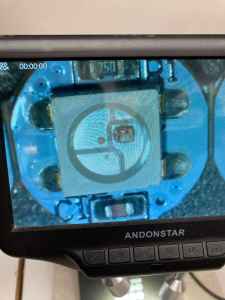
In the Charlotte Latin School Fab Lab, there were two types of SMD LED’s, one that had 6 “legs” and one that had “four legs”. Mr. Nelson (from Central Piedmont Community College) was also at the CLS Fab Lab and overheard Adam Harris and I talking about the SMD RGB LED’s. He suggested we try the 4-legged ones. However, the ones that we had in the Fab Lab were mounted onto a board. Adam Harris and I tried to remove them from the boards they were mounted on, and eventually abandoned this because we were melting the plastic. (We didn’t want to damage the LED’s).
||
We examined the back of the 6-legged LED’s with the microscope and found that they had a 750-Ohm resistor in them.
I talked through the schemtic and PCB design with Adam Harris, and we realized I had used the wrong footprint for the SMD RGB LED. I was glad that I had run it past him before milling the PCB’s. The images below show the final outcome.
| |
|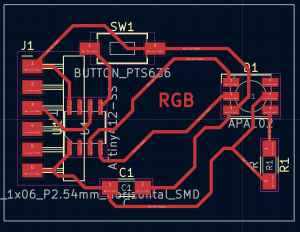 |
|
This video shows me stuffing the two RGB LED PCBs.
||
I went to test the RGB LED PCB’s, and I (naively) used the code that I had found at the start of this unit. I realized that I needed to change the pins and tried modifying the code.
||
The good news with this test of the two boards is that the code indeed uploaded to both of the boards, and I knew this because I got the “Done Uploading” message. I emailed Adam Harris, who quickly pointed me to the correct code and how to modify it with the proper pins on the ATTiny.
I went in to the Fab Lab (now Sunday, March 13), and I asked Tom Dubick to help me figure out why my LED was not lighting. He tested the voltages of the components, and they were indeed correct. We also used Adam Harris’ email to make sure we had the proper code. In this video, we were able to demonstrate a properly programmed and functioning PCB.
||
During the week of our spring break (March 11-18), I worked to get the LED’s working on my “FinalFinalBoard”. I decided to mill and stuff two more with the modifications, and I actually had success! (OK- not right away).
||
I thought I had fixed the errors I had in previous boards– not noticing the huge mistake I had made. Honestly, at this point, I have made so many boards, I am pretty sure I am not naming them correctly.
As I examined and compared the pinouts for both the ATMega328 and the ATTiny412 chips, I realized that I never connected any of the pins on the 6-pin header to the UPDI pin on my ATTiny412. I live far away from the Charlotte Latin School Fab Lab, and I decided to troubleshoot the PCB with the materials I had with me. I used a small jumper wire and soldered the second pin on the 6-pin header to the UPDI pin (PA0, and Arduino pin 5). It wasn’t pretty, but it worked. The “Combined (Arduino) Code” is attached below.
||
New Skill This Week
One final thing I learned in this week’s work is how to embed videos in an easier way from this link.
Again, this week, the group assignment was to use the test equipment in the Charlotte Latin School Fab Lab to observe the operation of a microcontroller circuit board. To see the work our group did in making these observations, please visit our page. To see my work on this group projectm please visit this site.