4.5 Group Project- Electronics Production
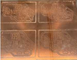
For our group project this week, we were tasked with characterizing the design rules for our in-house PCB production process at the Charlotte Latin School Fab Lab. Our group met on Tuesday evening to learn how to use the milling machines (Other Mills) and their (Bantam) operating software. Tom Dubick had used KiCAD to design a circuit for an MVP PCB using an ATTINY412 chip. On Tuesday evening, Avery, Scott, Charlie and I sat down to individually mill boards. This was the first time I would be doing it alone. I decided to use the second milling machine in the CLS Fab Lab, and I followed the steps above. I chose to start milling the ATMEGA328 PCB designed by Adam Harris. The image below shows the PCB’s that I cut.
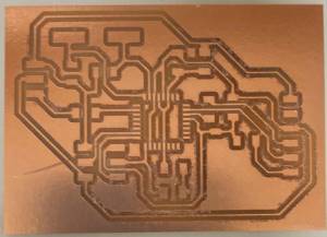
This image shows a close-up of one of the PCB’s. The chatter can be clearly seen.
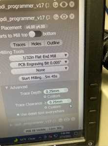
Tom Dubick showed me how to use the “Advanced” tool to modify the next cut. The image below shows how he had modified the Advanced settings to make the bit carve deeper into the prototyping board.
Using a metal scraper, I scraped the PCB’s off of the metal plate. I then cleaned the PCB’s and noticed that the only one that did not have evidence of “chatter” (eratic vibrations when cutting that cause trace lines to be “sloppy”). Three of the PCB’s had pieces of copper that actually came off when I removed them from the metal plate.
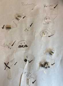
On that same evening (Wedesday, February 15), Avery, Charlie and Scott and I found and pulled all of the components needed to stuff our ATMEGA 328 PCB’s. The image below shows this.
The next day, on Wednesday afternoon (February 16), colleague/classmate, Scott Moulton and I decided to mill more of the ATTINYMEGA328 PCB’s. We had both had chatter on the PCB’s we had cut the night before, and we wanted to see if we could improve. We followed the steps above, but this time, colleague Zack Budzichowski suggested that we check the heights of the prototyping board that was affixed on the metal plate. After examining the metal bed plates on the other machines, you could see that the boards get damaged easily. For example, using the metal scraper actually causes scrapes in the metal place. Other inconsistent material height can also be attributed to errors made on the milling jobs–like using the wrong bit, or improperly measuring and entering the thickness of the material into Bantom software.
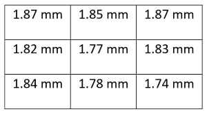
To test the metal plate bed height, we divided the prototyping board into a 9-square grid. In each grid, I deployed the Bit Breaking tool to measure the height of the material. The following table shows the values of each area in the grid. The front of the board is the bottom of the table.
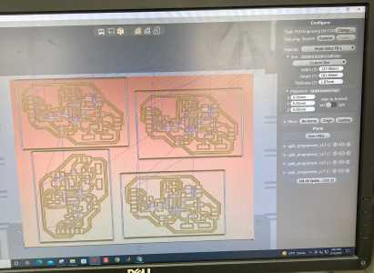
Based on this information, Scott and I decided to arrange the PCB’s into positions that had similar values. The image below shows how we arranged them.
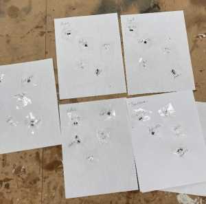
As we were leaving school for a long weekend, I assembled the components that everyone would need for the ATTINY MVP PCB designed by Tom Dubick for all of our group members. I pulled the components from the CLS Fab Lab, and I taped them onto five pieces of white computer paper (one for each member of our team) and labeled the components. The image below shows this work.
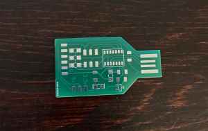
This site shows how to order production quality PCB’s. Nidhie Dhiman sent our SAMD11 PCB to be professionally manufactured. The image below shows the professionally manufactured SAMD11 PCB.
To see our group work, please visit our page, Electronics Production- In-House PCB Process.