14.0 Networking and Communications
This week, our indivisual assignment is to design, build, and connect wired or wireless node(s) with network or bus addresses.
Networking Research
Before starting any work this week, I had to do a lot of research (articles and videos). The following list shows all of the sites I visited.
Videos
What is I2C, Basics for Beginners
I2c Protocol (Animation + Programming) atmega8 amtega16 atmega32– This site had a great animation of how the bits are sent through the SDA line driven by the SCL line.
I2C Communication on the Atmel SAM D21 Xplained Pro Board using the TE TSYS01 Temperature Sensor
Lecture 3.1 Wire Library– I got this video from Aaron Logan. Although it is short, it was incredibly helpful.
Articles
I2C Bus for ATtiny and ATmega– This site includes some of the coding language at the bottom… I don’t always trust Instructables, but it seemed to match what I saw/read on other sites.
A Guide to Arduino & the I2C Protocol (Two Wire)
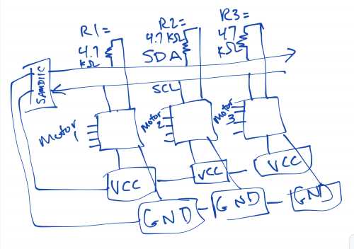
After reading the articles, viewing the videos mentioned above, and digesting the information, I needed to visually draw out what I intended for my designs to look like this week. The following image shows my initial thoughts in a quick sketch I drew in the Notability app on my iPAD. Since I intend to connect a stepper motor to each of the “nodes”, I knew that four pins would be needed for this. I also wanted to include the PIR sensor and RGB LED in my designs.
I then began to design my PCB’s. I refuse to use the terms “Master” and “Slave”. Instead, I will call my PCB’s “Parent” and “Child x” respectively.
Designing
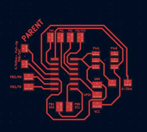
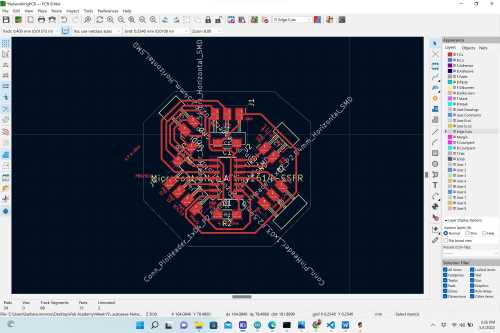
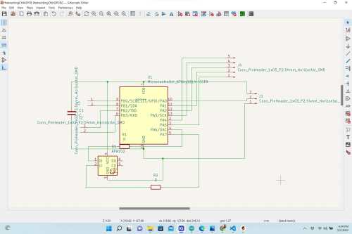
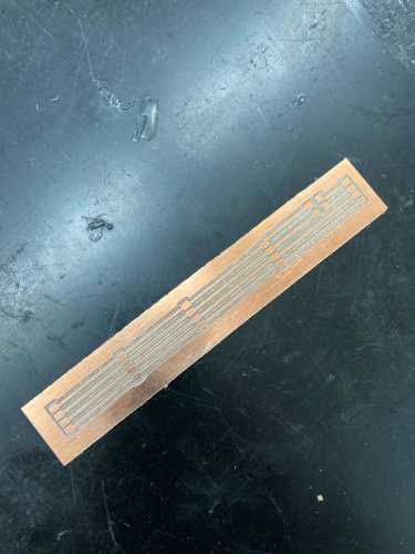
I opened KiCAD, and the first thing I started to design was the Parent PCB. Since I plan to use these boards for my final project, I wanted to make sure that the PCB’s used this week to be adaptable. Since the ATTiny1614 chip has more pins than the ATTiny412 chip, I decided to utilize it in all three of my PCB’s. The images in the following table show my progression in designing the Parent PCB.
| Image | Description |
|---|---|
 |
First, I placed an ATTiny1614 chip and connected a 2-pin header to the SCL and SDA pins. I knew there needed to be a resistor, so I added one on pin |
 |
I added a 3-pin header for the VCC, UPDI and GND. |
 |
I added another 2-pin header to isolate the RX and TX pins together. |
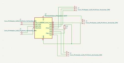 |
I then used two 3-pin headers to simply “pin out” the remaining headers to use with sensors (like the PIR sensor). |
 |
Before beginning the PCB design, I decided to look at some of the examples on the Fab Academy website to see if I was on the right track. I viewed this diagram, and realized that needed the capacitor. |
 |
I realized (when designing the PCB for the parent board) that I did not add two, 4.7 k-Ohm resistors as pull-up resistors along the SDA and SCL lines in the bus. I was very excited about the deigned parent board schematic because it really did not take long to design. I assumed the PCB would be equally “easy”; that was a poor assumption. |
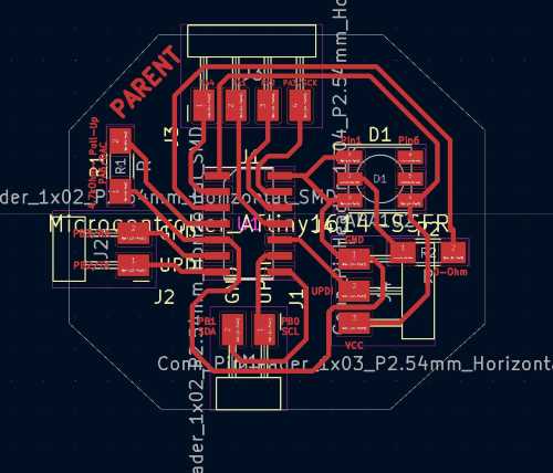
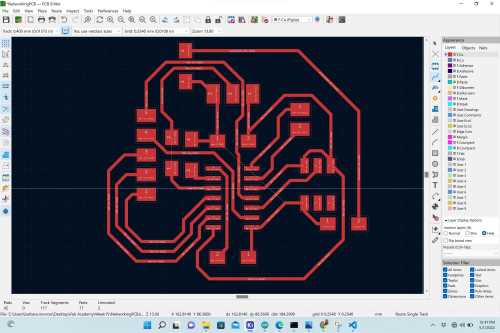
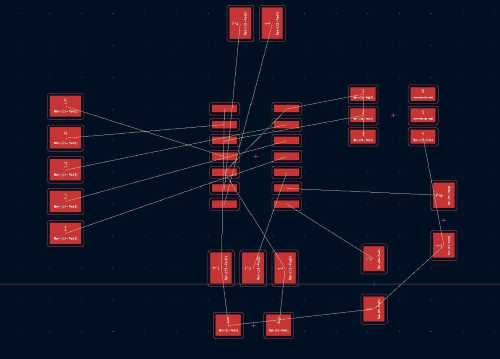
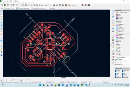
When I loaded the Parent Schematic into the KiCAD PCB designing interface, I had to keep going back to the schematic, and I greatly struggled with with clearing the rat’s nests each time. The following images show the progression in designing the Parent PCB.
| Image | Description |
|---|---|
 |
Before heading to the PCB interface, I tried to add an APA102 (50/50) RGB LED to this board (with the hope of using this board in my final project). It was fairly easy to add it, but this addition wound up being problematic in the end. I struggled for about two hours in trying to make the PCB work, and I eventually wound up adding a 0-Ohm resistor that allowed me to “jump” the VCC line. |
 |
I thought I was all set with this design, and I labeled it (to try to prevent having to look up which pins were connected under the ATTiny1614 cip). As I looked at this design, I remembered that with the RGB LED PCB a few weeks ago, I had left off the reisitors. So I went back and added them in the schematic. |
 |
In this PCB design, I added the two needed resistors for the RGB LED. |
 |
After adding the two resistors for the RGB LED, this is what the rats’ nest looked like, and I began to clear it. Sadly, as I worked through this process, I also noticed that the SDA and SCL pins both needed the pull-up resistors added. |
 |
This is what (I thought) the final parent PCB would look like. I worked on this design for over six hours, and I started over at least seven times. Very frustrated, I wound up removing the RGB LED and decided to try to add it to one of the Child boards. Once the RGB LED was gone, it was easy to just add the footprint for male headers on most of the pins. |
 |
This shows how much easier the new PCB was without the RGB LED in the design. |
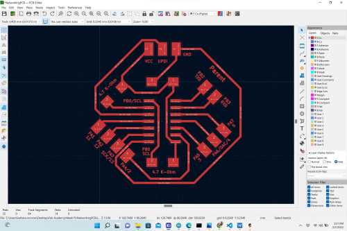 |
As I was wrapping up the parent board, I discovered that I had left off male header pins for the SDA and SCL lines. I felt really absent-minded as these were the two most important parts of the whole I2C design. |
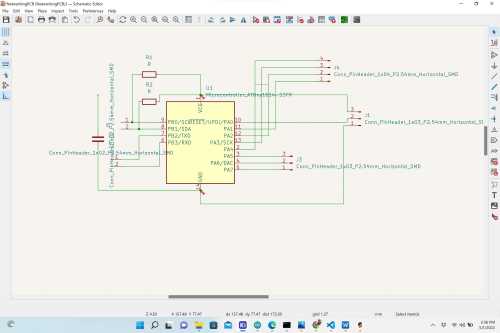
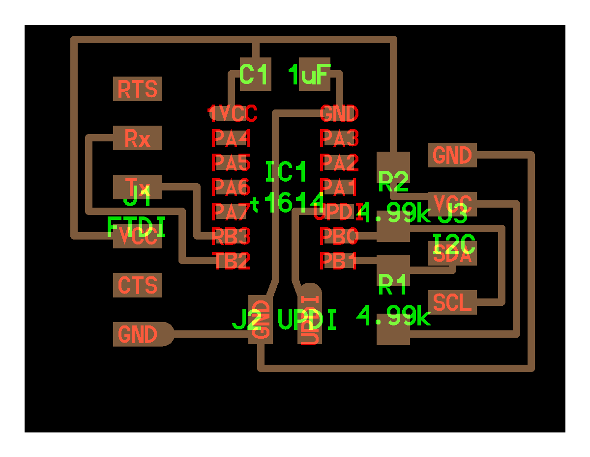
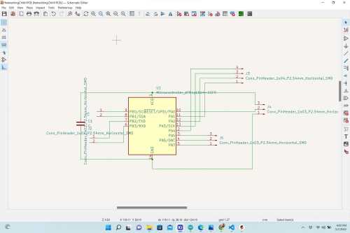
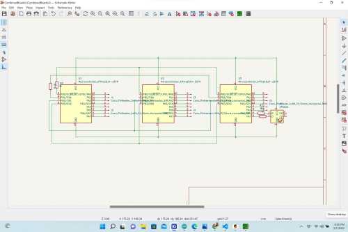
Now it was time to begin designing the two child boards. I was so weary of the designs at this point (from all of the problems I had with the parent board), I wanted to make this PCB a little simpler. It is mainly just all fourteen of the pins connected to male headers. The following diagram shows my schematic for Child 1.
As previously mentioned, I wanted all three of the boards to be versatile in the end so that I could utilize them in my final project. I again chose to use ATTiny1614 chips (for both) since they can handle more code (have more memory) than the ATTiny412. In the end, I would like to possibly add one stepper motor to each PCBand use networking with the three of them. I really wanted to add the RGB LED back into the design of one of the boards, so I added it back in to Child 2.
 |
 |
|---|---|
| Child 2 Schematic– embarassingly, I forgot the resistors again on the RGB LED. This shows them added properly. | Child 2 PCB– this was easier to create. I think it was easier because the external pull-up resistors were not on this board (since they only have to be utilized with the parent). I also decided to use four 0-Ohm resistors ro help. |
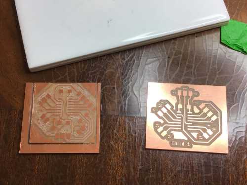
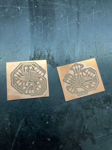
On Sunday, May 1, I finished the schematics and PCB designs on the way home from the beach. It was time to mill the PCB’s, and after the long drive home, I went into the Charlotte Latin School Fab Lab to use the desktop Othermill machines for milling them.
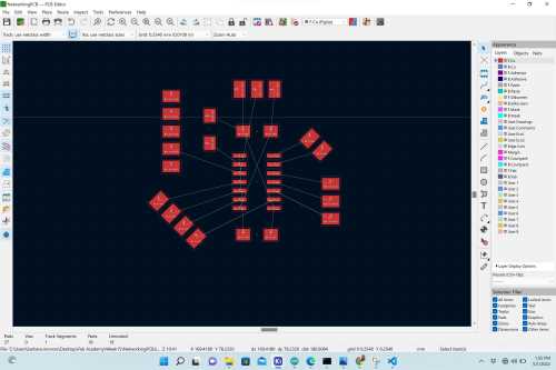
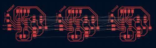
Colleague and classmate– Nidhie Dhiman– was also there milling her PCB’s. As Nidhie and I discussed networking, I mentioned to her that I wanted to make a PCB with all three of the chips on one board and eliminate a lot of the wires. As the boards were milling in the desktop Othermill milling machine (and I watched them), I started to play around with a combination design in KiCAD.
 |
 |
|---|---|
| Since the boards had already been designed, I was quickly able to copy and paste the three PCB’s into one combined board. (Although I wasn’t sure if it was correct). | Once I saw the rats’ nests in this board, I was pretty depressed. I abandoned this idea at that time. |
Testing
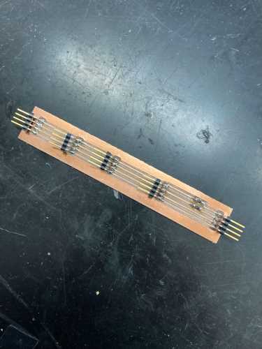
Nidhie and I had spent nearly seven hours at the lab discussing the work we were doing and milling the PCB’s. After a long day, I gathered the components for stuffing the three PCB boards (the “Family”) and headed home. The following video shows me stuffing the three PCB’s that night. I knew that Dr. Adam Harris was coming in to meet with us on Monday after school, and I wanted to have all three of the PCB’s ready in case I encountered any problems with them.
This is what the three PCB’s looked like when I had finished stuffing them all.
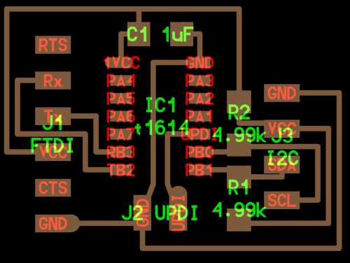
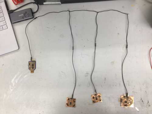
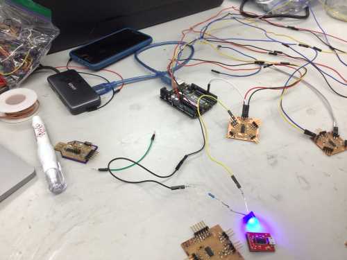
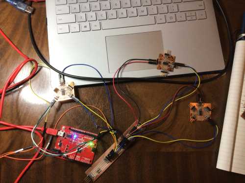
On Monday, May 2, Just to see what it all would look like, I quickly wired them up together to see what I was going to be dealing with. I knew that I needed to connect the nodes in parallel with the parent board and I that I would need four “line” wires. The following image shows how I quickly wired the PCB “family” together.
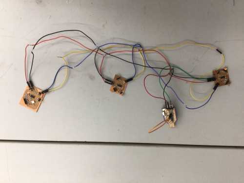
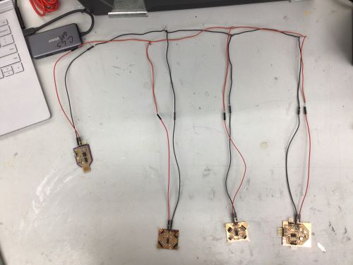
I felt like this wiring was going to be difficult to manage, I decided to make– what I would eventually call– a “harness” for the three PCB’s. I designated specific colors to code the wires (Red = VCC; Black= GND; SCL= Yellow; and Blue= SDA).
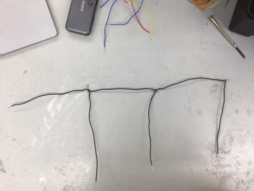
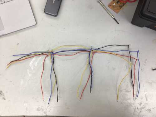
The following images show the progression in making the wire harness.
 |
 |
|---|---|
| I started with cutting and soldering black solid core wires to form the GND line. I eventually wanted the option to add a third node (for the group project), so there are lines for my two nodes/”children” and a third node. | I repeated this process (of cutting and soldering wires) with red, yellow and blue solid core wire. |
 |
 |
|---|---|
| I connected the parent and child 1 and child 2 to the GND wires. | I also connected the parent and child 1 and child 2 to the GND wires. |
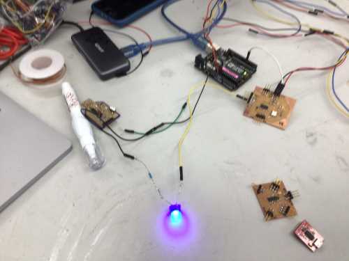
This image shows the fully wired parent with child 1 and child 2 PCB.
Before Dr. Harris arrived, Nidhie Dhiman and I were having discussions with classmate–Aaron Logan. The three of us debated about all of the things we needed in our networking designs. Aaron was using an ATTiny1614 chip, and Nidhie was using an ATTiny412 chip. Aaron mentioned that he was not using external pull-up resistors on his SDA and SCL lines since the ATTiny1614 had built-in internal pull-up resistors. I was now second-guessing my PCB design.
That evening, Dr. Adam Harris arrived for a help session. Prior to his arrival, Aaron Logan and Nidhie Dhiman had been discussing how we could find out the ID# on the ATTiny1614 chips. After an Internet search, I found
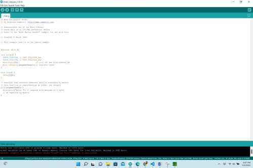
I used the arduino code to make my SAMD11 a “non-programmer” (code is shown below in another section), and then I uploaded the “I2C_Address_Finder”.
// i2c_scanner
 //
 // This program (or code that looks like it)
 // can be found in many places.
 // For example on the Arduino.cc forum.
 // The original author is not know.
 //
 // This sketch tests the standard 7-bit addresses
 // from 0 to 127. Devices with higher bit address
 // might not be seen properly.
 //
 // Adapted to be as simple as possible by Arduino.cc user Krodal

#include <Wire.h>

void setup()
{
    Wire.begin();
    Serial.begin(115200);
    Serial.println("\nI2C Scanner");
}

void loop()
{
    byte error, address;
    int nDevices;

    Serial.println("Scanning...");

    nDevices = 0;
    for(address = 0; address <= 127; address++ )
    {
        Wire.beginTransmission(address);
        error = Wire.endTransmission();
        if (error == 0)
        {
            Serial.print("I2C device found at address 0x");
            if (address<16)
                Serial.print("0");
            Serial.print(address, HEX);
            Serial.println(" !");
            nDevices++;
        }
        else if (error==4)
        {
            Serial.print("Unknow error at address 0x");
            if (address<16)
                Serial.print("0");
            Serial.println(address,HEX);
        }
    }
    if (nDevices == 0)
        Serial.println("No I2C devices found\n");
    else
        Serial.println("done\n");
    delay(30000);
 }
When I ran this code with my ATTiny1614 boards, all addresses (up to 127 of them) appeared.
In talking to Adam Harris, we looked at the data sheet– page 365 (of 598!)– and learned that we have to physically assign the ID address for the ATTiny1614 chip. We found this information on page 365 of the 1614 Datasheet.
Then, Dr. Harris explained I2C networking to the whole group, and I recorded this “lecture” so that I could go back and review his notes if needed. I also shared the video with the others in the Charlotte Latin School Fab Lab.
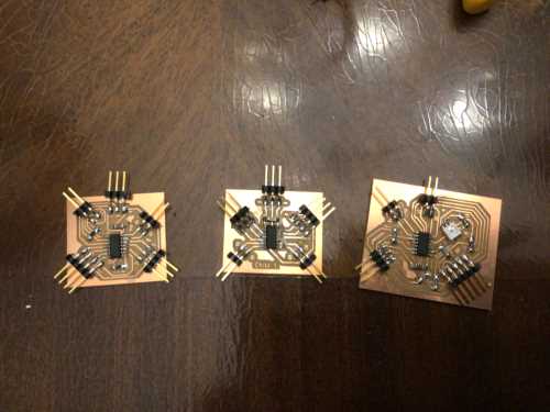
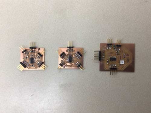
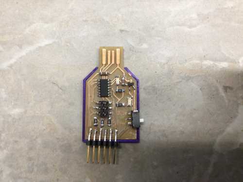
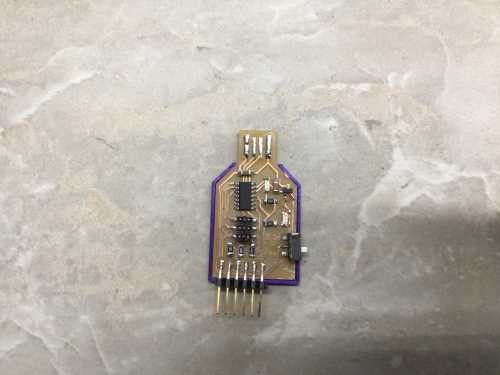
After this meeting with Dr. Harris, I was feeling much better with the content of networking. As we all started testing our designs, Dr. Harris asked for a PCB that he could try to program using I2C. I gave him my Child 2. After he examined Child 2, he realized that the GND pin was not connected to anything. I had to either re-design Child 2 again, mill more of the parent or Child 1 to replace it, or I could use a previously designed board to replace it. I decided to re-mill the parent board and the Child 1 board again. Child 2 was so similar to the PCB that I had made in the previous week (for Inputs with the PIR sensor), I decided to make that board “one of the family” and re-mill Child 2. I quickly stuffed the newly cut PCB and went to test them. The following image shows the PCB’s (parent on the left, child 1 in the middle, and child 2 on the right).
The entire group of Charlotte Latin School students were asked to wire three Arduino’s together and get them to “talk”. Using A Guide to Arduino and the I2C Protocol, classmates Aaron Logan and Nidhie Dhiman and I were able to complete the task. I decided to try the same three codes with my boards (shown below).
Parent Code
// Wire Controller Reader
// by Nicholas Zambetti <http://www.zambetti.com>

// Demonstrates use of the Wire library
// Reads data from an I2C/TWI peripheral device
// Refer to the "Wire Peripheral Sender" example for use with this

// Created 29 March 2006

// This example code is in the public domain.

#include <Wire.h>

void setup() {

  Wire.begin();        // join i2c bus (address optional for master)
  Serial.begin(9600);  // start serial for output
}

void loop() {
  Wire.requestFrom(4, 2);    // request 6 bytes from peripheral device #8

  while (Wire.available()) { // peripheral may send less than requested
    char c = Wire.read(); // receive a byte as character
    Serial.print(c);         // print the character
  }

  delay(500);

   Wire.requestFrom(8, 6);    // request 6 bytes from peripheral device #8

  while (Wire.available()) { // peripheral may send less than requested
    char c = Wire.read(); // receive a byte as character
    Serial.print(c);         // print the character
  }

  delay(500);
}
The codes used for each of the child boards were identical except for two lines.
Code for Child 1
// Wire Peripheral Sender
// by Nicholas Zambetti <http://www.zambetti.com>

// Demonstrates use of the Wire library
// Sends data as an I2C/TWI peripheral device
// Refer to the "Wire Master Reader" example for use with this

// Created 29 March 2006

// This example code is in the public domain.

#include <Wire.h>

void setup() {
  PORTB_PIN0CTRL |= PORT_PULLUPEN_bm;
  PORTB_PIN1CTRL |= PORT_PULLUPEN_bm;
  Wire.begin(8);                // join i2c bus with address #8
  Wire.onRequest(requestEvent); // register event
}

void loop() {
  delay(100);
}

// function that executes whenever data is requested by master
// this function is registered as an event, see setup()
void requestEvent() {
  Wire.write("hello "); // respond with message of 6 bytes
  // as expected by master
}
Code for Child 2
// Wire Peripheral Sender
// by Nicholas Zambetti <http://www.zambetti.com>

// Demonstrates use of the Wire library
// Sends data as an I2C/TWI peripheral device
// Refer to the "Wire Master Reader" example for use with this

// Created 29 March 2006

// This example code is in the public domain.

#include <Wire.h>

void setup() {
  PORTB_PIN0CTRL |= PORT_PULLUPEN_bm;
  PORTB_PIN1CTRL |= PORT_PULLUPEN_bm;
  Wire.begin(4);                // join i2c bus with address #4
  Wire.onRequest(requestEvent); // register event
}

void loop() {
  delay(100);
}

// function that executes whenever data is requested by master
// this function is registered as an event, see setup()
void requestEvent() {
  Wire.write("hi "); // respond with message of 2 bytes
  // as expected by master
}
Using my SAMD11 PCB and what I remembered doing the previous week with my PIR sensor, I repeated the same procedure from that week to upload the codes from the Arduino activity onto each board. The codes seemingly loaded onto the boards, but I was unsure of how to view the words “hello” and “hi” from each board. I knew I had to make my SAMD11 a “non-prorgammer”, and I went to Dr. Harris’s page– SAMD11C Multi-use Board to retrieve the code (shown again below).
Code for making my SAMD11 a Non-Programmer:
void setup() {

   SerialUSB.begin(0);
   Serial1.begin(57600, SERIAL_8N1); //Adjust baud rate and use SERIAL_8N1 for regular serial port usage
}

void loop() {
   if (SerialUSB.available()) {
      Serial1.write((char) SerialUSB.read()); //Send stuff from Serial port to USB
   }
   if (Serial1.available()) {
      SerialUSB.write((char) Serial1.read()); //Send stuff from USB to serial port
   }
} //end loop
Nothing that I did that night seemed to work. I noticed that my computer screen was starting to flash a “gltichy” pixelated screen every time I plugged and unplugged my SAMD11 board. After examining the SAMD11 board, I realized that the copper traces were beginning to wear down. While Dr. Gershenfeld does not approve of adding solder to the USB area of the USB connectors, I was very concerned about losing this board, and I need it for my final project. (We do not have any more SMD 3.3V regulators in the Charlotte Latin School Fab Lab, and we are unable to get them ina timely fashion due to supply chain issues). So I went into the soldering room and added more solder to the worn copper lines.
 |
 |
|---|---|
| My SAMD11C board with worn-down copper USB lines | My SAMD11C board after adding solder to the USB lines |
I decided to leave the lab that night (at 11:00 pm) and try again tomorrow. In the meantime, I actually tried to combine all three of my boards into one “Mother” board.
|
|
|---|---|
| Combine Schematic– much easier to design than the PCB | PCB with rats’ nests– much harder to clear. This was never developed beacuse of the amount of time it would take to fully complete. |
On Tuesday, May 3, I was still having trouble seeing the code in the serial monitor. The following video shows what I was doing.
I had been using my SAMD11, and Tom Dubick suggested I try using my Arduino board (converted into a UPDI programmer with jtag2updi code) to use the serial monitor. I have always been confused by the jtag2updi programming, and I am very comfortable using my SAMD11– since I have been using it for so many weeks. Dr. Fagan came in to the lab for a weekly visit with us, and I was able to sit down and trouble-shoot a little with him.
After hearing the troubles I was having, Nidhie Dhiman suggested that we load and run a simple “blink” Arduino code on each PCB connected to an external LED to see if the chips were functioning properly. The following images show that all three of my boards were indeed working with properly functioning chips in them. I used the Arduino with jtag2updi programmer to upload codes onto each chip.
I then milled two new boards, and decided to change out two of the previously milled and stuffed boards with them.
 |
|
|---|---|
| Two new, freshly milled PCB’s. | The new “family” of PCB’s I planned to test. |
While still at school on Tuesday, since I had so many wires to deal with, Dr. Fagan suggested that I combine the four wires (SDA, SCL, GND and VCC) together into one unit. I showed him how I had started designing a combination board, but he clarfied that I should just make a “bus” breakout board with only SDA, SCL, GND and VCC. I wound up leaving the Charlotte Latin School Fab Lab not feeling well, and the next morning, I stayed home from school.
While at home, I continued to work on troubleshooting and testing my PCB’s. The following video shows me stuffing the new PCB’s from Tuesday night.
This videos show the sequence of me testing the newly stuffed PCB boards, and eventually having some success.
This is the link that led me to the need for FTDI drivers, called Attiny1614 Serial. print. I also found info about needing the drivers at this site: How to Install FTDI Drivers and Drivers: Home / Drivers.
The following video shows me stuffing the third round of PCB’s I milled (on Thursday).
These are the new boards I milled:
I also designed and milled a “bus” for connecting all of the nodes– parents and children– as Dr. Fagan had suggested. With this board, I was hoping to remove some of the lengthy (and at times, confusing) wiring.
 |
 |
|---|---|
| This shows the bus just after it was milled. | This shows the bus after it was stuffed with two 4.99-Ohm resistors (on the SDA and SCL lines). The four lines on this bus are: VCC, GND, SDA and SCL. |
I used the following “snippet” of code in my arduino scripts off and on as I methodically tested my boards. This bit of code turns the internal resistors in the ATTiny1614 chip “on” and “off”.
  PORTB_PIN0CTRL |= PORT_PULLUPEN_bm;
  PORTB_PIN1CTRL |= PORT_PULLUPEN_bm;
In the middle of the night, I couldn’t sleep, so I decided to work on my assignment for next week. As I sat down at my dining room table, I had an old Arduino Uno (from Sparkfun) that I used to use when I taught Girls Who Code. I noticed that this red Sparkfun Arduino Uno was different from the black Elegoo Arduino Uno I had been using in that it had actual SCL and SDA pins labeled in the upper right corner. I wondered if I could get my parent and two children to actually work on this board. So I started to play around with it.
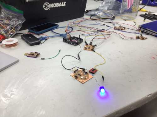
I uploaded the 2-line “snippet” of code above into the parent code, and loaded the code onto the parent board using the (Elegoo) Arduino Uno that had been converted into a jtag2updi programmer. I also used this board to make sure that code 1 was loaded onto child 1 and that code 2 was loaded onto child 2. I then used the red (Sparkfun) Arduini Uno to serve as a power source and for the serial monitor. I decided to test one child board at a time, starting with child 1, and I systematically tested the wiring. To prove that the red (Sparkfun) Arduino Uno was not serving as the parent, I uploaded a generic blink code to blink the built-in LED onto it. Nothing seemed to be working until I happened to test whether the TX on the parent board should be connected to the TX pin on the Arduino Uno, and the RX pin on the parent board should be connected to the RX pin on the Arduino Uno. IT STARTED TO WORK!!!!
The word “hi” started to appear in the serial monitor! I was so excited, but it was nearly 2 am. I quickly got video of the parent and child 1 functioning properly together. Then, my next task was to determine if child 2 could be added to the bus. Once again, using the black Arduino Uno that had been converted into a jtag2updi programmer, I uploaded the proper code for child 2. When I connected it to the bus with child 1 and the parent board, it wasn’t working at first. Then, I realized that I had the SCL and SDA wires reversed! Once I connected it properly, the words “hihello” began to flash across the serial monitor. I had both children working and communicating with the parent board. The following video shows all of this with an explanation of the wiring.
This video shows further proof that the parent and children were themselves communicating. I hit the reset button on the red (Sparkfun) Arduino Uno– which is also a clink code uring the built-in LED.
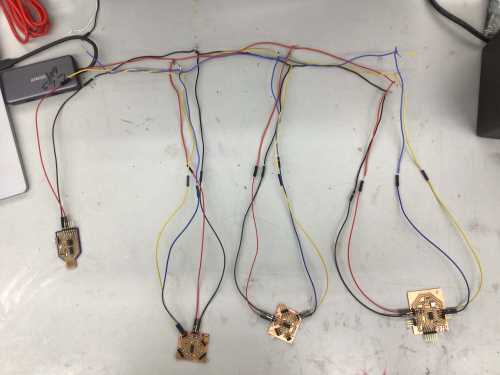
This image shows the wiring for my parent, child 1 and child 2.
This week, our group assignment was to send a message between two projects.
To see our group’s documentation, please visit this site. To see my work on this group assignment, please visit [this page](https://fabacademy.org/2022/labs/charlotte/students/barbara-morrow/assignments/week14b/].