16.0 Wildcard Week– Forming Circuits on Different Materials
I have been waiting for this week for a very long time. Way back, during the Electronics Production week (as painful as it was to me), I wanted to start designing circuits that could be cut in either acrylic or glass. As I learned how to use KiCAD, I had to then use the desktop milling machines to cut the PCB’s. Using the milling machines took me forever to understand what I was doing in the settings. I am not sure why it took me so long to fully understand Bantam software and Other Mill Milling Machines. I kept thinking to myself “it would be really cool if I could just laser cut these circuits”.
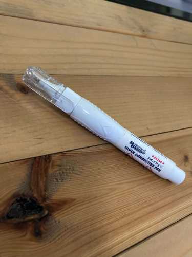
In the middle of that week, I was so inspired by the thought of this that I went online and purchased an MG Chemicals Silver Conductive Pen.
I watched the following videos as inspiration.
Clear flexible printed circuits - first success– In this video negative imprints and a lot of chemicals are used.
Creating Easy Glass Circuit Boards at Home– Although the woman in this video is speaking in French, and I only understood about three words, I still understood what she was doing. I would like to also try this method using metally/conductive adheasive copper tape.
I also found this website–PCB on Glass– This tutorial shows how to make circuit designs on bendable plastic. This idea interested me a lot, but it too required a lot of chemcials. I would like to try this method curved 3D circuits could be created using this technique.
I looked at all of my PCB’s that I have right now. I make all sets of PCB’s in pairs. I have 34 PCB’s in total. (Yes, 34). Some of them worked, many of them didn’t.
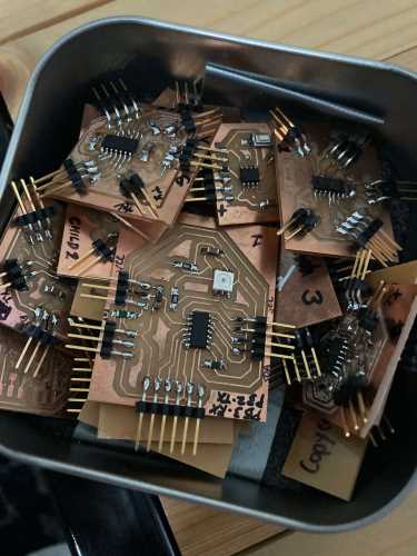
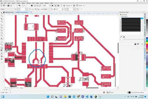
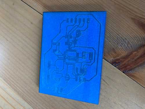
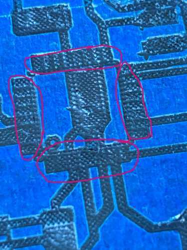
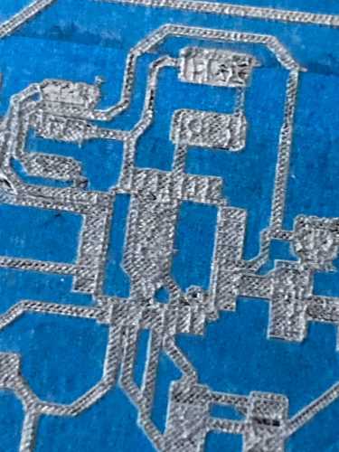
Feeling like I was rummaging through an old yearbook, I began looking at all of the PCB’s closely. I was searching for one that was (seemingly) simple and one that was more complex in design. I decided that the ATTiny 412 MVP (created by Tom Dubick) and the ATMega 328 (created by Adam Harris) PCB’s would be my polar opposites in terms of complexity. In looking at the ATMega 328 again, I really liked the way that circuit was designed– it had some very beautiful curves and diagonal lines of symmetry. (And out comes my minor in art). The ATMega 328 chip was the most difficult one for me to solder. Since it has 32 pins that are very close together, I was worried about how the laser cutter in the Charlotte Latin School Fab Lab would raster it. I also was worried that rastering the pins in the acrylic would melt them together. But I wanted to try this out and see how it would work.
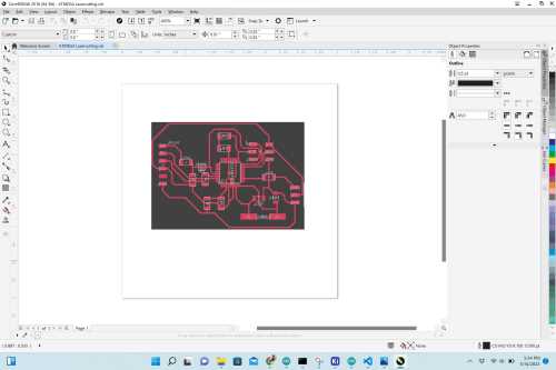
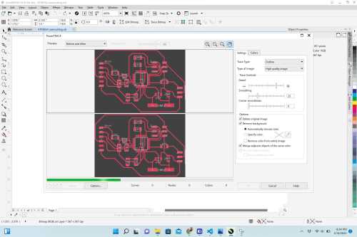
So I grabbed a small scrap of 1/4” clear acrylic and decided to “design” it for rastering. I opened Corel Draw and made my page dimensions 3” x 3”. I took a screenshot of the PCB of the ATMega 328 PCB.
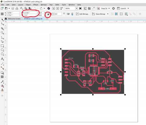
To make sure the size of the rasterd PCB is the same as the size of the actual PCB, I used callipers to measure the width and height between outermost traces (which were 2.1” x 1.5”). I placed the screenshot in Corel Draw, and locked the dimensioning button. Once locked, I changed the height of the png to 1.5”.
Once the screenshot was sized properly in Corel Draw, I traced a bitmap of it.
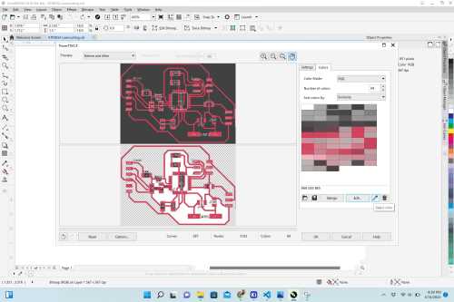
I clicked on the “Colors” tab and removed as much of the gray color as I could.
 |
 |
|---|---|
| The majority of the gray background was removed during the original bitmapping. | There was still portions of dark gray and light gray (writing) that could not be removed during bitmapping. Now I was going to try to remove it all individually. |
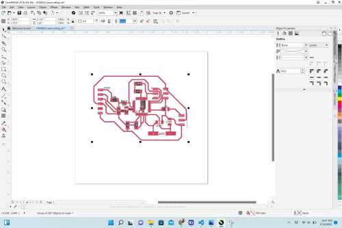
Unsure of how to remove more gray, I decided to ungroup the entire bitmap.
 |
 |
|---|---|
| I was able to select individual groups of gray and then delete it. | The only issue was that if the gray areas overlapped any of the red areas, and I deleted it, it also deleted the red. This caused the future metal tracings to be broken. |
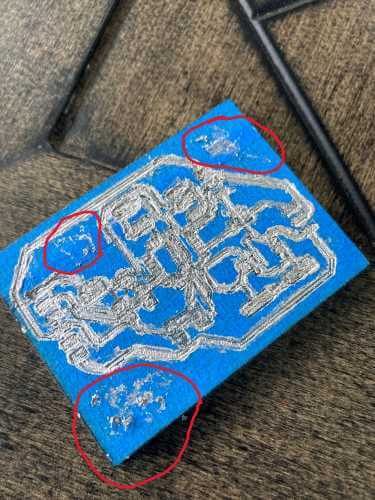
Feeling like I had done all I could do, I decided to simply do a test cut and see how it would look at this point. I covered the 3” x 3” area I intended to use on the 1/4” acrylic with blue painter’s tape on both sides of the acrylic. (I did this to prevent both burn marks and smoke marks while laser cutting. Using the Charlotte Latin School (large Fusion Pro– which has cameras in it), I rastered two ATMega 328 PCB’s. (After all, I do everything in twos.)
 |
 |
|---|---|
| This is what the whole thing looked like after the laser cutting was done. | Interestingly, the areas where the legs of the ATMega 328 chip would need to be soldered was “melded” together (just as I feared). |
I still wanted to see what the circuit tracing would look like if I continued with my plan to “paint” the rastered areas with the metallic pen.
 |
 |
|---|---|
| I used the silver ink pen and filled in all of the areas that had been rastered. It was somewhat difficult to get the ink to fully fill the indentations, and it took about two passes with the pen to fully fill it. | The areas I was concerned about under the chip is indeed not going to work. I am going to need to use another technique to make this work properly. |
I was able to peel the majority of the blue tape off, but some of the areas required me to use a very fine set of tweezers to get it all out.
This is what it looked like when I pulled as much of the blue tape off as I could.
 |
 |
|---|---|
| This view is of the painted side down. If I can get the circuits to work like this, I would like to have the painted side facing down or possible sandwiched between two pieces of 1/4” acrylic. The picture does not do it justice. The trace lines are actually pretty under the “glassy” material. | With the paint side up, the circuit is not as pretty, and you can see the flaws in the paint. Placing another piece of 1/4” acrylic may make it look better. The next step is to determine a way to get the traces and pads more clearly defined. |
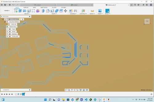
In thinking about how to make the pads (expecially those under the chips) have more definition, I wanted to try a couple of new things. I do feel that bitmaps of the circuits from KiCAD PCB generator may not be the best. I am thinking I need to draw out the circuits in Corel Draw using component measurements.
Idea 1: I wondered if I could get more definition if I used a vinyl cutter and cut out the traces and the component pads. Then, I could use the silver ink pen to fill it in. To test this out, I tried to see if the silver ink would even adhere to smooth acrylic. After much effort, it did not. I wondered if I could use tin and solder paste Sn63/Pb37 No Clean Solder Paste on top of the silver ink.
Idea 2: In the same line as using the vinyl cutter to make a template, I was thinking I could 3D print a very thin template. Then, I could use the silver ink pen and trace the circuit. This would require the acrylic to have texture on it before attempting to trace it. One thing that I could do is to raster the surface of the acrylic and then use the silver ink pen on the textured surface.
Any idea moving forward was going to require me to draw the circutis. I decided to use callipers and meausre the physical pads for all of the components and draw the circuits in Corel Draw.
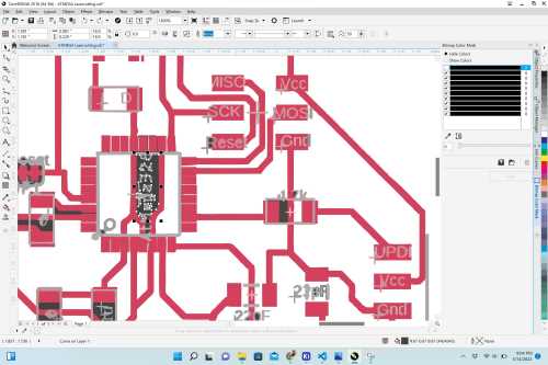
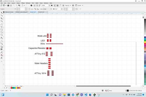
I began a new drawing in Corel Draw. I had an old unstuffed ATTiny 412 MVP PCB and a good pair of callipers. This particular PCB had an ATTiny 412 chip. a capacitor, a resistor, an LED, and three male headers on it. One other component that I wanted to include in a new circuit drawing was an RGB LED. The pad for the RGB LED was a little tough because I didn’t have have an unstuffed PCB with an RGB LED on it. I used the callipers and measured the metal pins on the under-side of the RGB LED and add the horizontal and vertical spaces between them.
The tools in Corel Draw that proved to be very important in designing the pads for the components are shown below.
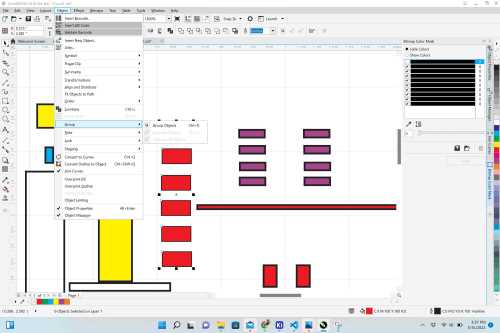
By unlocked the horizontal and vertical dimensions, I was able to enter exact measurements to obtain rectangles that were closer to the actual size. I also heavily relied on the the X and Y positions. Thes aided me in lining up the pads when needed– especially the pads on the ATTiny 412 and ATTiny 1614 chips and the the pads on the RGB LED.
 |
 |
|---|---|
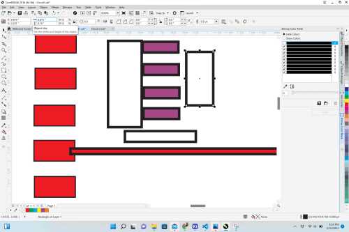
| After measuring the dimensions of the components’ pads, I used a series of rectangles that I could fill (and eventually raster). I also used the rectangles as measurement tools. Once a component’s pad was complete, or I connected it to another component, I filled the rectangle with red fill. | It was important that I group the components as I completed them. This allowed me to move the whole component’s pads easily. |
I eventually completed designs for all of the components.
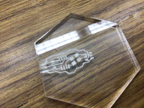
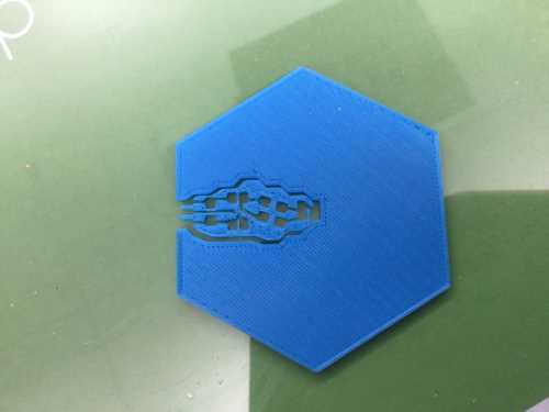
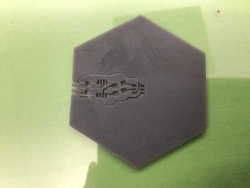
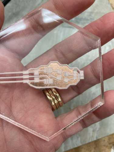
With the design in Corel Draw complete, I decided to try it out on the laser cutter. I first did a test cut of the circuit design on cardboard. One of my students (LJ) created a digital “Settlers of Catan” game last semester, and she had several hexagons with a diameter of 2.5” cut out of 1/4” acrylic. I wanted to use the acrylic hexagons for my “simple circuit”. The following video shows my test cut and first cut on acrylic.
This is what the acrylic hexagon looked like when it was finished.
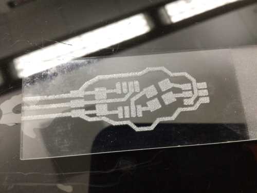
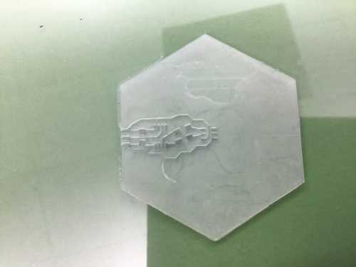
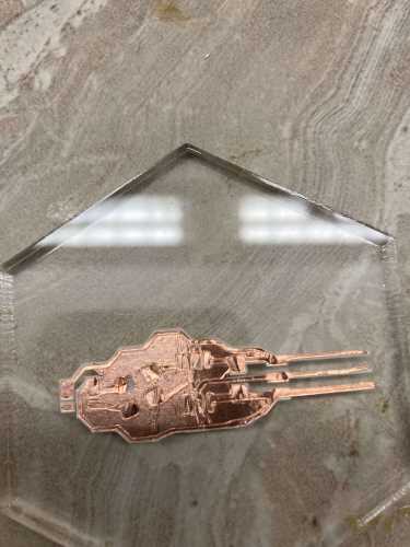
I had obtained a few glass microscope slides from the biology department at Charlotte Latin School, and I wanted to see how my circuit design would cut on them. The following video shows two successful rasters of my design on glass.
This is what the design looked like after being cut on glass.
 |
 |
 |
|---|---|---|
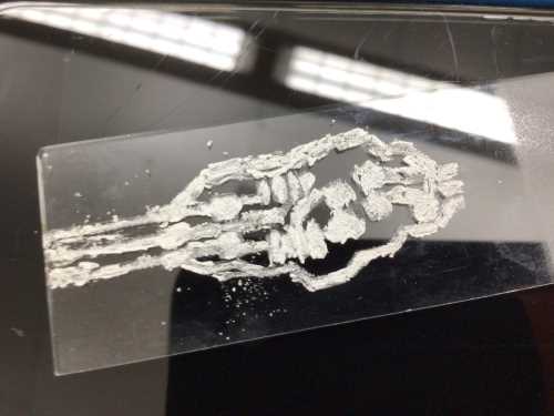
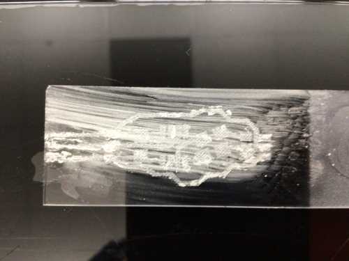
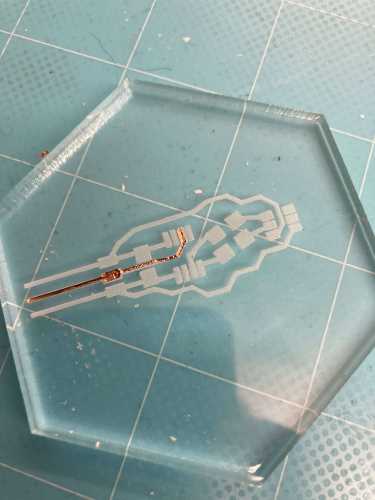
| Just after it was rastered on the laser cutter. | I used the silver paint and filled in the areas that had been etched by the laser cutter. | I went to wipe away the sloppy metal infill, and it smeared terribly. |
As I continued to laser cut the design on the glass microscope slides, I realized the glass was not very strong. This video shows two glass slides breaking in half as they were laser cut.
I finally realized that the glass microscopes slides were breaking when there was nothing under it in the bed of the laseer cutter. If the micrsocope slide was placed on a piece of cardboard first, it did not break. I wanted to get the rastered image as deeply cut into the glass as possible, and I ran the job three times.
At this point, I really wanted to try something else. The following table shows everything I tried.
| Image | Description |
|---|---|
 |
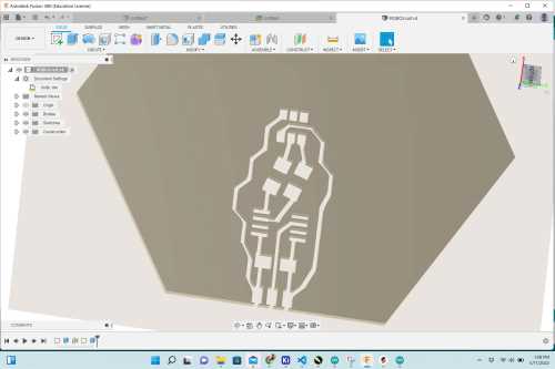
I decided to try my hand using 3D printing to design this circuit. In my thinking, I was hoping to make a “stencil” of sorts and “stuff” it with metal. So I began making a 3D version of the circuit in Fusion 360. The first thing I did was make a hexagon (the same sizw as the acrylic scraps I had been using). I extruded the hexagon 1.5mm, and placed an offset plane on the top of it. On the offset plane, I then imported a screenshot of the circuit. |
 |
I had to remove the insternal lines within the image I placed on the offset plane. This was a dauting task as there were many of them, and it often took two attempts to eliminate them. |
 |
I deleted the internal lines on the offset plane. |
 |
I continued to delete the internal lines on the offset plane. |
 |
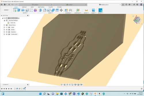
Once all of the internal lines were completely deleted, I was able to extrude the outlined image -2mm. This made a cut in the hexagon, and the .stl was created. |
 |
This is just another view of the .stl I created. |
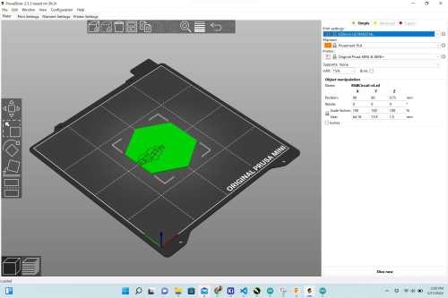 |
This is the .stl file in Prusa Slicer as I was obtaining the gCode for 3D printing. |
 |
This what the design looked like as it was printed on the Prusa Mini 3D Printer at the CLS Fab Lab. I had plans to fill the internal structure with metal. I found some copper tape that was 1/4” wide, and I wanted to use it to line the inside of this design. |
 |
I printed the design on the Form 3S Printer at CLS Fab Lab with Tough 2000 resin. |
 |
I also 3D printed the deisng on the other Form 3S Printer at the CLS Fab Lab suing Durable resin. I wound up not attempting to use either of these as I felt the copper would not adhere properly in the channels. |
 |
I used the 1/4” copper tape and tried to make a solid square out of it. I then used the vinyl cutter at the Charlotte Latin School Fab Lab to try to cut a solid circuit out of it. When I traced the bitmap of it in Silhouette Studio, I did not reduce the size of it. I had planned to reduce it after seeing how the first attempt went. This did not prove to be a good experiment because the copper tape strips did not stay together. I decided to order 2” copper tape to test this later. At that time, I also ordered low-temperature solder paste (with the hope of testing again on acrylic or glass). |
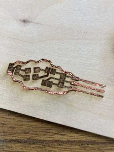 |
While waiting for the two new materials to arrive, I decided to do some tests on wood using the laser cutter in the Charlotte Latin School Fab Lab. This first circuit on wood was on a scrap piece of wood with lower density. I used the deep engrave setting, and afterward began using the `/4” copper tape to line and stuff the rastered channels. As I did this, some of the wood “walls” that were between some of the component pads began to break. |
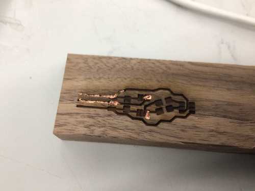 |
After using lower-density wood, I rastered the circuit on the CLS laser cutter– again using the deep engrave setting. This time, I used very dense, hardwood– walnut. |
 |
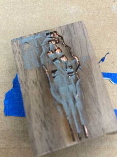
I began lining/stuffing the walnut-engraved circuit with the 1/4” copper tape. This time, Tom Dubick suggested that I use a miltimeter to see if I was getting conductivity by doing this. I checked, and it did seem to be working. I continued to pack the channels in the wood with copper tape. |
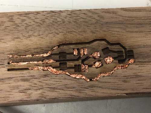
 |
This shows the wood circuit completely packed with copper tape, and I was ready to solder components onto it. |
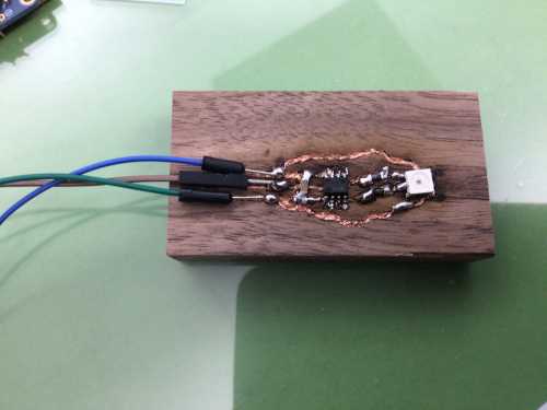 |
This was a really bad idea. Trying to solder components onto this did not work at all. The heat from the soldering iron (around 750 degrees F) burned the wood and actually liquified the resin inside the wood. While I was able to get the components soldered on and secure, I could never upload code to it. I couldn’t even get enough power to it. |
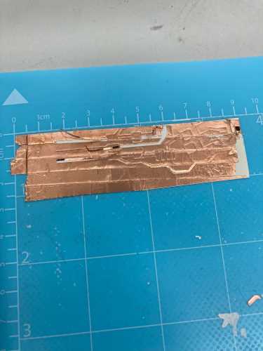
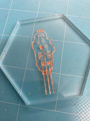
| The 2” copper tape arrived at the Charlotte Latin School Fab Lab, and I used it to create a “sticker” of the circuit using the vinyl cutter. This time, I measured the outer hosizontal parts of the circuit (1.91”), and I sized the “sticker” accordingly. | |
 |
I transferred the copper circuit onto a rastered acrylic circuit. It was difficult to remove the copper from outside of the circuit’s traces. I knew this was going to take a lot of practice and very steady hands getting this to work. |
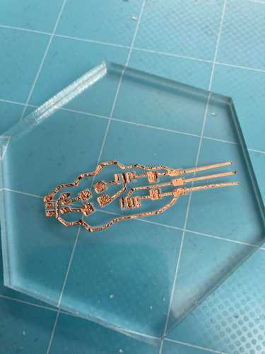
 |
This image shows the other side of the circuit above. I was really impressed with how pretty the copper looked in the shiny acrylic. I definitely wanted to keep trying to use this 2” copper tape. |
 |
I decided to raster another circuit onto the acrylic and gently place the copper pads and traces onto the corresponding areas. |
 |
I continued to add copper to the rastered circuit. |
 |
This shows one rastered acrylic circuit completely covered with copper traces that were cut using the vinyl cutter. |
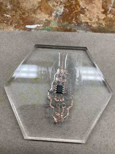 |
I then soldered the ATTiny 412 chip onto the circuit. |
 |
I soldered the RGB LED and the capacitor onto the circut. The low-temperature solder paste was actually working very nicely. The soldering iron was heated to 378 degrees F. |
 |
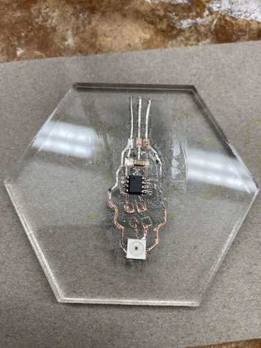
This is the completely soldered circuit. Instead of soldering male headers onto the VCC, UPDI and GND copper pads, I soldered male-male wires. This was a huge mistake as they kept pulling the copper traces up. |
| This video shows me trying to upload the RGB code to the ATYTiny 1614 chip. | |
 |
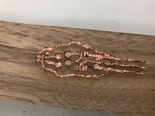
With the low-temperature solder paste working seemingly well on the last circuit, I wondered if I could make it work with the circuit rastered into walnut. I cut the circuit pads and traces on on the 2” copper traces and peeled and placed it into the channels in the wood. I then began to add solder to the circuit. |
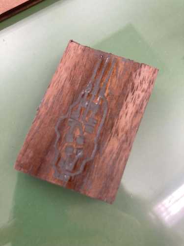 |
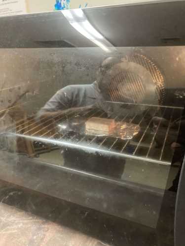
I completely jammed low-temperature solder into the wood channels (with the copper pads and traces) and scraped the surface clean. After a conversation with Charlotte Latin Art teacher and Fab Academy graduate– Richard Fletcher– I decided to put the walnut/low-temperature solder into the convection oven at ~380 degrees F. |
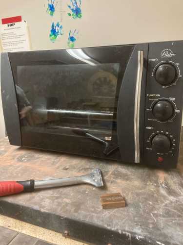 |
This is the convection oven that I used in the Charlotte Latin School art department. It was very difficult to get the solder paste to “meld”– even as I increased the temperature and time in the convection oven. |
 |
This is the circuit with low-temperature solder paste sitting on a piece of aluminum foil in the art department’s convection oven. |
 |
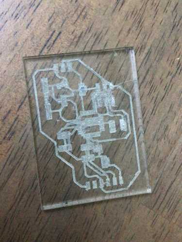
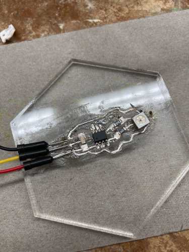
I am finally getting somewhere with these materials. I used a glass microscope slide, and adheared a vinyl-cut sticker (out of the 2” copper tape) of the copper pads and traces onto the clean surface. This is the cleanest version of the circuit that I had made to this point.} |
 |
The components easily soldered onto the glass slide, and the male headers were a huge improvement. I was able to upload the RGB code (used in previous electronics weeks), but the RGB LED never lit up. |
| This video shows me successfuly uploading the RGB code to the circuit on the glass microscope slide. |
Very confused as to why my RGB circuit was not working, I feel that I was not using the same RGB LED’s that I had used before. Midway in Fab Academy, Tom Dubick ordered more RGB LED’s, and I do not think I have the correct data sheet (and orientation) of the RGB LED. I decided to take a step back from the RGB LED and return to Tom Dubick’s MVP circuit.
| Image | Description |
|---|---|
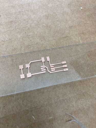
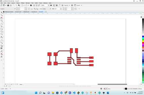 |
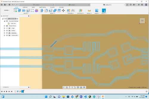
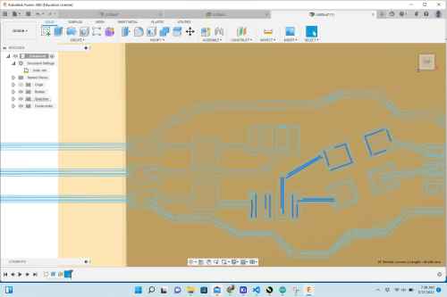
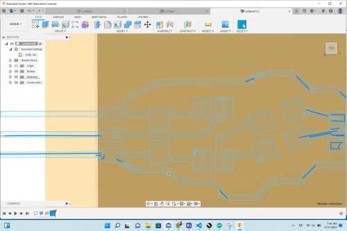
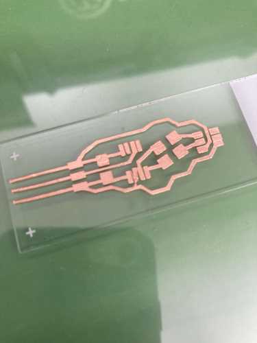
I designed Tom Dubick’s MVP circuit using Corel Draw. I used the footprints I had designed for different components when making the RGB Circuit. |
|
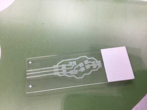
I took a screenshot of the MVP circuit when I had it completed and measured it’s size to be ~1.20” horizontally.) |
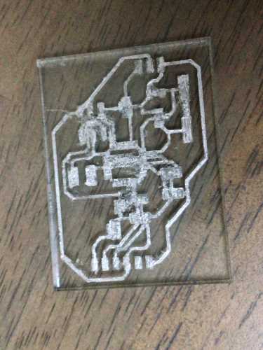
 |
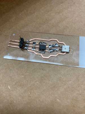
I cut the copper traces of the MVP circuit on the CLS Vinyl Cutter, and tediously placed it onto the glass microscope slide. |
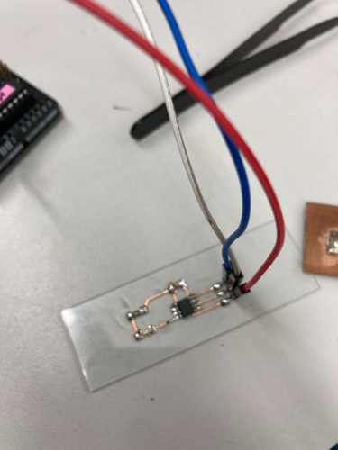 |
This is what the MVP cicuit looked like after I had soldered all of the components onto the copper “sticker”. This photo was taken just before I tested it with the Blink Code in Arduino. |
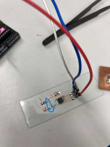 |
The circled area in the circuit is where I inadvertently had a copper trace. This copper trace was preventing the LED from blinking at first (as shown in the video below). |
The following video shows my “hero shot” with a fully functioning MVP circuit on glass.