Week 17 Assignment: Magical Lantern Carousel Ring PCB and PCB Compartment Design and Manufacturing
Project Background
This week, I dedicated most of my time to an important component of my Fab Academy 2025 final project — the design and manufacturing of the magical lantern carousel controller board. In Week 16, I conducted system design and modified the hardware solution. By Week 17, I needed to design a completely new ring-shaped PCB (suitable for placement on top of the lantern's circular gearbox) to control the entire system, including the lantern's rotation mechanism, LED lighting effects, and gesture interaction functionality. This design process was largely completed through communication with Claude, under AI guidance (of course, drawing schematics and routing still had to be done by myself). After completing the PCB design, I also exported the PCB model from LCEDA (JLC EDA) and finished designing the PCB compartment structure in Fusion 360.

The PCB for the magical lantern is planned to be placed on top of the circular gearbox
Design Requirements Analysis
After several weeks of experimentation, I finally figured out what functionality this PCB needs:
- Shape Requirements: Must be ring-shaped, with an outer diameter of 92mm and inner diameter of 22mm as estimated in Fusion 360, as it needs to fit on top of the lantern's circular gearbox.
- Core Control MCU: Using Seeed Studio's XIAO ESP32C3, which is compact, has Wi-Fi, and offers sufficient functionality.
- Sensing System: Connecting 3 APDS-9960 gesture sensors to ensure 360° coverage for receiving gesture commands without blind spots.
- Lighting and Power: Controlling 2 strips of RGB LED strips with 14 LEDs each, and 1 motor driven by a Grove mini fan motor driver.
- Power Management: Preferably with automatic switching between battery and USB, which is crucial.
- Future Expansion: Bringing out unused pins and reserving several Grove interfaces for potential future functionality.
- Manufacturing Process: This time a double-layer board is necessary, as a single layer cannot satisfy my ambitions.
Communicating with AI to Design the PCB
First, I provided Claude with what I believed to be as detailed project background information as possible, including basic appearance rules, key design requirements, APDS-9960 gesture sensor reference materials, background information on the magical lantern carousel, current project progress with resolved and unresolved issues, the XIAO ESP32C3 pin diagram, and parameter table screenshots from the LED strip purchase website. Then I asked Claude to guide me in drawing schematics and designing the PCB using KiCad.

Providing Claude with as much detailed background information as possible to guide me in using KiCad to draw schematics and design the PCB
Since the communication process contains a large amount of information, you can access the shared dialogue link.
https://claude.ai/share/430d4652-be82-4899-aa72-39eb7a691ac2
The content below is organized based on the final completed design and manufacturing process. I rewrote it based on the initial draft provided by AI, combined with the actual situation.
The Struggle with Design Tools
Initially, I used KiCad to draw schematics, but eventually switched to LCEDA (JLC EDA). Why? There were several reasons:
- The interface is extremely user-friendly for Chinese users like me.
- Their component library is super rich and comes with 3D models, eliminating the need to find them yourself.
- The best part is being able to order components directly from the BOM table, saving the hassle of hunting for parts elsewhere.
- Design can be sent directly to the manufacturer, providing a seamless service.
- LCEDA Professional is free and offers an online version, requiring no software installation; the entire process from design to manufacturing can be done in a browser.
To be honest, migrating from KiCad to LCEDA wasn't entirely smooth, but it was worth it for the later convenience. And once you become familiar with schematic and PCB design, the specific tool gradually becomes less important.
| Comparison Item | KiCad | LCEDA |
|---|---|---|
| Open Source | Completely open source | Closed platform |
| Learning Curve | Steeper learning curve | Beginner-friendly |
| Component Library | Need to find/create yourself | Rich with 3D models |
| Chinese Support | Available but not perfect | Native support |
| Manufacturing Integration | Need to export Gerber | One-click production order |
| Component Procurement | Processed separately | Order directly from BOM |

Schematic initially drawn using KiCad

Schematic drawn using LCEDA, the entire process was done in the browser
Schematic Design Process
Core Module Design
When drawing the schematic, I first had to figure out the power system:
Battery ----> Diode ----> Switch ----> V_BATT_PROTECTED Circuit
USB 5V ----> Diode ----> V_BATT_PROTECTED CircuitThis may look simple, but there's a lot of science behind it. Claude suggested I use a 1N5822 Schottky diode instead of a regular diode because of its low voltage drop (only about 0.4V), meaning less energy would be wasted. This is a great power-saving approach for battery-powered devices!
Additionally, under AI's recommendation, I added two capacitors: a 10μF electrolytic capacitor and a 0.1μF ceramic capacitor. These two capacitors work like a combination of a power "reservoir" and "filter" — the large-capacity electrolytic capacitor handles low-frequency noise, while the small-capacity ceramic capacitor takes care of high-frequency noise. Without them, various inexplicable problems could occur in the circuit.

Figure 3: Power management circuit schematic
Grove Interface Connection Scheme
I planned to bring out the extra pins through Grove interfaces, but the wiring was a question. Initially, AI gave a Grove interface pin arrangement of VCC-GND-SIG1-SIG2, but after researching Grove for Beginners' Grove interface, I discovered the actual sequence is SIG1-SIG2-VCC-GND! I almost connected it incorrectly. AI can easily make mistakes in details, especially in areas where background information hasn't been explicitly provided, so extra caution is necessary.

I provided Claude with a reference image of a board full of Grove interfaces
Output Control Interface
The LED strip uses the WS2812B chip, also known as "smart RGB LED with integrated driver IC." This device only requires a single data line to control the color of a long string of LEDs, eliminating a lot of wiring hassles.
Fun fact: The WS2812B communication protocol is a single-wire return-to-zero code with strict timing requirements. Each LED receives 24 bits of data (8 bits each for RGB) and then passes the remaining signal to the next LED, enabling cascade control.
PCB Layout Design - An Interesting Turn
Originally, I planned to make a perfect ring-shaped PCB, as shown below, to be placed on top of the gearbox.

But when I received the battery, I discovered this big guy wouldn't fit in! I created a placeholder model in Fusion 360 using the battery's dimensions (the red part in the image below), tried different arrangements for half a day, and found that the best approach was to fully utilize half of the gearbox space, as shown below.

Making full use of half the gearbox space proved to be the best placement solution
I made a last-minute decision to cut off a piece of the ring to make room for the battery. Following this idea, I designed a top cover for the gearbox that would also serve as a support structure for the PCB, with holes to facilitate wiring and reduce material usage. The effect in Fusion 360 is shown below.

Added a circular cover missing a piece to the gearbox which also serves as a support structure for the PCB
This is why the PCB design looks like a "mooncake with a bite taken out." I arranged the components as reasonably as I could based on my understanding.

3D effect of PCB layout
When laying out, I followed several principles:
- Place XIAO ESP32C3 at the top for easy access to the programming interface
- Distribute the three gesture sensor interfaces as evenly as possible to cover different directions
- Keep power management components together to avoid interference with other circuits
Speaking of layout, here's a practical tip: place large components first, then smaller ones. First determine the positions of components that are location-constrained or fixed (such as connectors, large components), then arrange the more flexible small components (like resistors, capacitors).
Routing Strategy - The Secret of Double-Layer Boards
This time I tried a double-layer board, which offers much more freedom compared to a single-layer board. My routing strategy was:
- Top Layer: Mainly for power lines and important signal lines, using thick 1.0mm traces for power
- Bottom Layer: Most of it made into a GND plane, providing a low-impedance ground path
- Vias: Appropriately added vias connecting the top layer GND to the bottom layer ground plane
Personal insights on routing:
"Don't underestimate the job of routing; there seem to be many techniques! It's best to bend traces at 45° angles, not 90° right angles; signal lines should not run parallel for too long, or they might interfere with each other; high-speed signals should be short and direct; always add sufficient decoupling capacitors between power and ground. These small details determine whether the board will be stable and reliable when manufactured."
Routing was probably the most time-consuming process in my PCB design, with many details requiring multiple attempts to find the right solution. 
The final completed PCB board design, I added some support mounting holes

3D rendering of the completed PCB board design
LCEDA also allows exporting 3D models as obj files, as shown below.
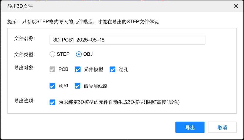
Option to export OBJ models in the Export 3D File dialog
In Fusion 360, I can import OBJ files through the design interface's Insert/Insert Mesh, allowing me to see the actual 3D effect of the PCB part in my design.

Importing the PCB model into the current structure helps evaluate the PCB and structure
Component Selection and Ordering - Taobao Engineer Online
As a seasoned "Taobao engineer," component procurement has now become my "strength." Here are some of my choices and considerations:
Schottky Diode (1N5822)
This unassuming component is actually very important. I chose it because:
- Low forward voltage drop, only about 0.4V, much more power-efficient than regular diodes at 0.7V
- 3A current capacity, far exceeding my system's 0.5A requirement, providing sufficient margin
- Fast response speed, suitable for protection circuits
Capacitor Selection
I deliberated for a long time on capacitor selection:
- Electrolytic capacitors need low ESR (equivalent series resistance) for better filtering effect
- Chose Y5V dielectric for ceramic capacitors, which, although less stable than X7R, is cheaper and basically sufficient
Connectors
- Used JST-SH compatible 1.0T-4P surface mount connectors, these small and delicate connectors are perfect for gesture sensors
- Used more common PH2.0 series interfaces for LED strips and Grove interfaces
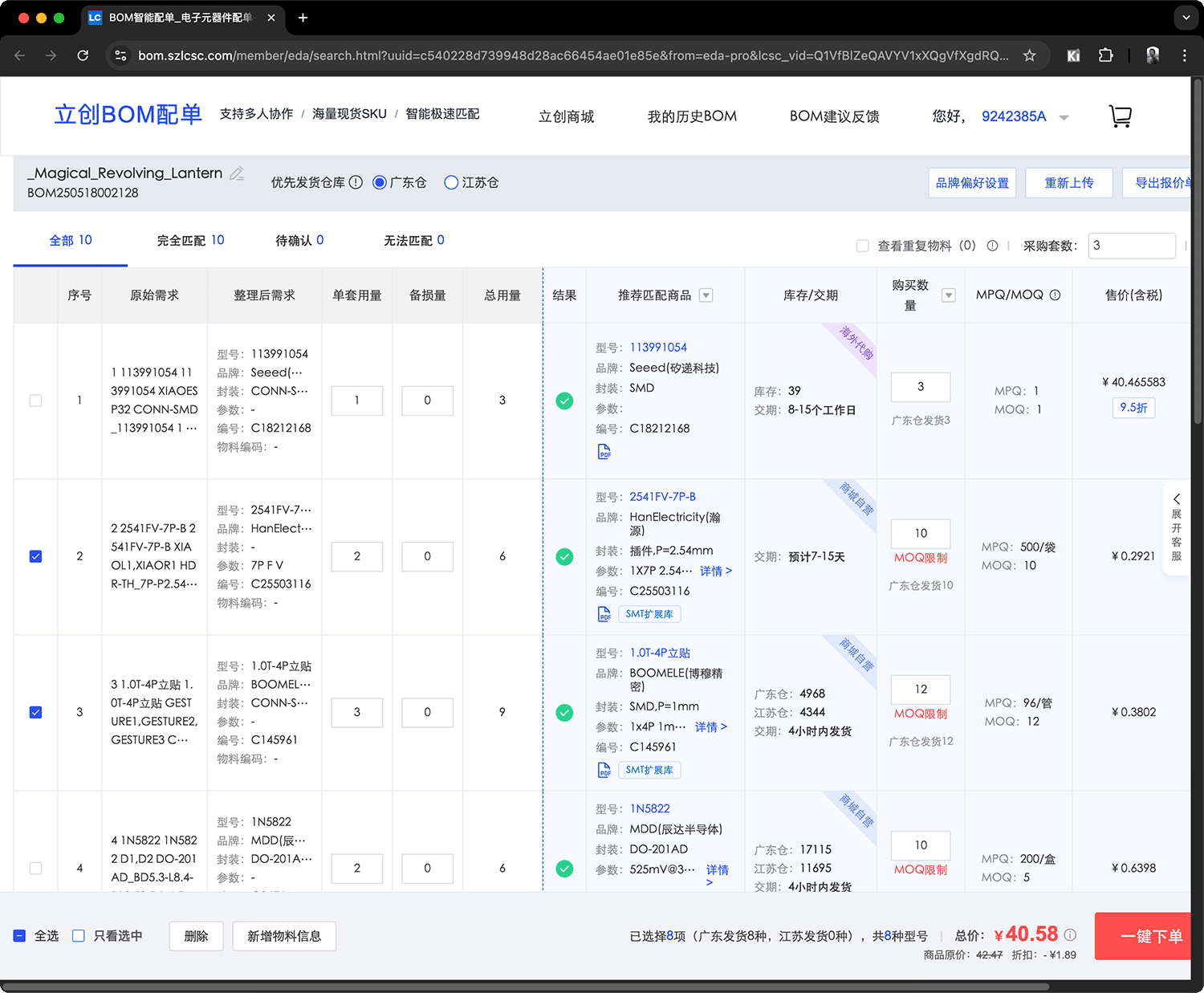
Exporting BOM Table
When exporting the BOM table in LCEDA, it provides a "Component Order" function, as shown below.

Location of the "Component Order" function button when exporting BOM in LCEDA
Next, I could select the procurement quantity. I planned to procure 3 sets (if time permits, I want to make 3 lanterns).

Directly input the procurement quantity; since I don't have much knowledge about component brands yet, I didn't expand the selection
On the BOM ordering page, I could select which materials I needed. I excluded the XIAO ESP32C3 and Grove interfaces (which I already had).
All the needed components cost only 32.13 yuan in total! With free shipping! I chose shipping from the Guangdong warehouse, and the components arrived the next day, which was impressively efficient. In the order below, all quantities were ordered according to the minimum order quantity.
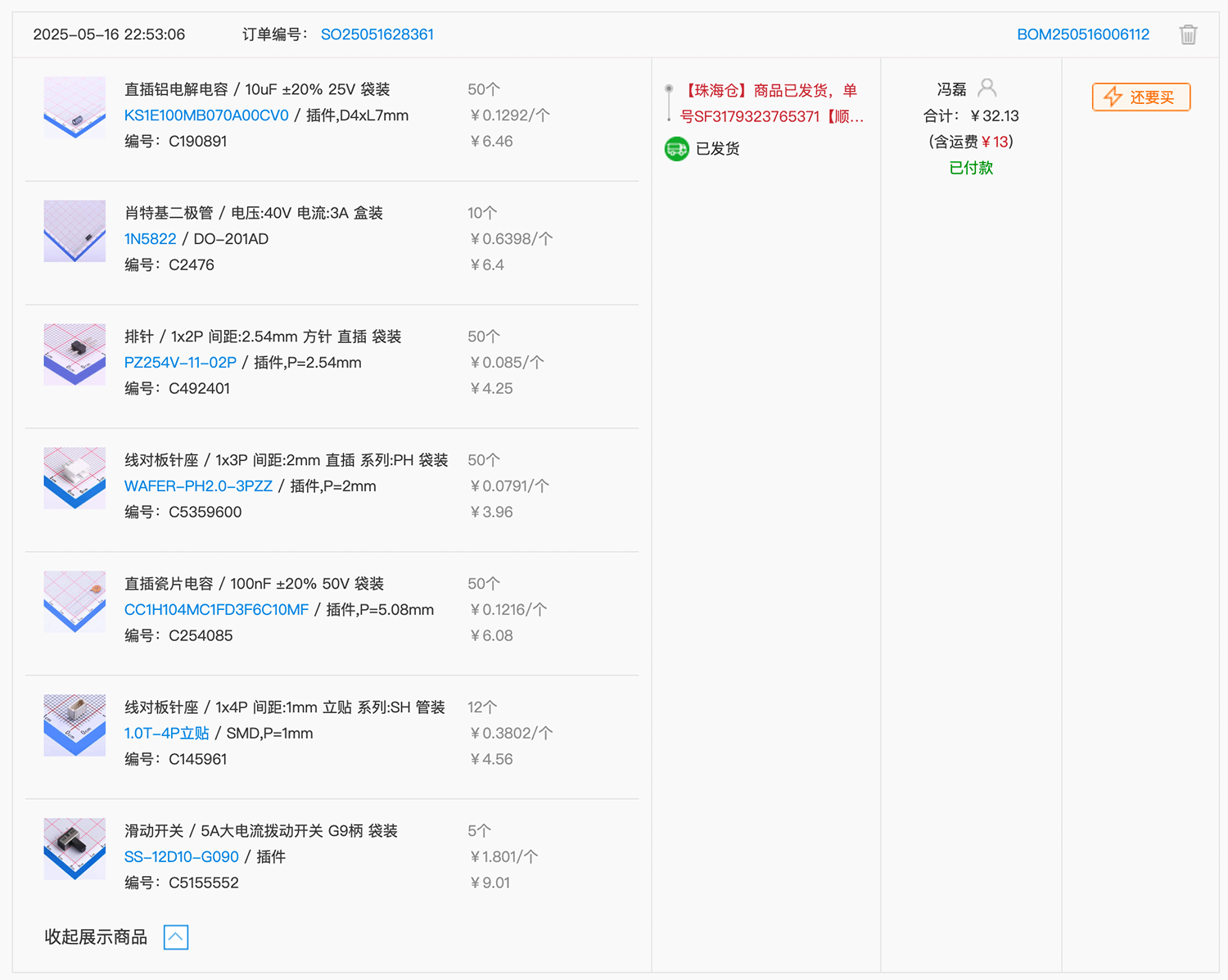
Figure 6: Screenshot of component order


The received components were packaged in separate bags, poured out for inspection and photography
PCB Manufacturing - An Unexpected Surprise
When submitting the PCB manufacturing order, there was an unexpected surprise. This double-layer board was even cheaper than the single-layer board I had made before! I got 5 PCBs for just 33 yuan.
After careful investigation, I discovered that in my first version, I had selected "lead-free hot air leveling," a non-standard process. This time I chose the ordinary "leaded hot air leveling," which was much cheaper.
Manufacturing process tip: Ordinary leaded hot air leveling can fully meet personal project requirements at a lower cost. Lead-free processes are mainly to meet environmental protection requirements, which may not be a primary consideration for small-batch manufacturing in the prototype development stage.
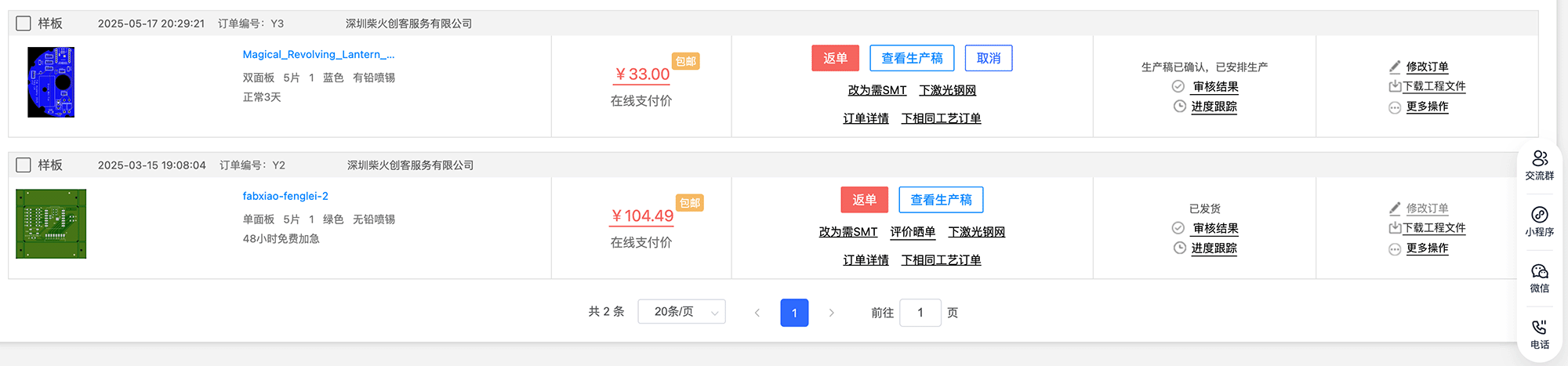
Screenshot of PCB manufacturing order
Remaining Structural Design
This part took more than a day. I gradually completed the design of the PCB compartment and gesture sensor brackets in Fusion 360, then 3D printed the structures for testing.

Gradually completed the design of the PCB compartment and gesture sensor brackets in Fusion 360
I 3D printed the PCB compartment and gesture sensor brackets. The 3 main structures can be connected firmly together just through nesting.

After 3D printing, the 3 structural compartments can be firmly connected together through nesting. When combined with the outer frame and rotation mechanism, the entire structural main part work is completed
Now I'm just waiting for the PCB.
Challenges Encountered and Solutions
To be honest, this process wasn't entirely smooth; I encountered several challenges:
- Inadequate Current Estimation
- Problem: Underestimated the current requirements of the LED strip
- Solution: Recalculated the maximum current when fully lit (about 0.5A), selected diodes and switches with larger capacity
- Spatial Layout Challenges
- Problem: Battery too large, standard ring wouldn't fit
- Solution: Modified PCB shape, cut off a portion to make room for the battery
My experience is: don't panic when encountering problems, analyze carefully first, and communicate fully with AI by providing comprehensive background information to get valuable guidance.
Some Personal Insights and Recommendations
As a PCB design novice, this project taught me quite a bit. Here are a few insights to share:
- Tools aren't important; understanding basic principles is
- Whether using KiCad or LCEDA, circuit principles are universal
- Double-layer boards are so much better than single-layer boards
- More flexible routing, better signal quality, strongly recommend beginners start directly with double-layer boards
- The domestic tool and service ecosystem is already very mature
- LCEDA + JLC manufacturing + JLCSMT electronic components, this one-stop service is really excellent
- Hands-on experience beats theoretical knowledge
- No amount of theoretical knowledge compares to designing a board yourself and solving problems as they arise
Future Work Plan
Getting the PCB done is just the first step. Next, I need to:
- Solder all components onto the board
- Write control firmware, test each functional module
- Integrate the PCB into the lantern's mechanical structure
- Conduct overall system testing
- Design and install lantern carousel patches
- Write documentation
I hope in another week, I'll see this magical lantern carousel working perfectly!
PS: Any questions or suggestions, feel free to discuss! All materials for this project will be open-sourced and shared, hopefully helping other makers!