Week 06. Electronics Design
After struggling to work with HTML for 5 weeks now I decided to convert my HTML to MKdocs with Markdown because I realized it is much more time saving and easier to organize the syntax. To learn some basics syntax it is here.
It was not that complex to migrate the whole thing I have done so far but but yes we need to manage some extra time so we can align with weekly assignment.
To do this I firstly downloaded the default template for MKdocs from Julian’s student template Mkdocs and copied all the files to my local folder. In mkdocs.yml file I customized with my personal information. Then I copied html file and edited removing just the html tags.
When I was migrating I copied the images from old folder to and pasted to MKdocs folder without completely removing from html folder and linked to the website. Luckily our Guru Mr. Rico stopped from creating a new folder and pushing to the cloud as my website is going to increase amount of cloud storage requirement. So I cut the entire image, video and design files and pasted to the MKdocs local folder. Then I completely removed the html folder from local folder and did git push. Everything worked well.
KICad
Coming back to week 06 we were introduced with some of the electronics components and the PCB designing softwares. For this week and throughout my FAB academy I will be using KICad for designing PCB as I am already slightly familiar to it compared to other softwares.
- To install KICad go to this link KICad
To add fab library in KICad I followed the steps bellow which is given in the git repo:
- To add fab library clone or download from Fab Library and rename the directory to fab.
- Store it in a safe place such as ~/kicad/libraries or C:/kicad/libraries.
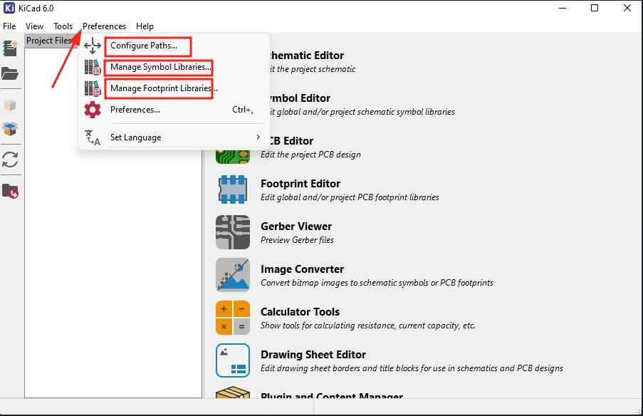
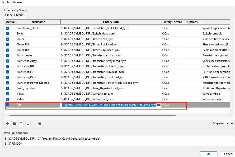
- Open KICad and Go to Preferences >> **Manage Symbol libraries and add fab.kicad_sym as symbol library.
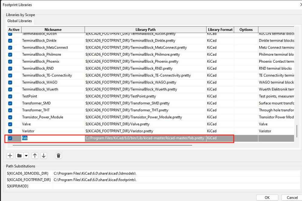
- Go to “Preferences / Manage Footprint Libraries” and add fab.pretty as footprint library.
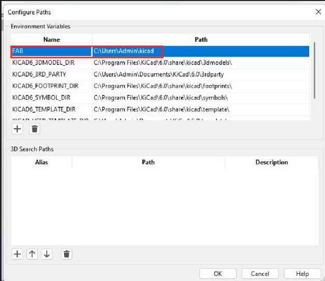
- Go to “Preferences / Configure Paths” and add variable named FAB that points to the installation directory of the fab library, such as ~/kicad/libraries/fab or C:/kicad/libraries/fab. This will enable the custom 3D shapes to be found. The 3D shapes project has just started and most of them have to be populated still.
Assignment
-
Group Assignment:
- Use the test equipment in your lab to observe the operation of the micro-controller in a board.
-
Individual Assignment: - Design a development board to interact and communicate with an embedded micro-controller. - Extra credit: Try another design workflow. - Extra credit: Make a case for it. - Extra credit:Simulate it’s operation.
Link to the group assignment is here
Individual Assignment
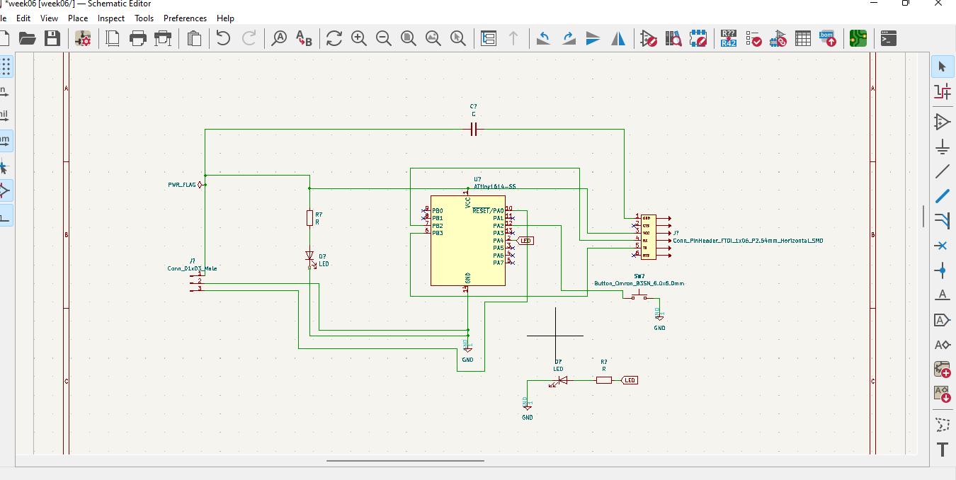
I want to make a programmable board to blink a LED when button is pressed using the component as bellow: 1. micro-controller ATTiny 1614 2. Resistor 1k 3. FTDI 4. 2 LED 5. UPDI 6. Capacitor 7. Push button
Creating Schematic design
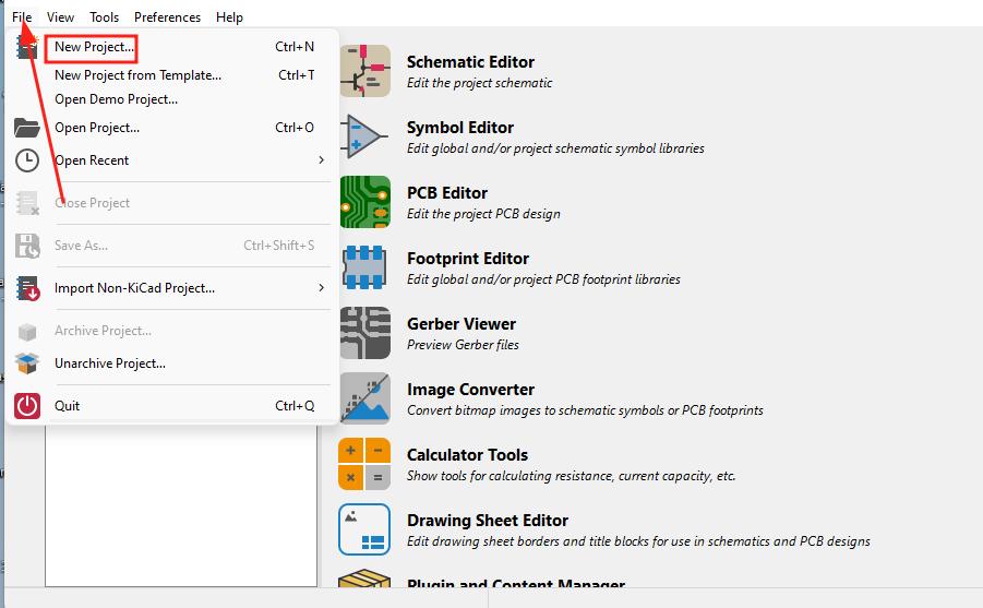
- Firstly open the KICad and under File menu create a New project. I renamed it as week06 assignment.
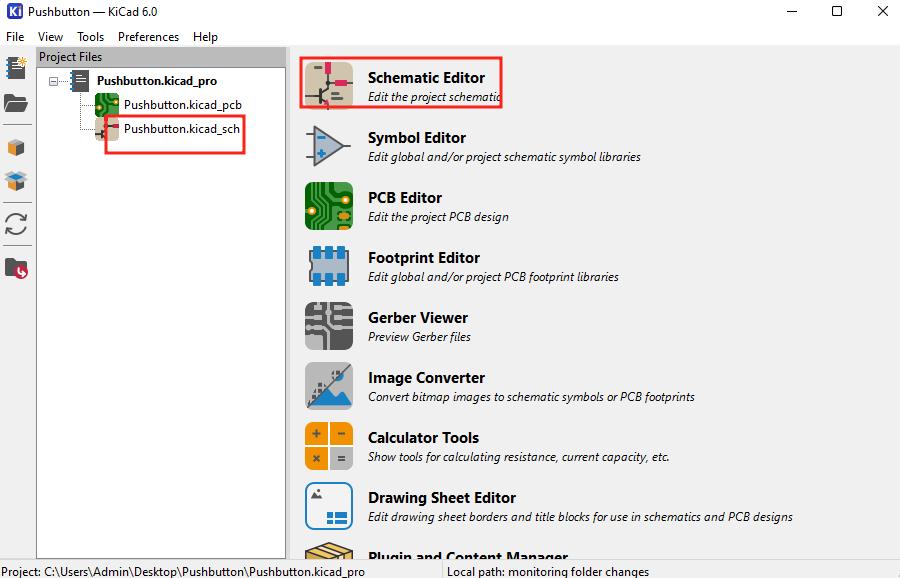
- Click on the Schematic Editor or the _sch file.
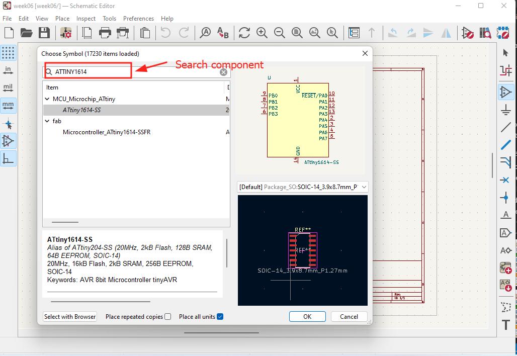
- Use letter A to load the component and place it in the workspace. It type the component name in the search bar to find my component.
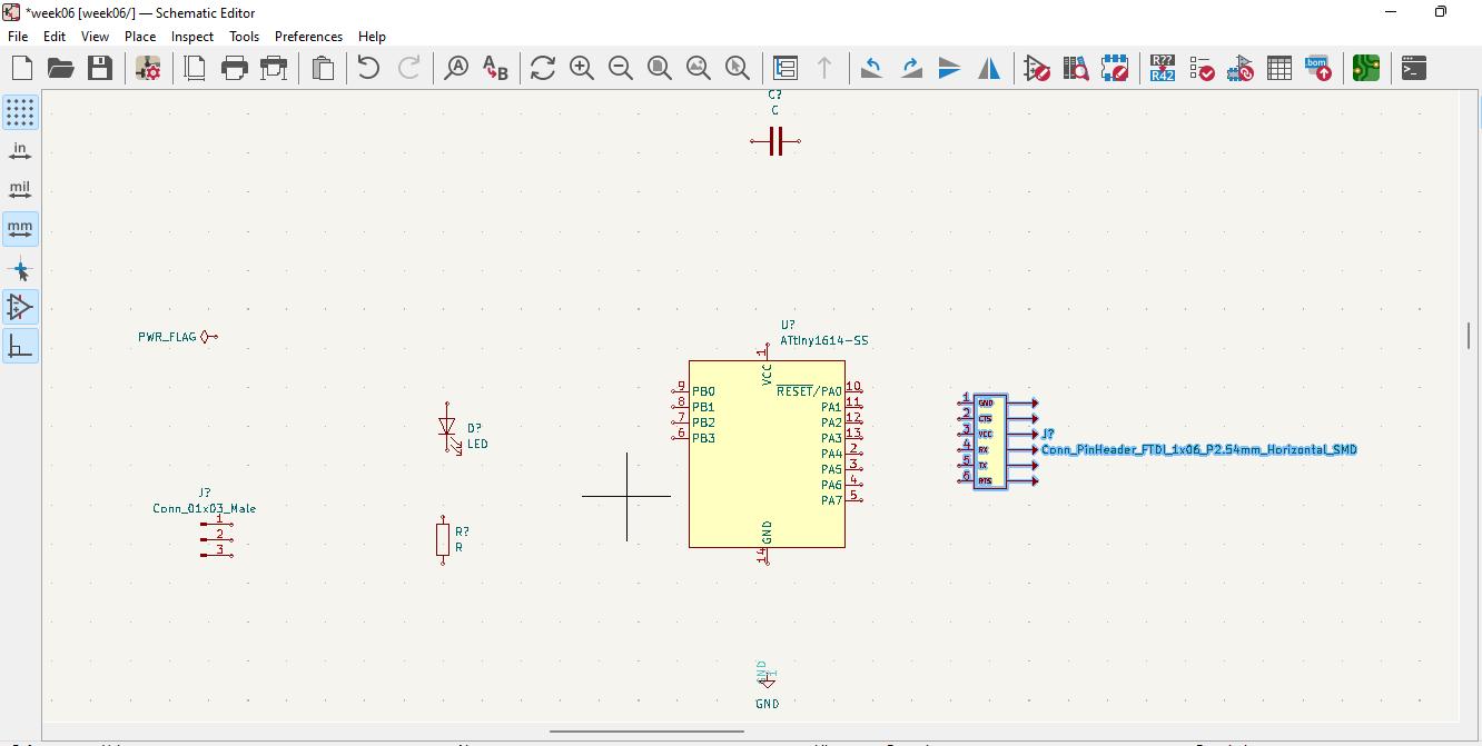
- After placing all the required components on the work space I connected with wire.
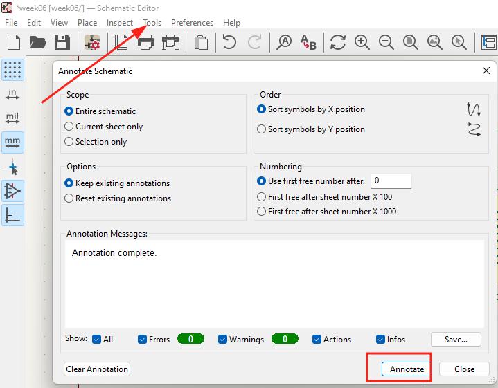
- Before running Electrical Rule Checker I did annotation to the components. Under tool menu choose >> Annotate schematic >> Annotate.
-
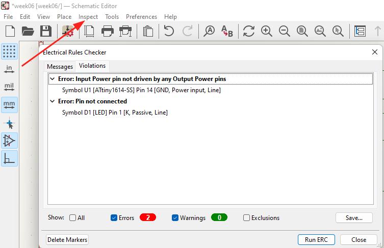
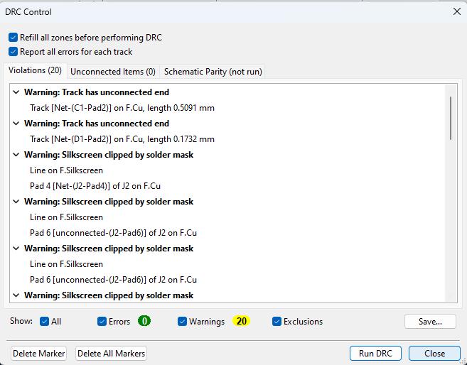
After completing all the component connection I did Electrical Rules Checker (ERC) under inspect menu. I found some errors in connection as shown below.
-
I forgot to give Power flag to GND so I made correction and found 0 error.
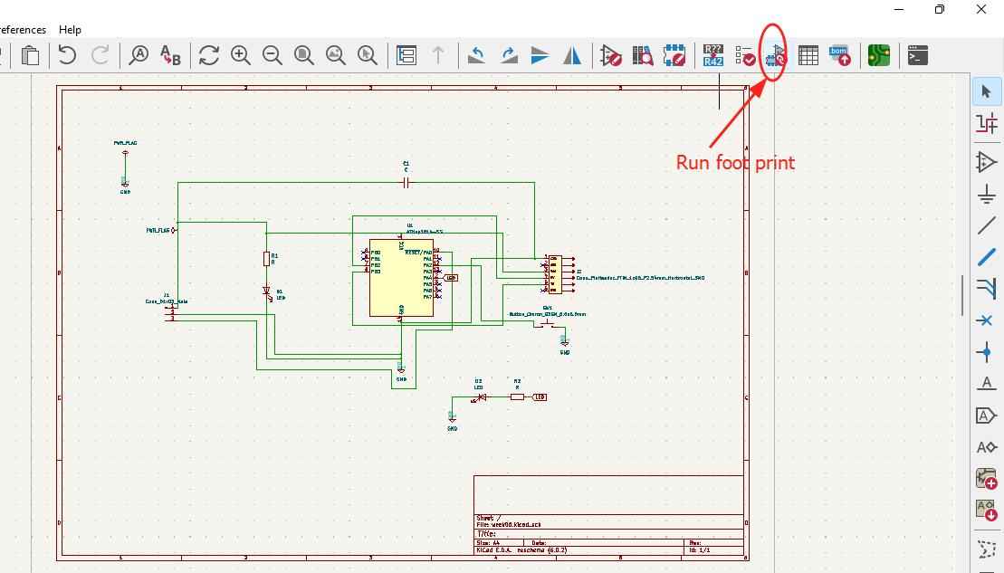
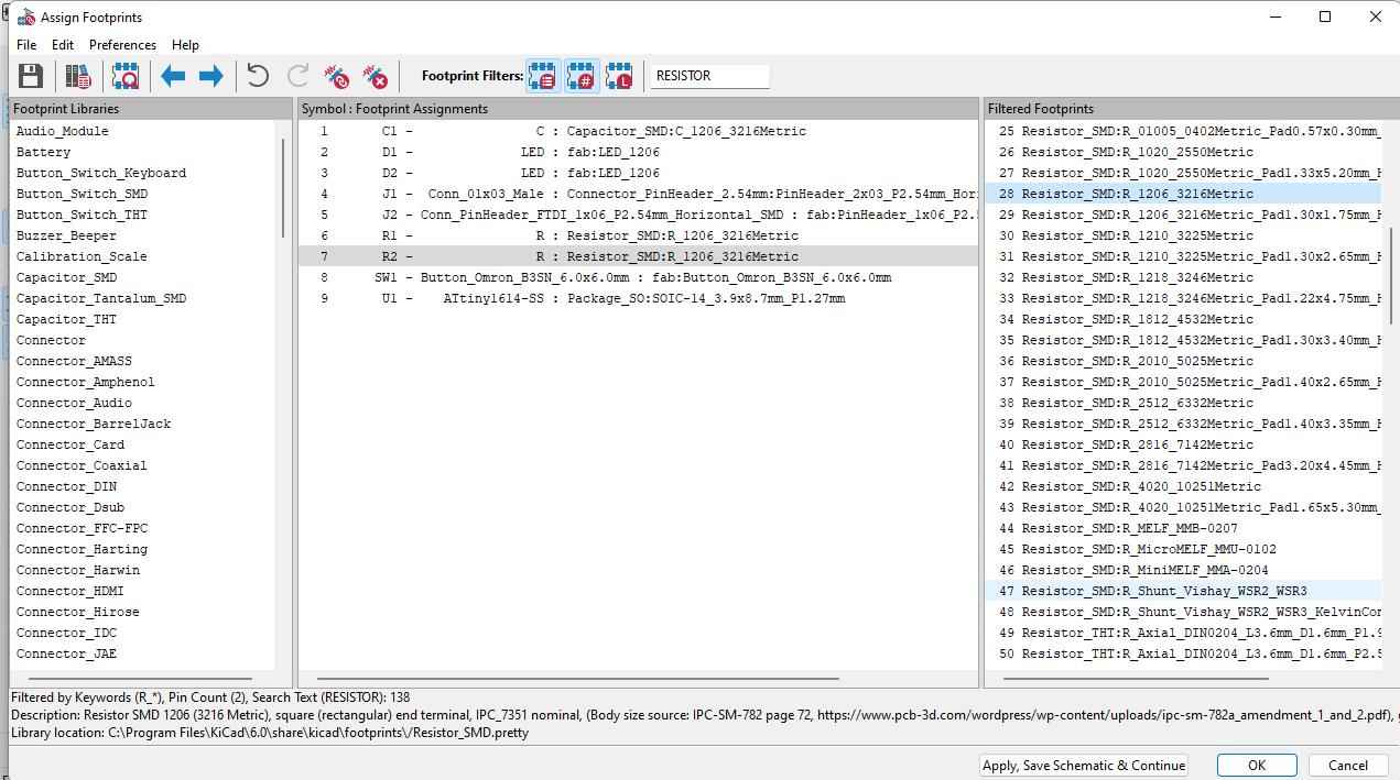
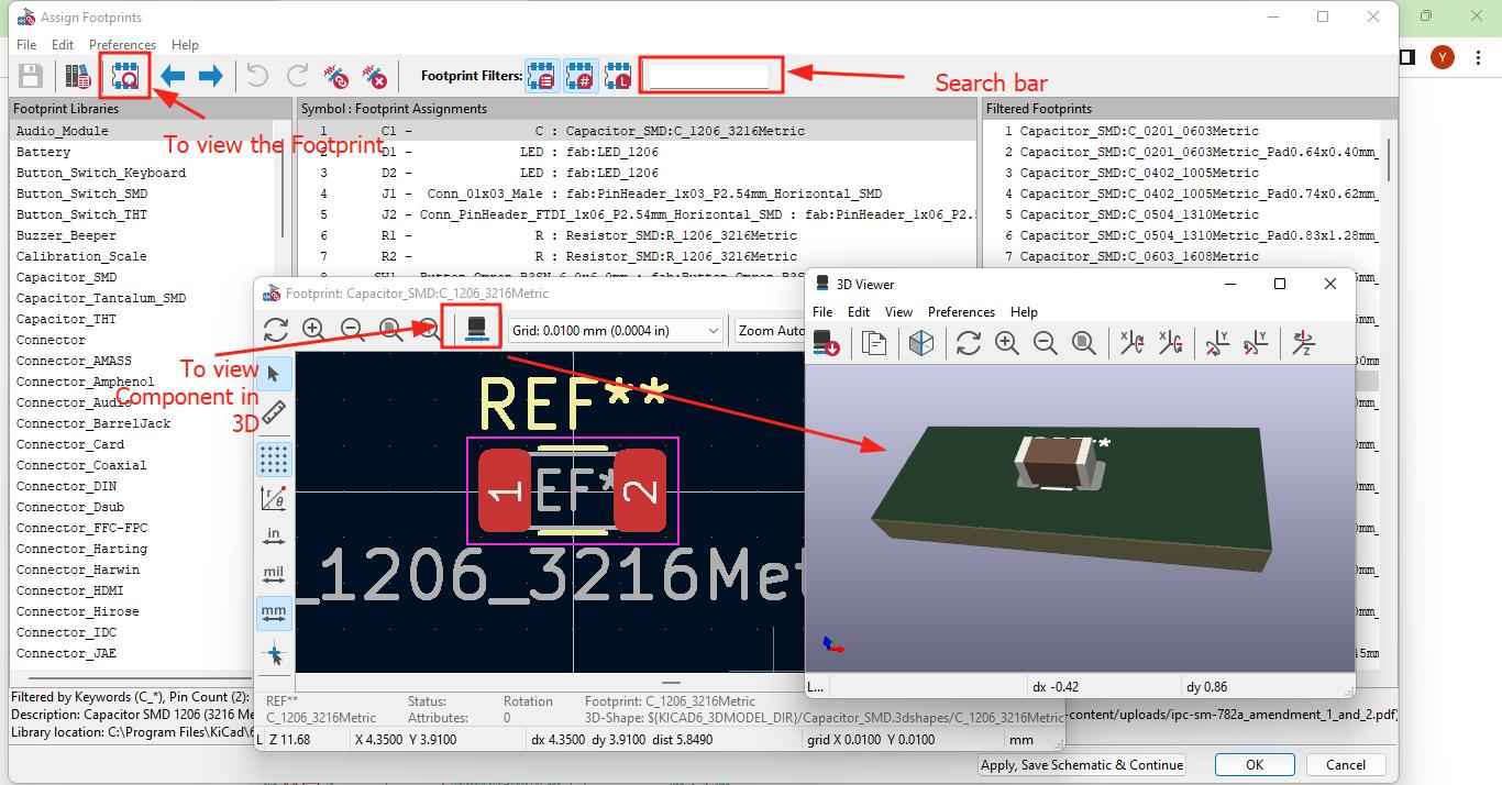
- I assigned the footprints for each components. Click on tool >> Assign Footprint or click on the symbol shown below in image >> Run Footprint Assignment tool. Select footprint for each components using search bar.
- We can view the footprint in 2D and 3D as well.
Updating Board editor
-
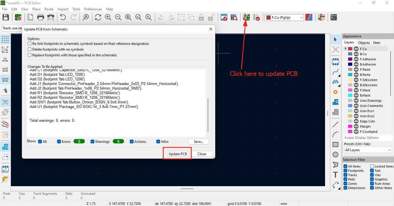
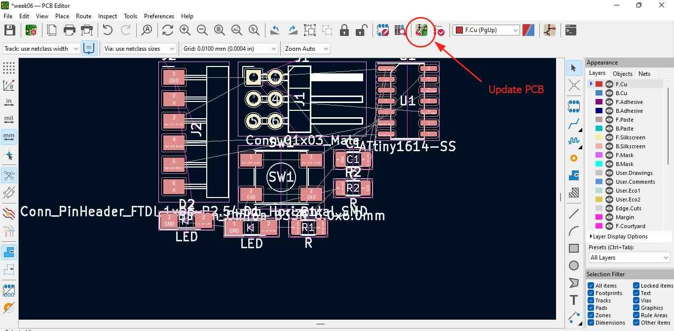
I updated the PCB and imported the PCB design on work space.
-
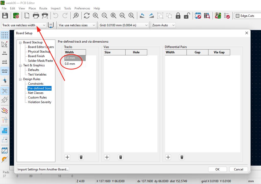
I arranged the component and routed. Make sure that the rout width is 0.4mm and the track width is 0.8mm.
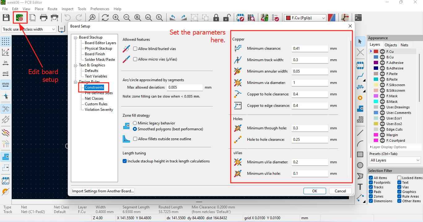
- Click on Edit board setup > design rules>constraints. Set the parameter.
- Then I defined the size under design rules and set the parameter for the route and edge cut 0.4mm and 0.8mm.
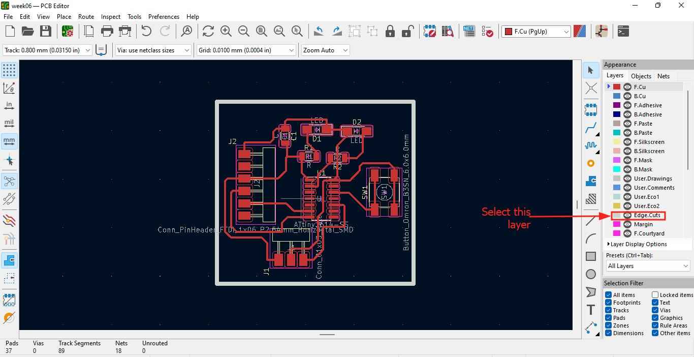
- Click on draw line option or the rectangle tool at the right side to draw the edge cut. Select the edge cut layer. I kept the edge cut width of 0.8mm.
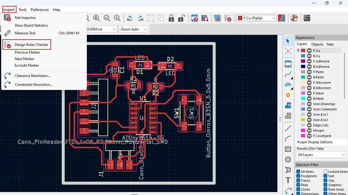
- To inspect the errors go to Inspect > Design rule checkers >> Run DRC. I have some warnings and no errors and I think it is going to work. My instructor Zina told me that warnings are acceptable and wont hamper much. So I continued on exporting the file.
Saving and exporting files
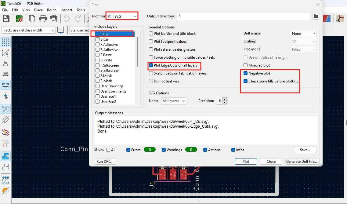
- Go to File menu >> Plot >> Format SVG>>
- In include layer choose/check F.cu(front copper layer).
- In general option:
- Choose check ->> zone fills before plotting
- Choose Negative plot.(If done negative ploting for F.Cu do same for Edge.cuts as well because the sizes gets differed by the black background)
- I think it is optional to check Plot edgecut on all layers while plotting F.CU.
- Then click on plot to export. If we do not choose the directory folder it gets saved in the project folder(current) by default.
- To export Edgecut select Edge.Cuts.
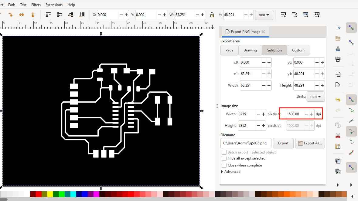
- I checked Plot edgecut on all layers while plotting F.CU under general options and then clicked Plot. I did not do negative plotting for edge cut because Edge can be in black colour. The SRM cuts of black lines. If I do negative plot I have to do Invert in MODS.
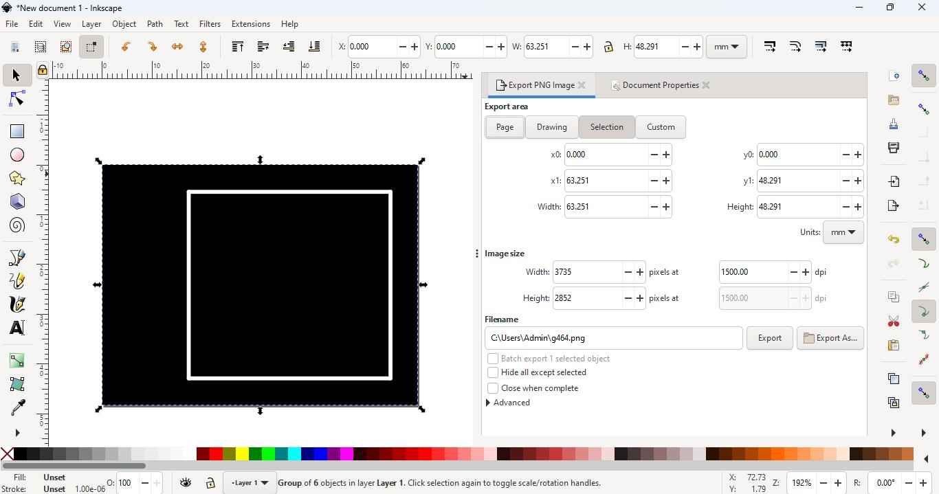
In order to print the board we use mods and mods reads PNG file. To convert the SVG to PNG we use INKSCAPE. - Open the SVG file with INKSCAPE - Select the image and click file ->> Document properties and do resize the page to the content. - Select the file and go to File ->> Export PNG Image. Make cure that the dpi should be minimum of 900. - Rename the file and choose the directory and click on Export.
Design file for this week is here