Wild Card Week 
Assignment
Design and produce something with a digital fabrication process (incorporating computer-aided design and manufacturing) not covered in another assignment, documenting the requirements that your assignment meets, and including everything necessary to reproduce it.
See more info and recording of the lecture here.
Vacuum forming
Design
The annual Icelandic Fab Lab Bootcamp was held in Fab Lab Neskaupstaður in 2023. Móses, the Fab Lab manager, showed me how to do vacuum forming with the Mayku FormBox.
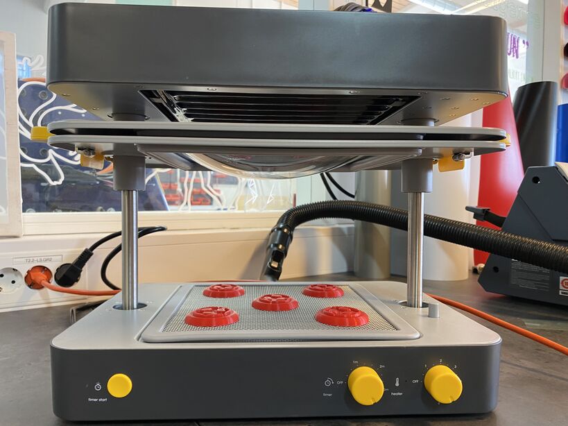
The Mayku Formbox is a basic 200x200mm vacuum forming machine. Its heating element goes up to 340°C You need to connect a vacuum cleaner to it for it to work. It works fine, but I think I would find it annoying to have to bring the vacuum cleaner every time I used the vacuum former.
 My first attempt.
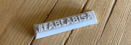
First I brought a rectangular 3D print with #FABLABISA inscribed on it. Móses said that the object was rather small, the edges needed to be rounded and he also showed me examples of details similar to my text not coming through in the plastic sheet.
 Vacuum forming examples. Sharp corners and small details don't work well. The text JÓL (Christmas) in the upper right corner doesn't come through at all.
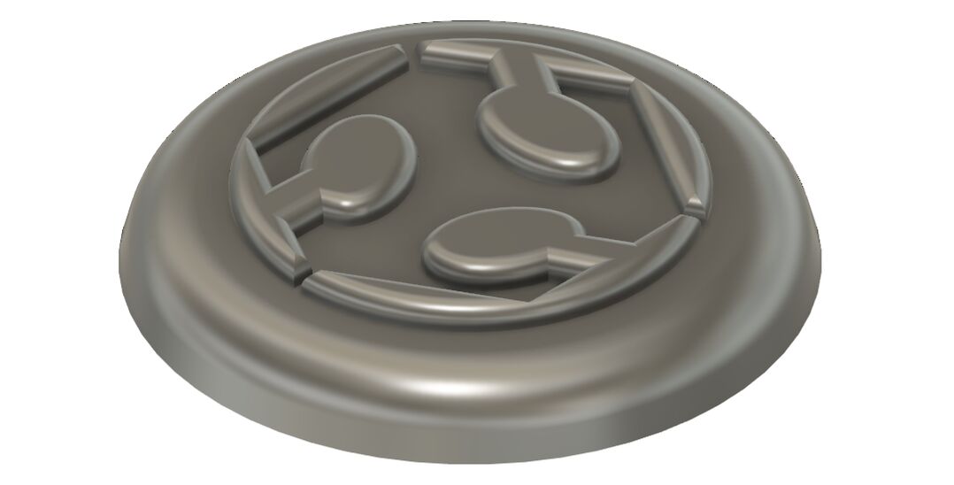
He also mentioned that circular things tend to work the best. That makes sense, the stretching will be uniform and there are no corners where creases can form in the plastic sheet. I decided to go with the Fab Lab logo instead. I rounded the chocolate button shape and the logo as much as the geometry would allow, and showed Móses a finished print.
I used a Mayku Clear Sheet, which is made of PETG and is food safe. The official Mayku sheets are not cheap.
 Now that's a better candidate for vacuum forming.
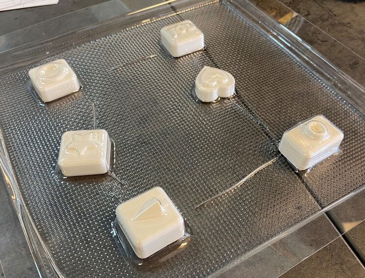
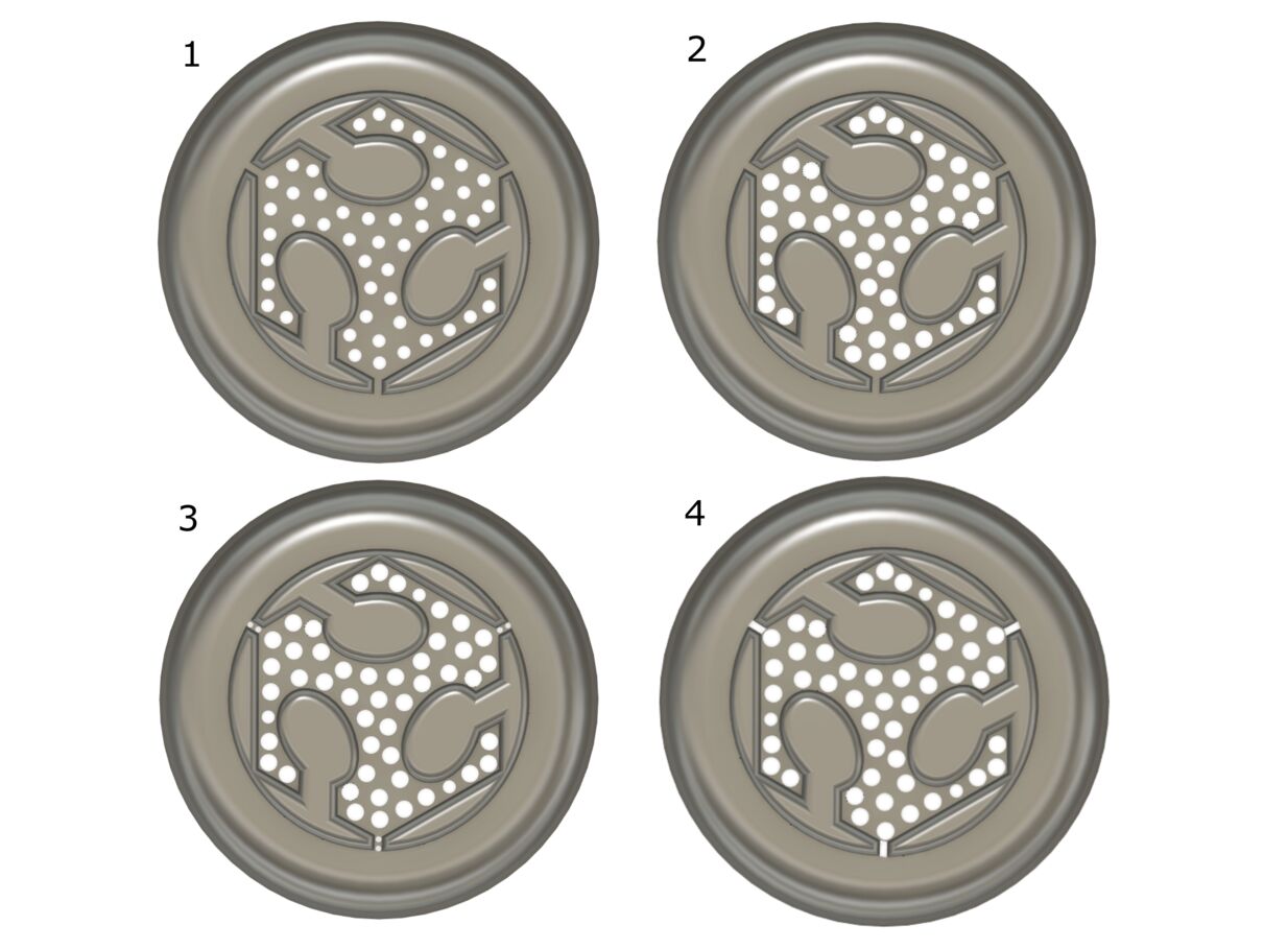
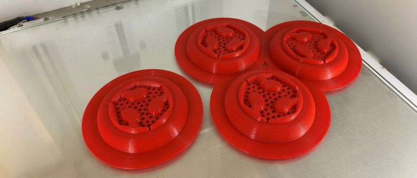
This should work nicely, said Móses, but there is a question whether the pocket in the middle will be rendered in the plastic sheet. I decided to try making holes in the middle to let the air out. printed four versions of buttons with holes in the middle, for a total of five buttons:
- No holes
- 1.5 mm holes
- 2 mm holes
- 2 mm holes with small holes in the three smallest crevices
- 2 mm holes with rectangular holes in the three smallest crevices.
 Buttons with holes added to draw vacuum through the center of the part.
Design files
Here's the Fusion model of the Fab Lab chocolate button:
Download failed #FABLABISA chocolate Fusion 360 model
Download chocolate button Fusion 360 model
3D printing
 Completed 3D prints.
Vacuum forming
When the prints were complete, we connected a vacuum cleaner to the FormBox and heated it up. Móses told me that the sheet needed to be heated up until it droops 2 or 3 cm down. Then it's soft enough to form.
 Sheet is hot and drooping and ready to form.
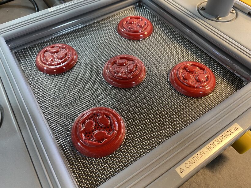
Then the handle locks are released and the frame with the sheet is quickly lowered onto the bed containing the 3D printed positive forms. The vacuum is held for a minute or two and the sheet is allowed to cool down a bit. Then it's ready!
 Done!
Done!
To my surprise, all the forms came out well. Apparently the tiny crevices in the logo were enough to get the air out of the middle part. The button with no holes actually came out the best!
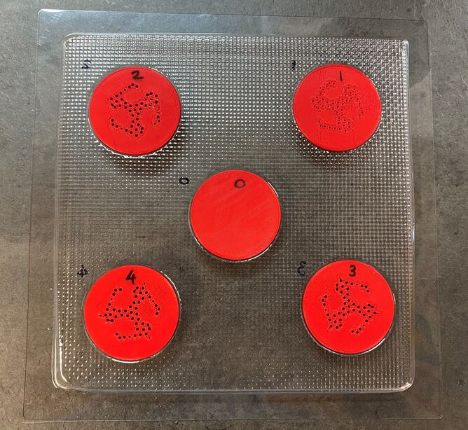 Better label both the buttons and the sheet to remember which is which.
I tried measuring the depth of the pocket in the middle of each button with a caliper and they seemed to be the same, whether there were holes in the forms or not.
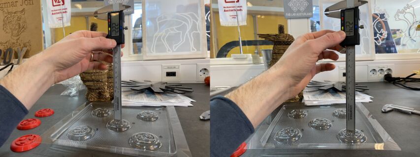 Measuring the depth in the middle.
I like vacuum forming but its applications are limited. It would be nice to host a short class on chocolate mold making here at the Fab Lab, but I don't know what else I would use the vacuum former for. Mostly it's used to make packaging, and I don't make any packaging.
Chocolate casting
I followed instructions from the Icelandic newspaper Morgunblaðið, so they may not be useful to you.
First melt the chocolate slowly in a water bath. Don't let any water get into the chocolate! You heat it up to 50°C.
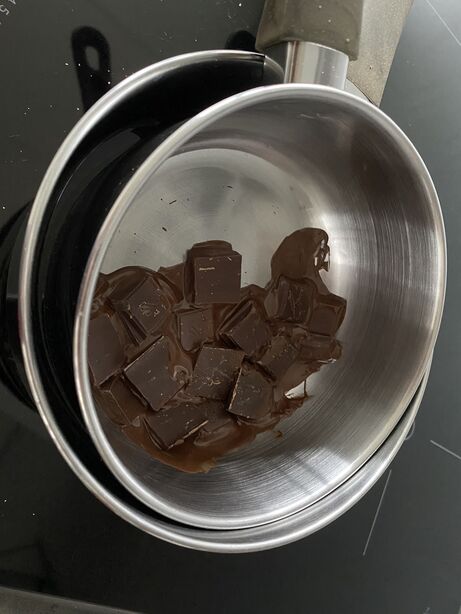 Melting the chocolate.
Then you let the temperature drop to 42°C and you add a third of the same kind of chocolate (chopped) to the pot. Stir it into the melt.
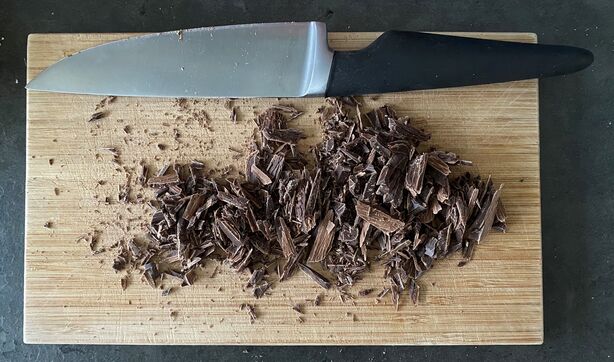 Chopping the rest of the chocolate.
 Putting the chopped chocolate into the pot.
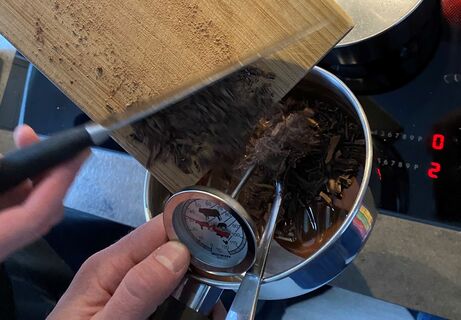
Then you let the temperature drop down to 32°C. Now the chocolate is tempered and you can pour it into the molds.
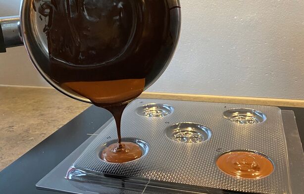 Pouring into the molds.
I also shook the molds to flatten out the bottoms of the buttons.
And here they are, lined up with the 3D prints that created them.
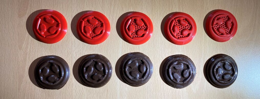 Row of chocolate Fab Lab buttons. They all came out well. I would skip the holes in the middle next time.
Now it's time for testing. Is the chocolate tempered or not?
I suspect that my next attempt may be more successful, since I won't have to take pictures and videos while I try to get the temperature profile right.
Further experimentation
It would be interesting to try printing the original Fab Lab button model with an increased distance between the 3D printed lines. I think that would make it possible to draw vacuum through the part without having to draw holes manually. And the top surface texture might be nicer, too.
Update
The meat thermometer that I used isn't very precise. I then found this tutorial, which describes a method to temper chocolate without a thermometer, using a microwave. This was quick and easy, and the Fab Lab chocolate buttons snap apart!
Success!
FPGA (Field-Programmable Gate Array)
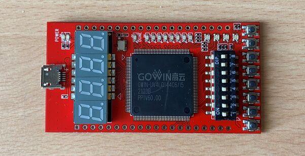 The Runber FPGA board. I think the program is supposed to blink the eight LEDs above the FPGA chip, but the tutorial isn't entirely clear about it.
Why
I've been curious about FPGAs for some time, for four reasons:
- I took the course Computer-Controlled Hardware in engineering school at the University of Iceland. One of the lecturers is an FPGA designer at the prosthetic company Össur. He showed how the company's Power Knee has developed over the years from a large, complicated circuit board with lots of components to a much smaller footprint, essentially containing only a microcontroller and an FPGA. The FPGA can contain any digital circuitry, which is really interesting.
- My wife gave me the book Einstein's Shadow for Christmas a few years ago. It's an entertainingly written account of the quest to photograph a black hole. It involved extremely high-speed FPGA chips which made the Event Horizon Telescope possible.
- The astonishing optical encoder in the Dexter robot arm. You need to see this example of micro movement with Dexter.
- In the 2023 Fab Academy Student Bootcamp, Krisjanis Rijnieks mentioned that ordinary people now have the opportunity to design digital chips and have them made, using open source toolchains like Google Silicon. Google also offers the Open MPW program which is a lottery where you can submit your chip design and if you're lucky, Google will pay for the chip fabrication. I also discovered the Zero to ASIC course from Matt Venn, where he teaches people to design Application Specific Integrated Circuits from scratch and has them manufactured for them. Exciting stuff! Chips are designed using VDHL or Verilog, which are hardware description languages. You also use these languages to program FPGAs. Before committing a chip design to manufacturing, people usually test it on an FPGA.
In Wild Card Week, I thought to myself: If I don't try an FPGA now, I probably never will. For this week, I ordered the cheapest FPGA board that I could find ($30) that still has a set of tutorials available, the Gowin RUNBER board from Seeed Studio.
How
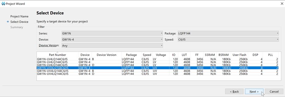
An FPGA is a circuit that you design with a hardware description language. The unit of computation is is one bit, which can be a 1 or a 0. The FPGA consists of lots of Look-Up Tables (LUTs), which specify what happens when ones or zeros enter them. These LUTs form logic gates which can be combined to make any circuit, even a whole ARM microcontroller! Indeed, many FPGAs are programmed to contain a microcontroller core as well as additional digital ciruits. The Gowin GW1N-4 on my board has 4608 LUTs with four inputs each.
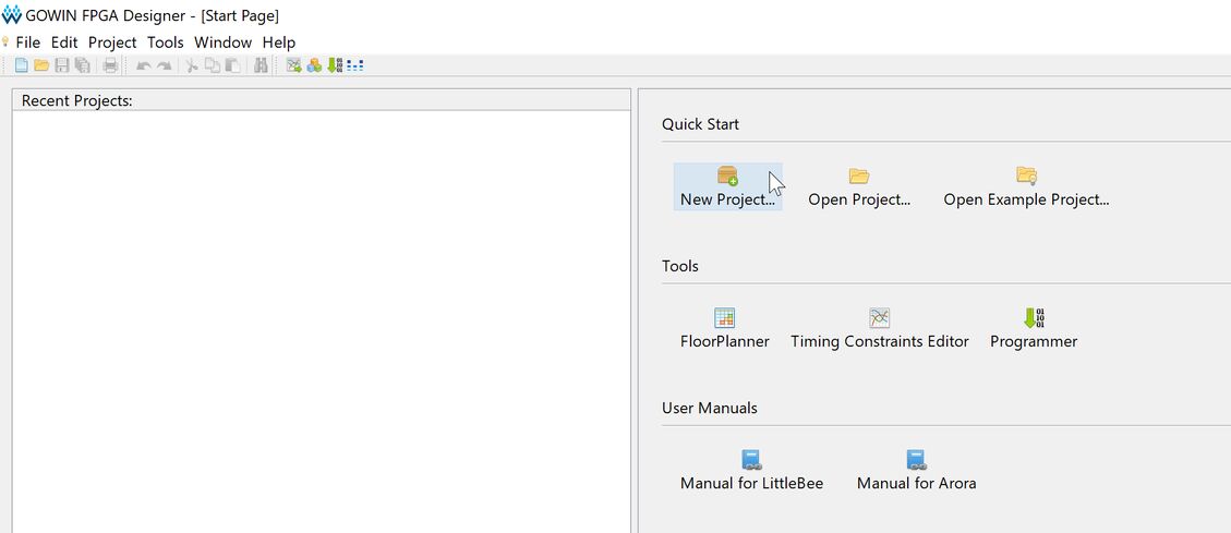
I managed to get a license by sending an email to Gowin customer service and then I followed the first tutorial in this PDF. The circuit blinks eight LEDs, one at a time. In Gowin FPGA Designer, I created a new project:
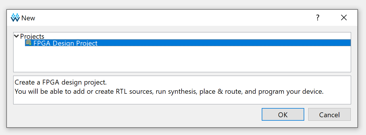
I selected FPGA Design Project:
And then I selected my FPGA chip:
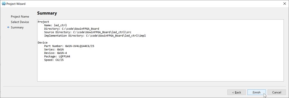
I got a summary of the project settings before finishing the setup:
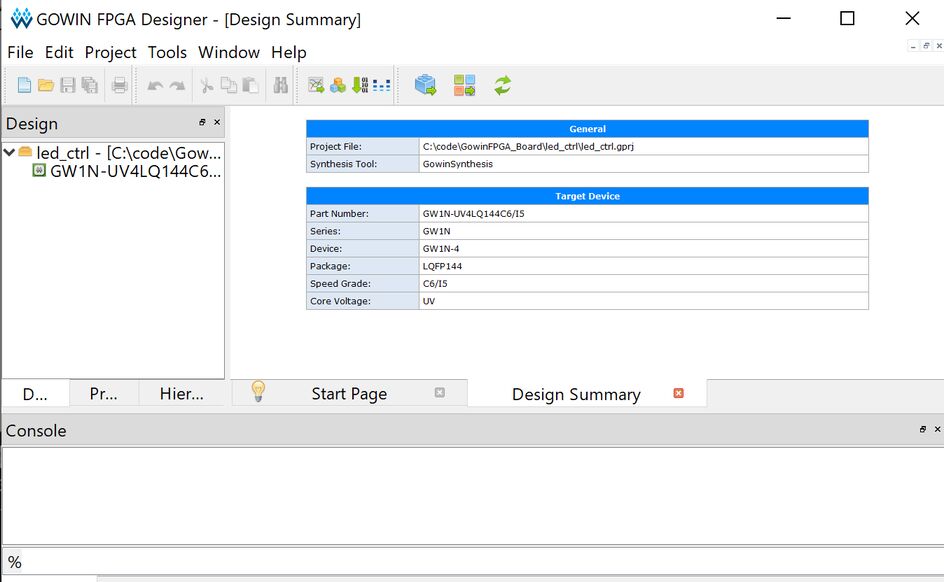
Now I had a new FPGA design project. So far so good:
I created a new Verilog file and pasted the code from the tutorial. Then I clicked Synthesize:
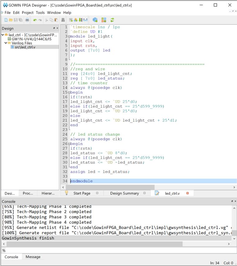
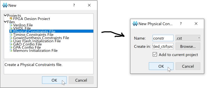
That seemed to work OK. Then I went into Tools -> Floor Planner to see how the circuit looked inside the FPGA. I got an error. Then I looked a little further in the tutorial and found that I needed to create a constraints file, where I specify which pins I'm using and what they are. I went into File -> New, selected Physical Constraints File and gave it the name constr.cst:
I just copied the code from the tutorial and pasted it into the constraints file. This is how it looks in the editor:
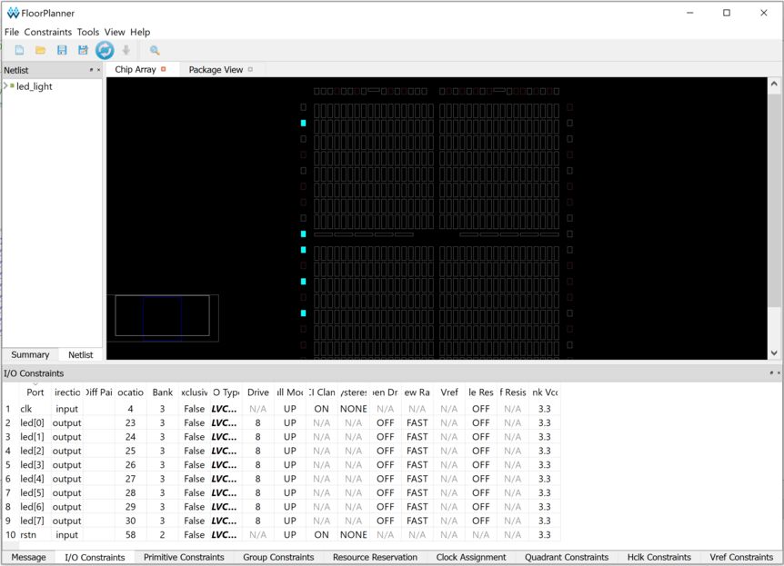
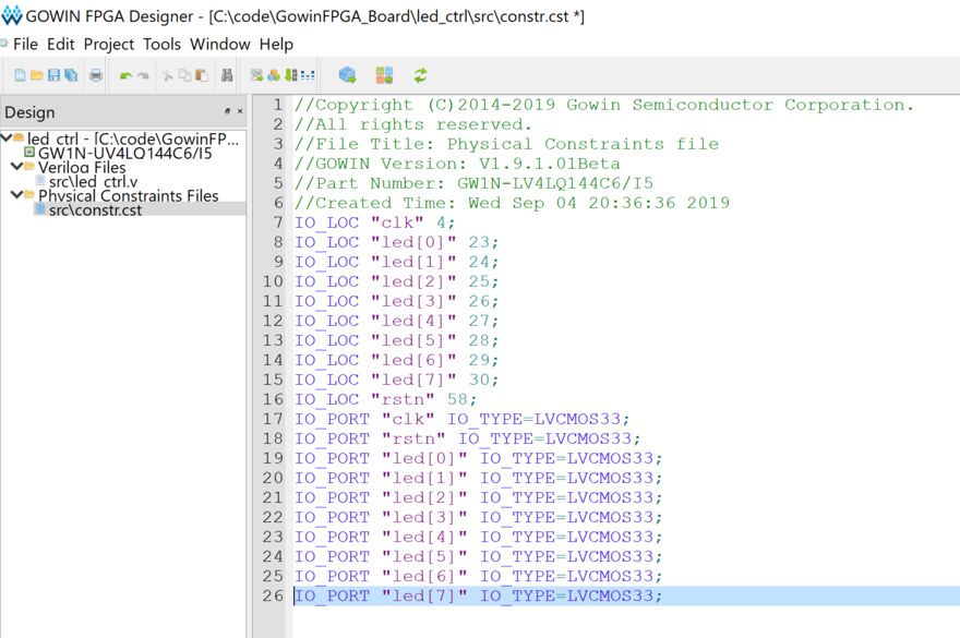 The constraints file defines eight output pins that are supposed to turn eight LEDs on, one at a time.
Now I could go into Tools -> Floor Planner. I got a graphical representation of the chip. I would expect eight pins to be highlighted in blue, but only six pins are highlighted. But I wouldn't know how to fix the code, and the messages in the terminal seemed positive:
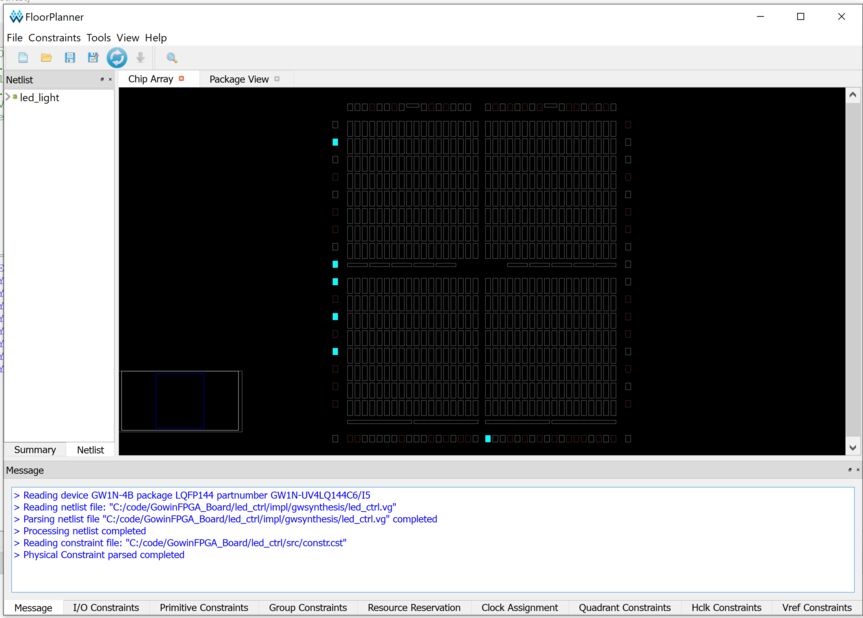
So I soldiered on. I selected the I/O Constraints at the bottom of the window and got a list of the constraints that were defined in the .cst file:
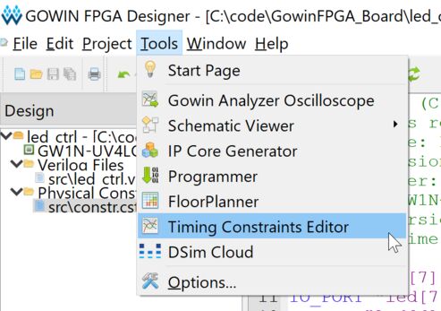
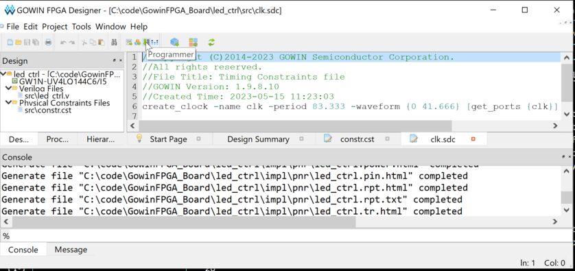
The third and final file I needed to create before programming the FPGA was a timing constraints file. In FPGAs, everything is counted in clock cycles, and you need to define the clock frequency. I opened the Timing Constraints Editor:
There I created a Timing Constraints file with a period of 83.333 nanoseconds and a frequency of 12 MHz:
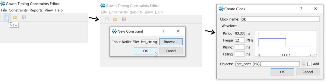
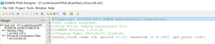
The timing constraints file only contains a single line of code specifying the clock speed:
Then I selected Run Place and Route. That's the button with four colored squares that looks a bit like the Windows icon. I got a bunch of Generate file completed messages in the terminal, which seemed promising:
If you look again at the image above, you can see the mouse hovering over the Programmer icon, which is a green downward arrow. I now pressed it and hoped for the best. I have no idea what I am doing.
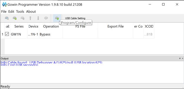
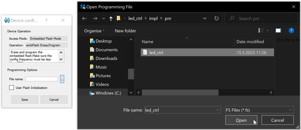
The programmer found a USB device, so I clicked Program/Configure. Here the tutorial ends, but I still needed to make some selections. I found the manual for the Programmer in the Gowin software directory and followed instructions that told me to select Embedded flash mode and select the .fs programming file in the dialog:
When I clicked Save I got an error:
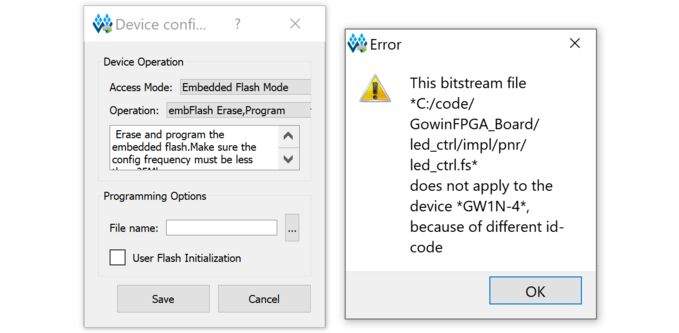
This seems like a simple error, all I have to do is select the right chip. I tried selecting all the chips that have similar names to mine (GWIN-4, GWIN4B, GWIN-4D and all their versions). I had to select the chip both in the Floor Planner and in the Programmer. But nothing worked. I don't know where to go from here, so I'll stop.