Week 6. Electronics Design
Group Assignment
Takeaways:
* Before any testing is done, the Oscilloscope needs to be calibrated. to conduct this calibration: connect the probes from your device to the 2V terminal. We used alligator clips to do this. Then hit Autoset.
Individual Assignment
KiCAD
As a beginner in Electronics, I decided to stick with KiCAD as my software of choice for this week.
I wanted to make a board that had the attiny1614 as the micro controller, with the following components:
1. LED
-
Resistor
-
Capacitor
-
Button
-
3 point connector for a
servo motor -
FTDI connection
-
UPDI connection
I wanted to add the servo motor since my project revolves around drones and I wanted to control the control bodies with servos.
Adrians’ Adrianino was a great source of inspiration as he used the attiny1614 as well.
Work flow:
- Install KiCAD
-
Add Fab Library. >I followed the given instructions:
- Clone or download this repository. You may rename the directory to fab.
- Store it in a safe place such as ~/kicad/libraries or C:/kicad/libraries.
- Run KiCad or open a KiCad .pro file.
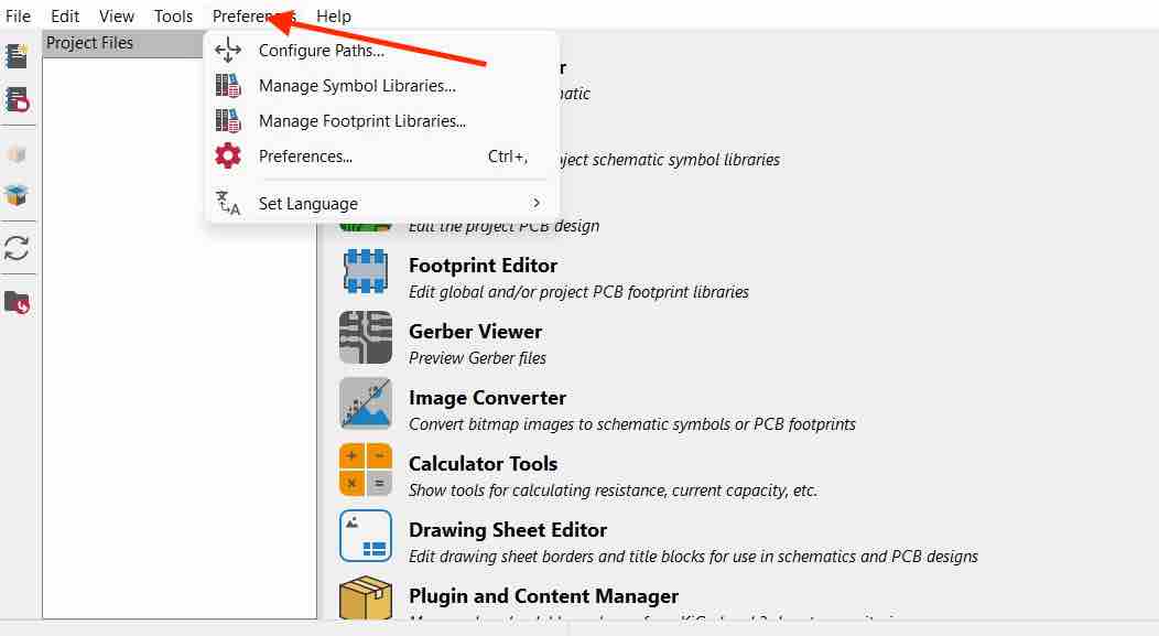
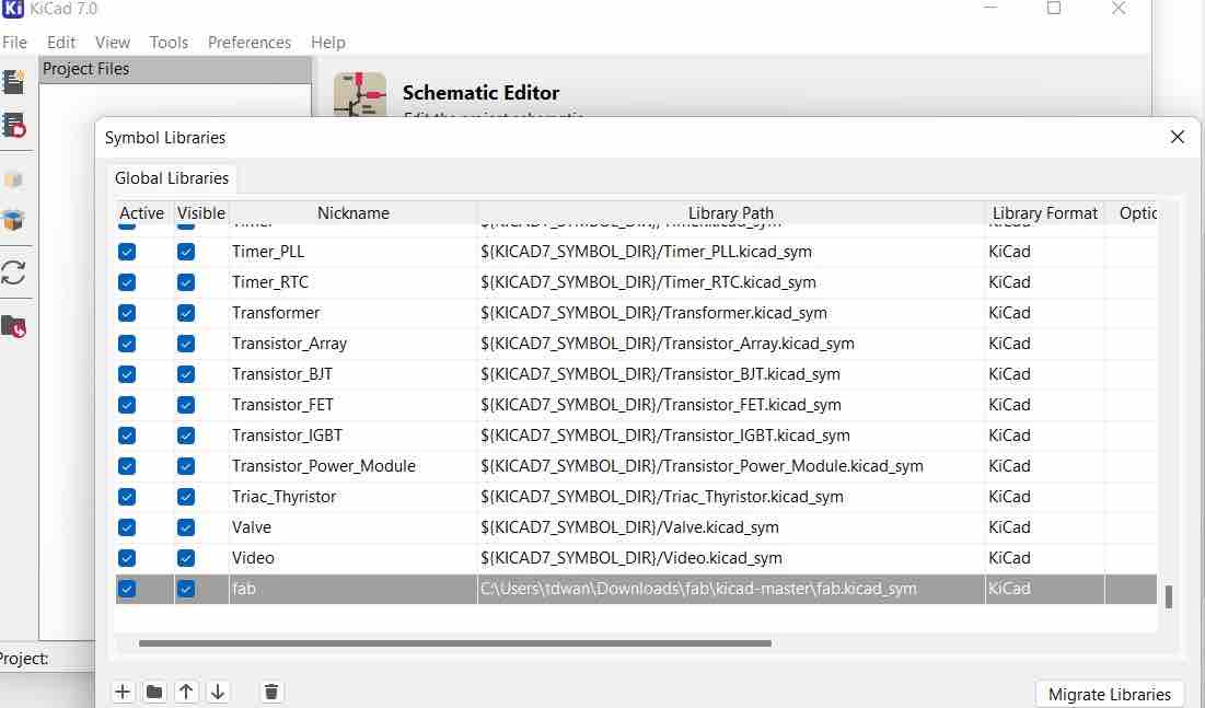
- Go to “Preferences / Manage Symbol Libraries” and add fab.kicad_sym as symbol library.
- Go to “Preferences / Manage Footprint Libraries” and add fab.pretty as footprint library. Go to “Preferences / Configure Paths” and add variable named FAB that points to the installation directory of the fab library, such as ~/kicad/libraries/fab or C:/kicad/libraries/fab. This will enable the custom 3D shapes to be found. The 3D shapes project has just started and most of them have to be populated still.
- In KiCAD, open
New project
Short cuts:
m = move component
r = rotate component
a = add component
ctrl+c, ctrl v = copy/paste
g = grab component and connection
e = assign value (after hovering over component)
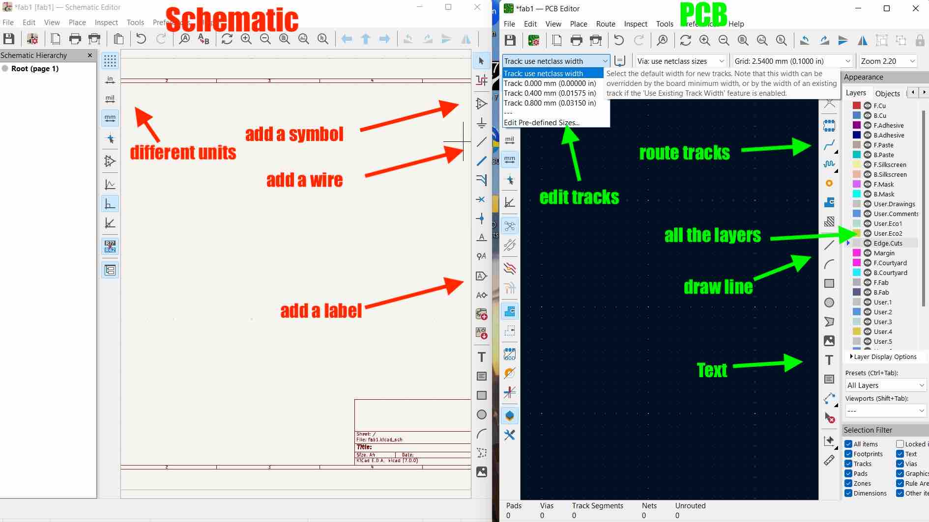
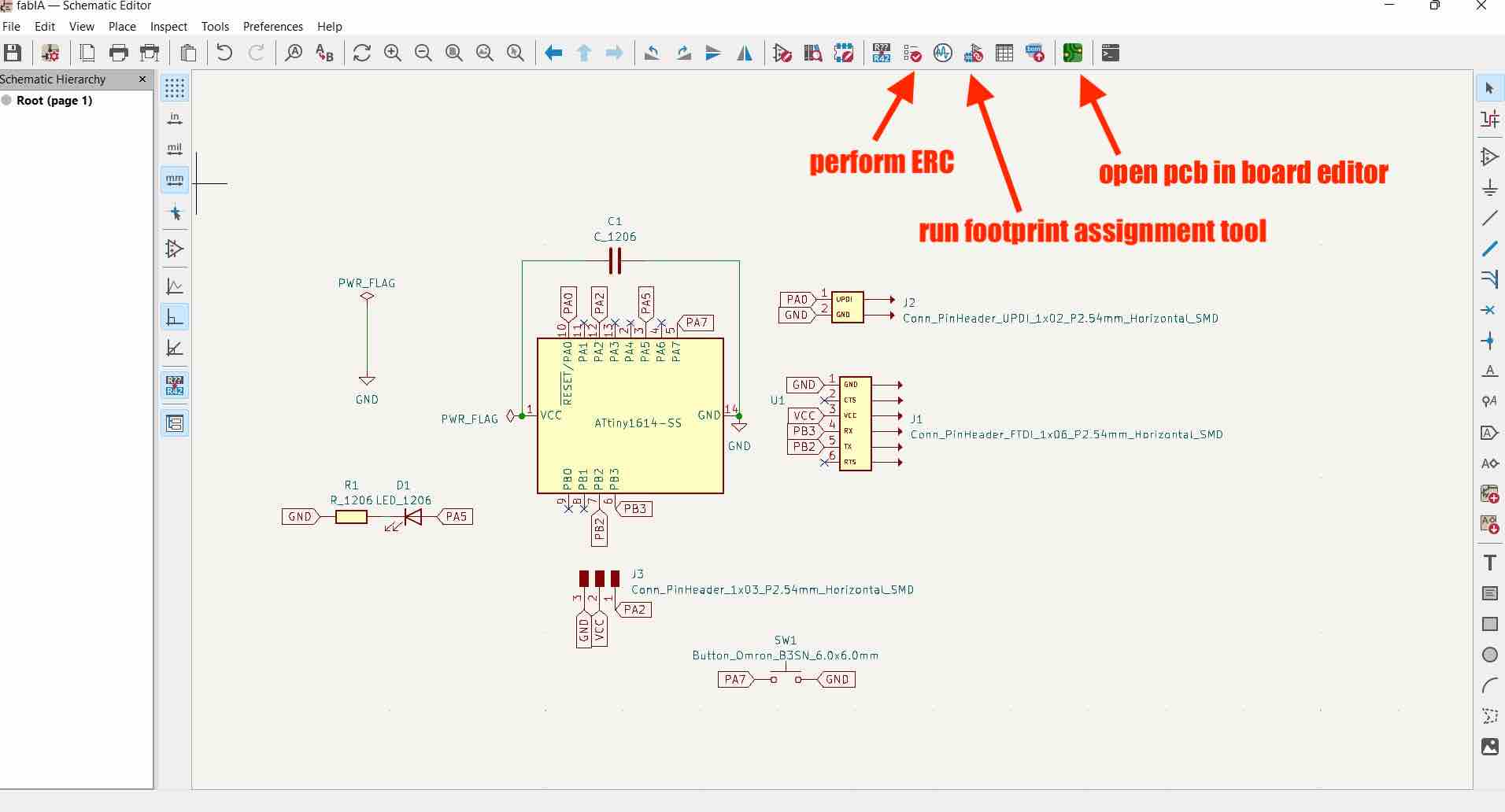
Schematic:
- Choose the
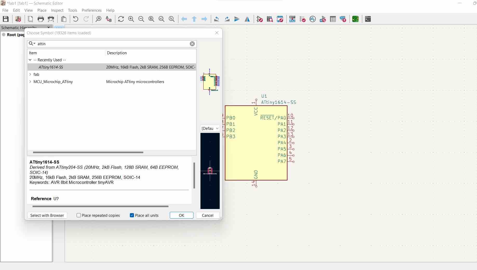
.schfile - Click
aand addattiny1614SS(pop up window allows you to choose) - add a capacitor, resistor, LED, FTDI, UPDI, 3 pin male connector (all from the fab library)
- Quick Guide:
- You can add
wiresto connect the components or make use oflabels - refer to the attiny1614 datasheet to see what components needs to be connected to which pin.
- create labels for PA0, PA2, PA5, PA7, PB2, PB3, VCC and GND
-
Connect all the labels to the necessary pins. >PA0 - UPDI
PA2 - Connector
PA5 - LED
PA7 - Button
PB2 - FTDI TX
PB3 - FTDI RX
-
do the same with GND and VCC
- add
no connection flagto unused pins - add
PWRand 2GNDflags. - Connect one GND to PWR flag
- add the other GND to the GND of the mcu
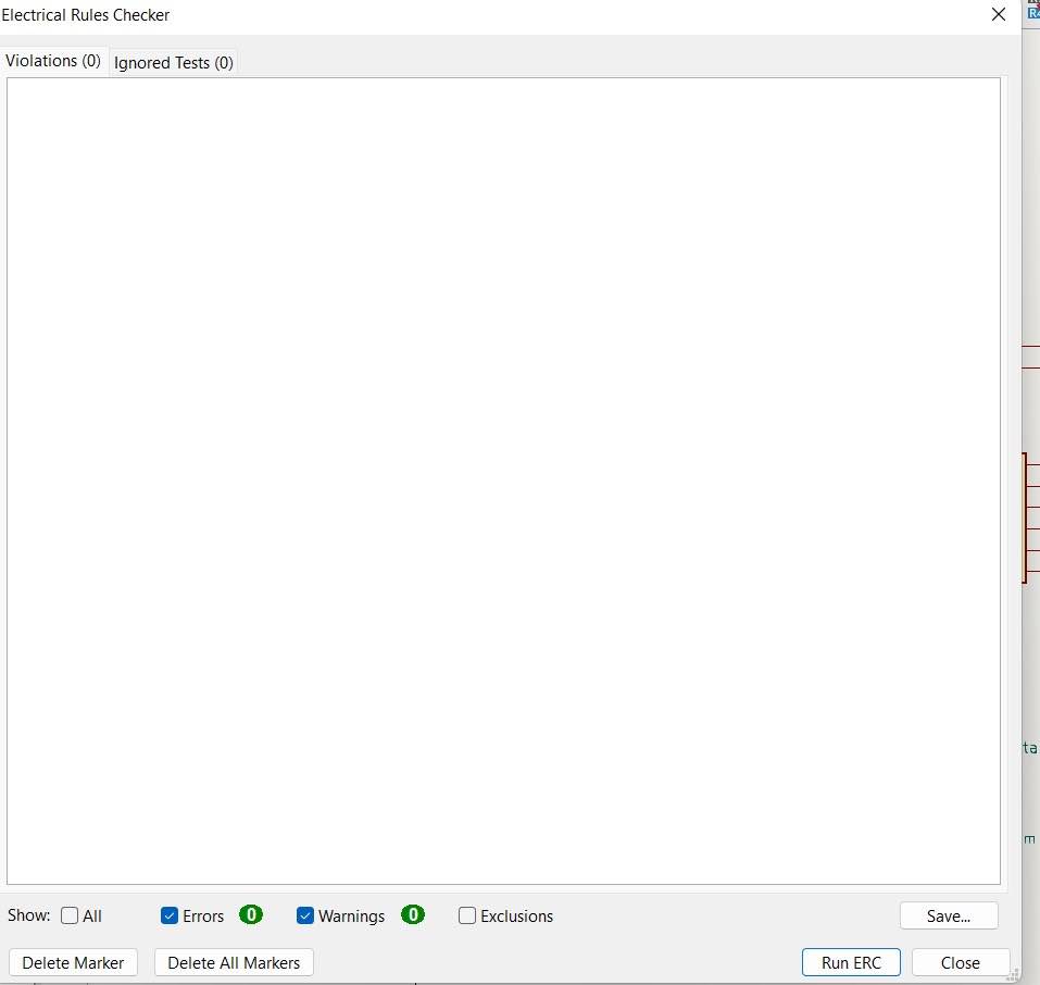
- run the
ERCfrom the top right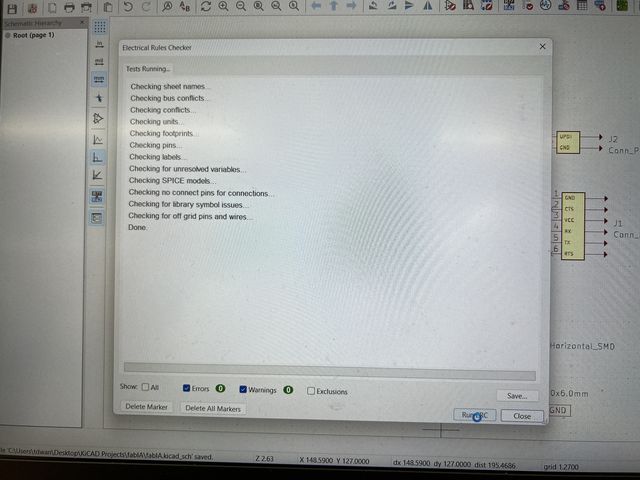
- assign
foot printsby hitting theRun footprint assignment tool - select which component you want to assign a footprint too, and search for it and apply ones from fab
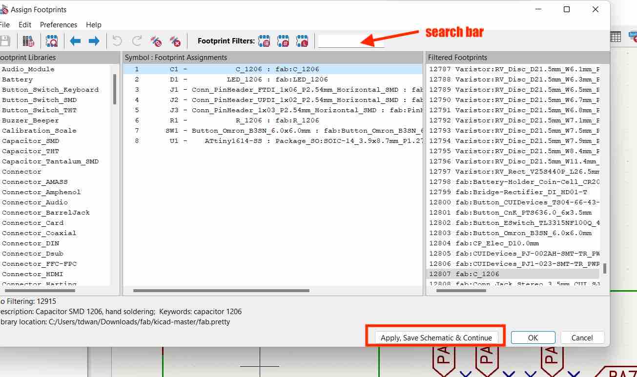
- Once done,
Apply, Save Schematic & Continue - Final schematic:
Shortcuts:
X: route tracks
u: to select the entire track
d: to drag the components and it’s tracks
m: move just the component
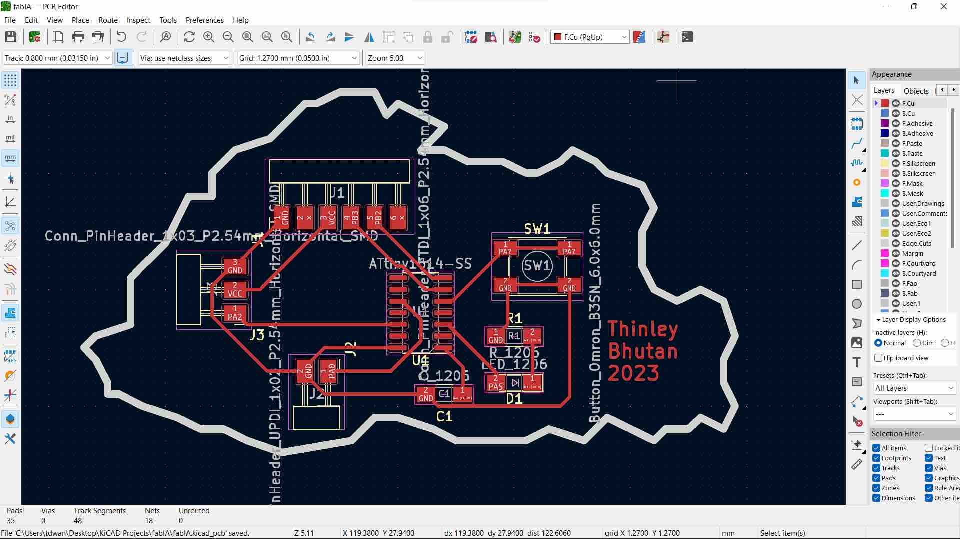
PCB:
- Open the
PCB editor - Hit
Update PCB with changes made to schematicorF8to add all the components from the schematic to the PCB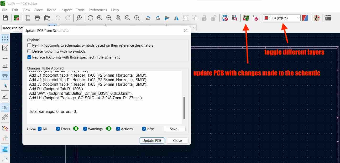
- move and adjust components keeping in mind where they are
- edit the track width by
editingthe Track on the top left - add
0.4mmand0.8mmand hit ok Route Tracksor hitXin the FCu layer. Connect all the necessary components- go to
editsand useEdit Track & Via propertiesto apply the track widths to all. - select the
edgecutslayer and draw the outline of the board using the line tool. - I wanted to make my outline the map of Bhutan, so I went to
file->import->graphics-> in drop down, selected my custom svg and selectededgecutsin thegraphic layer.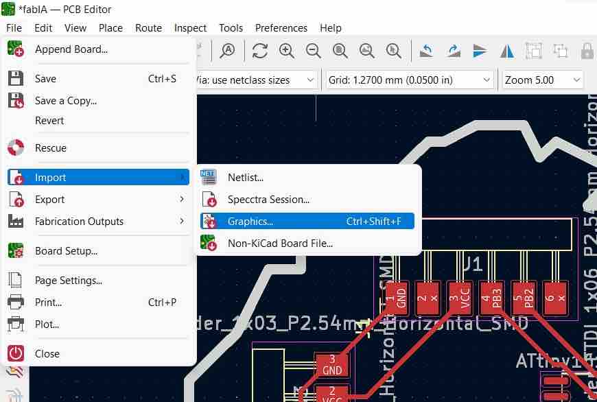
- Ensure to use 0.8mm track width
- open the
Design rules checker windowand run theDRC - I ran the DRC, and ran into an error:
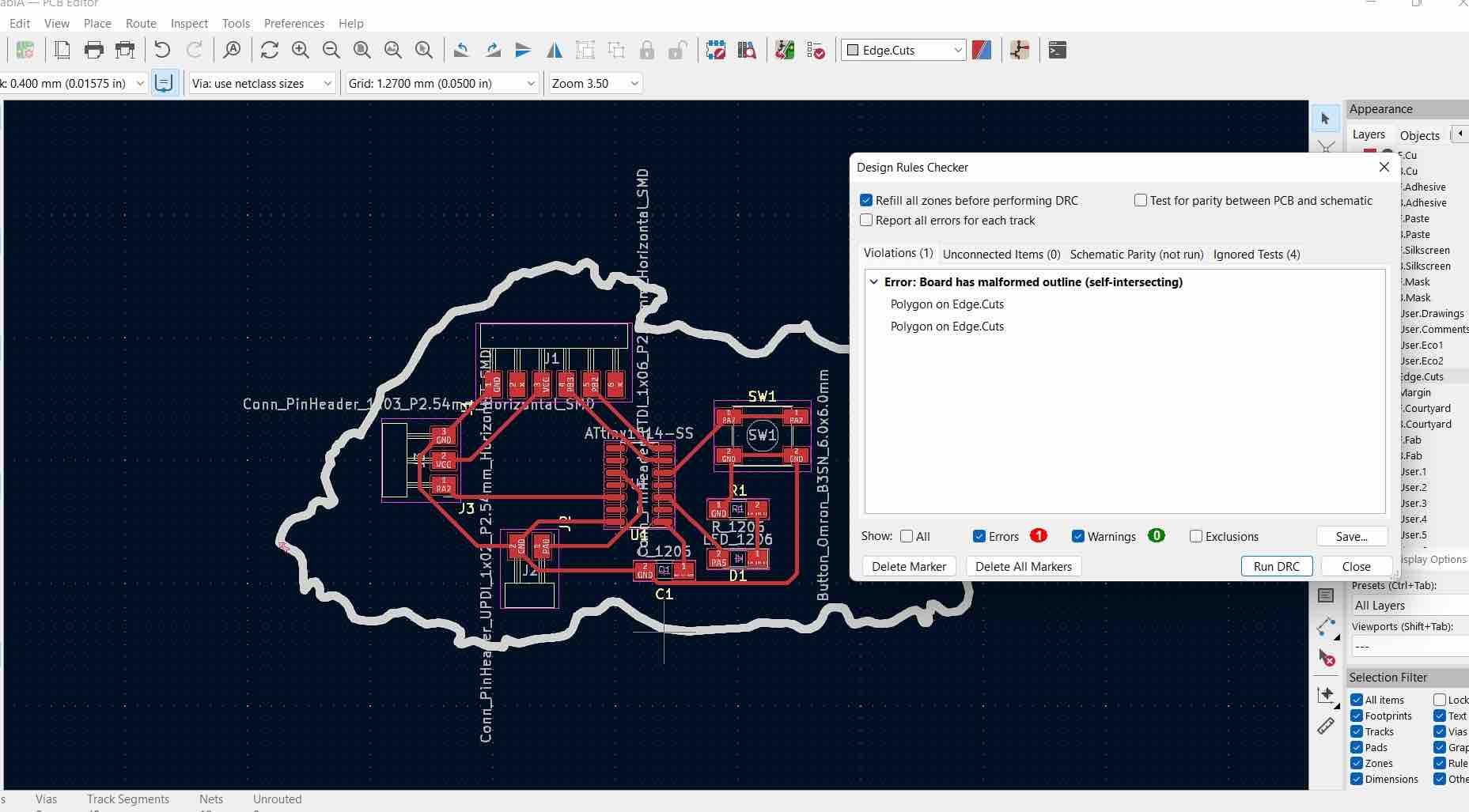 No matter what I did, I couldn’t fix it. I tried editing the fill, stroke width but nothing worked.
 - I then decided to trace over the map with the
linetool and made a rough outline of Bhutan and it Worked!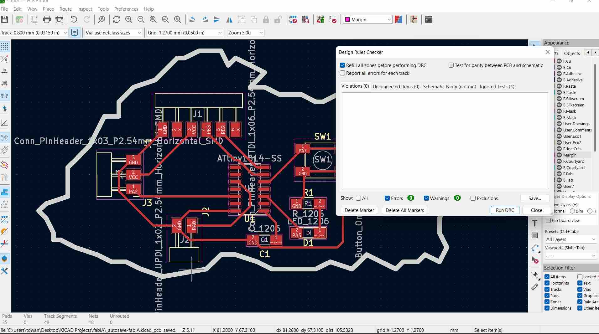
- In the F.Cu layer, I added the
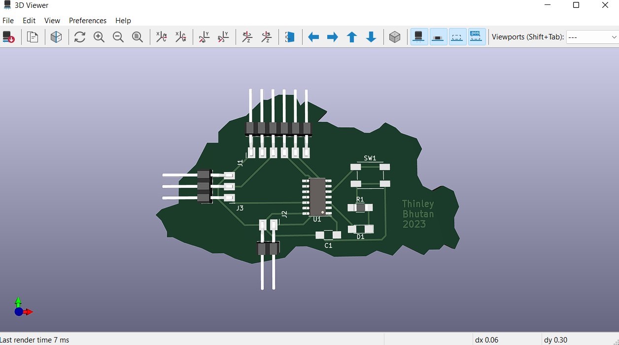
text. - My Final board:
- Then I went to
file->plotand the plot drop down opened up: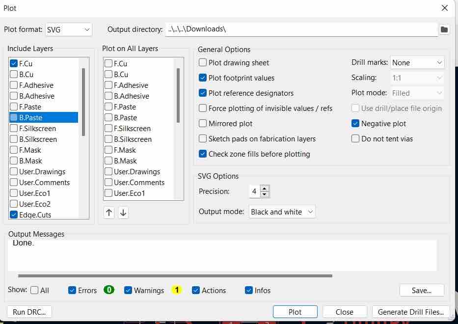
- I selected the format to be
svg, andnegative plot.I converted the SVGs ininkscapeto png/jpg. -
To plot the
exterior+interior, I did the same but selectedF.CuandEdgeCutsonplot all layers
-
to plot the interior traces and exterior traces separately, I selected both the
F.CuandedgeCutsin theinclude layersoption and unselected them from theplot all layers

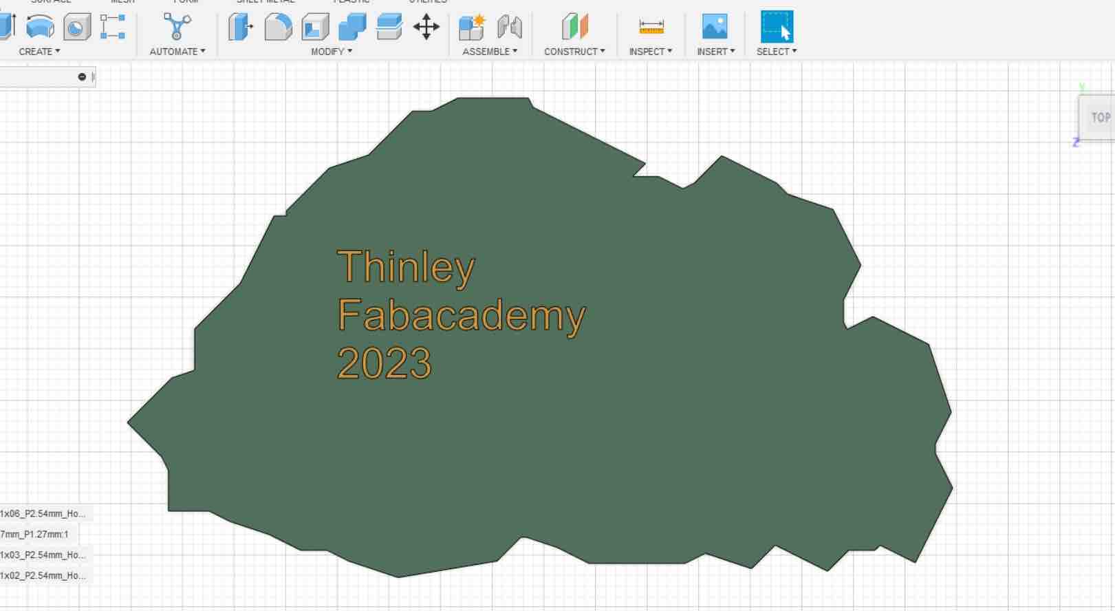
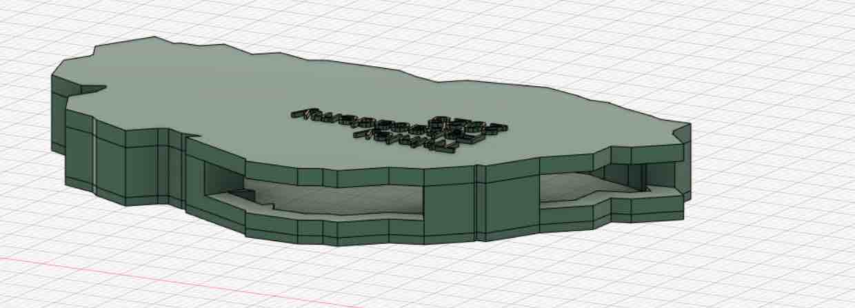
Extra: Case for the PCB
Made in Fusion 360
Design files
KICAD Files for the week DESIGN FILES