Electronics Design and Production
Planning
I’ve come up with two plans and the electronic diagrams for both and will also be finishing up the electronic mcu design this week.
Plan 1:
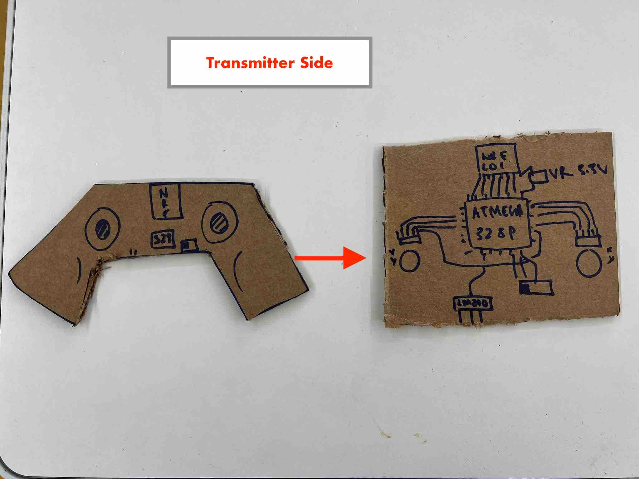
Plan 1 entails creating my own AtMega328p board with the NRF module for the transmitter and then using off the shelf arduino for the receiver side on the drone (If making the receiver board takes too long).
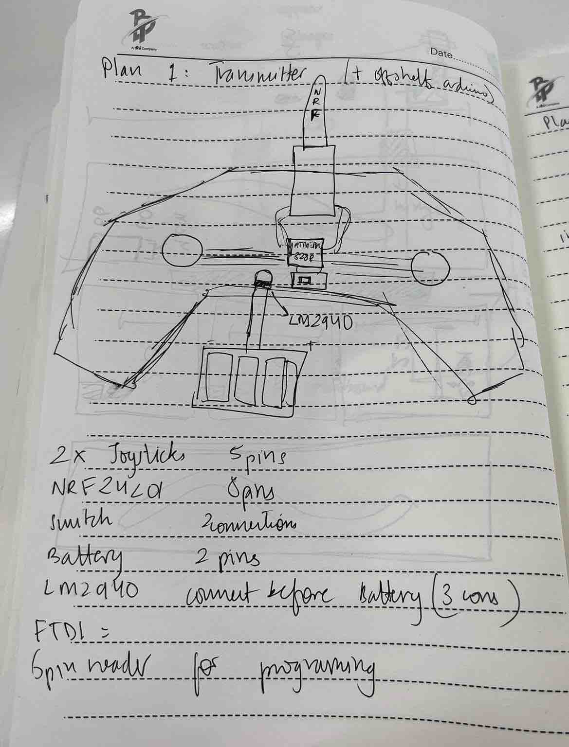
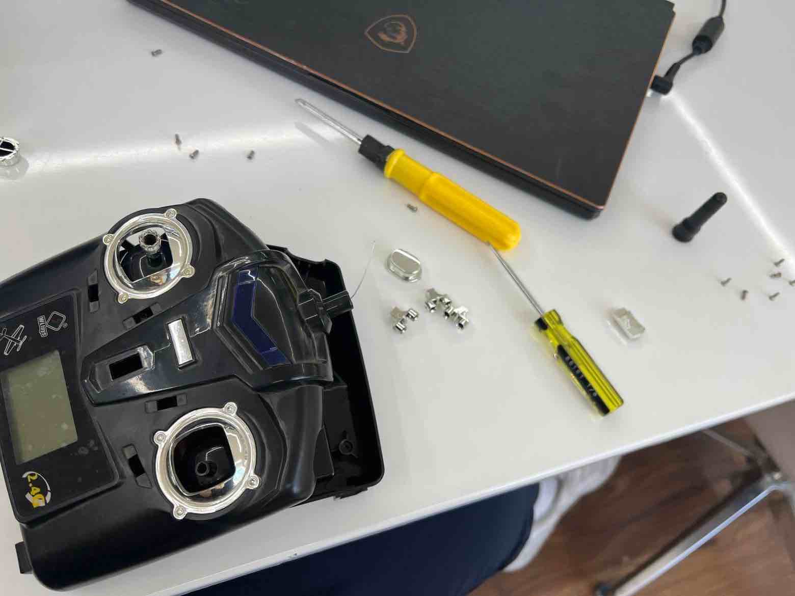
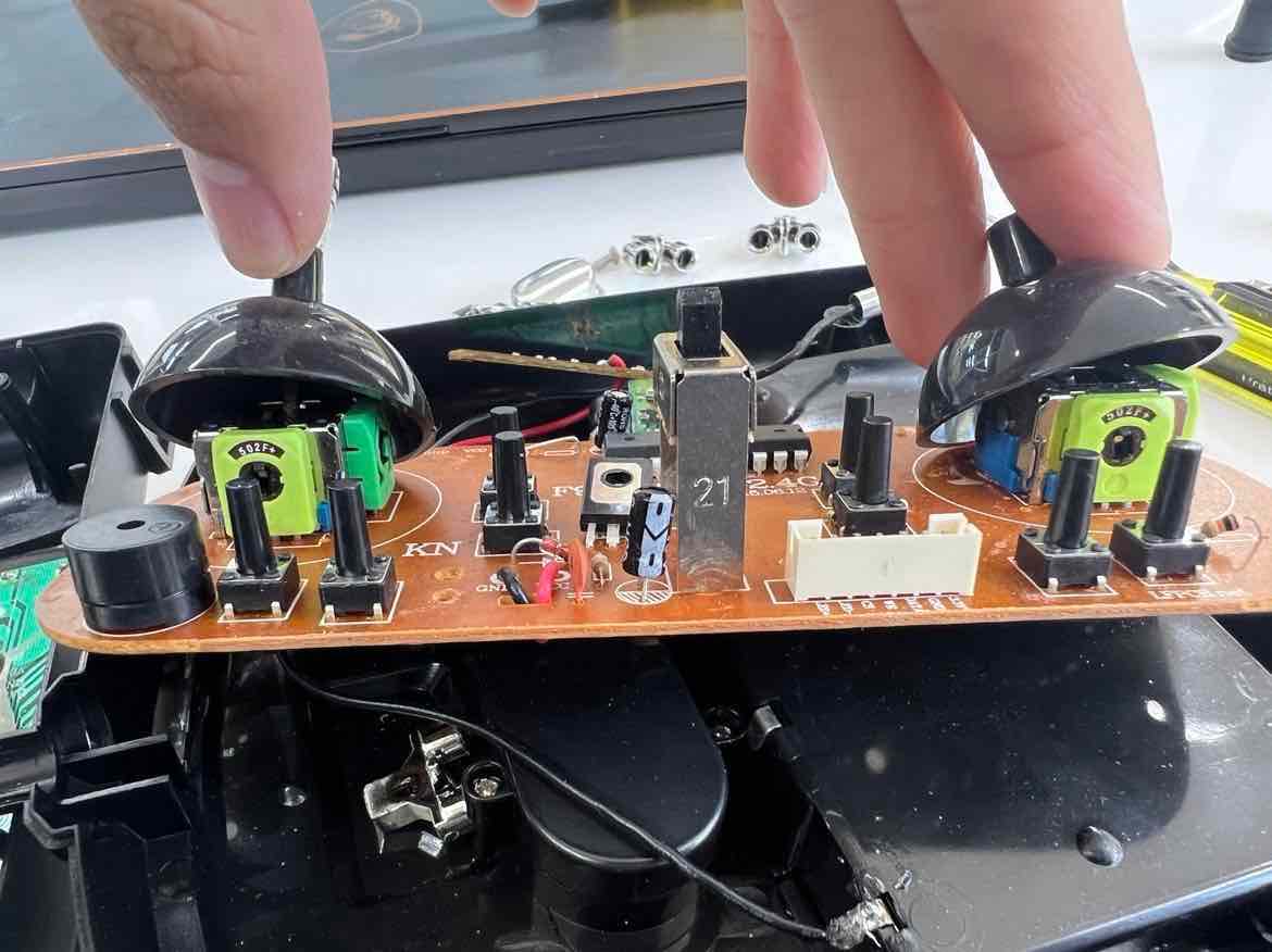
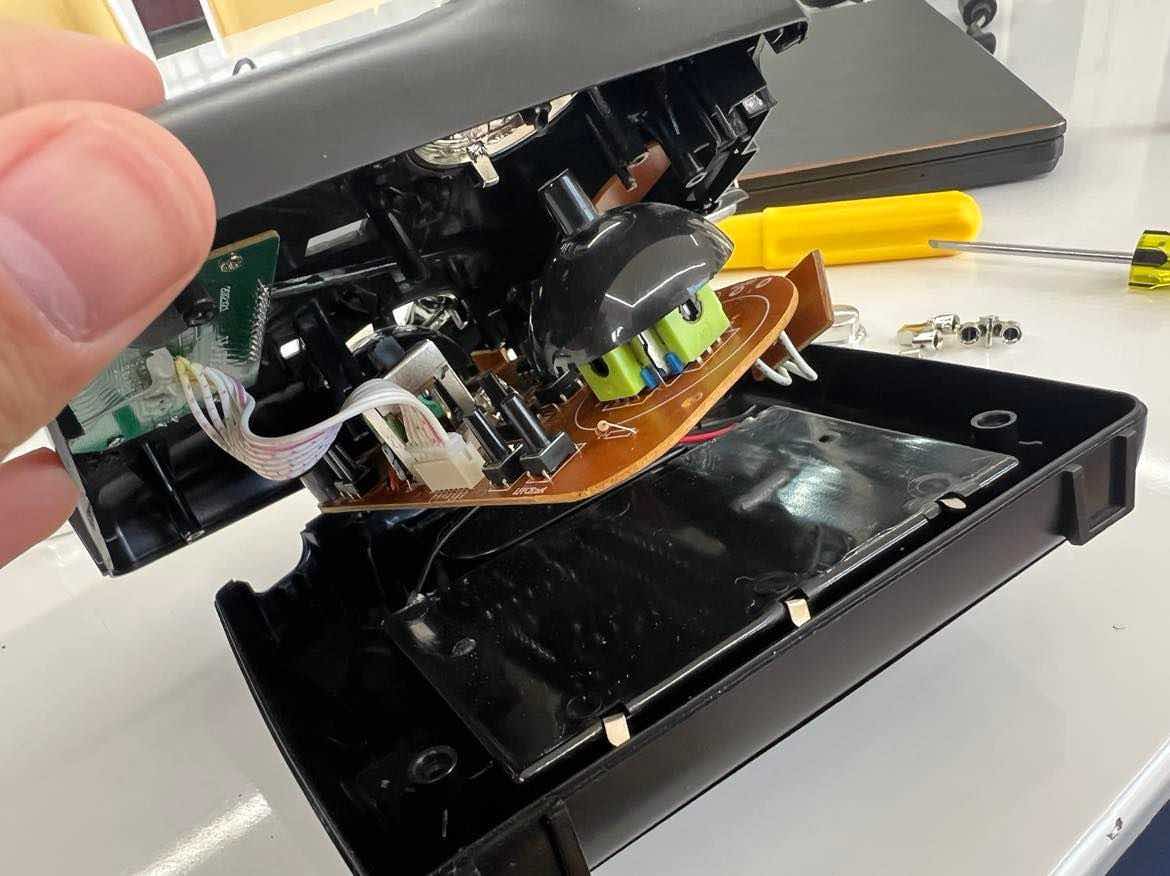
since we do not have joysticks in our lab, I have been trying to pry open an old transmitter system to study it and to get ideas from it.
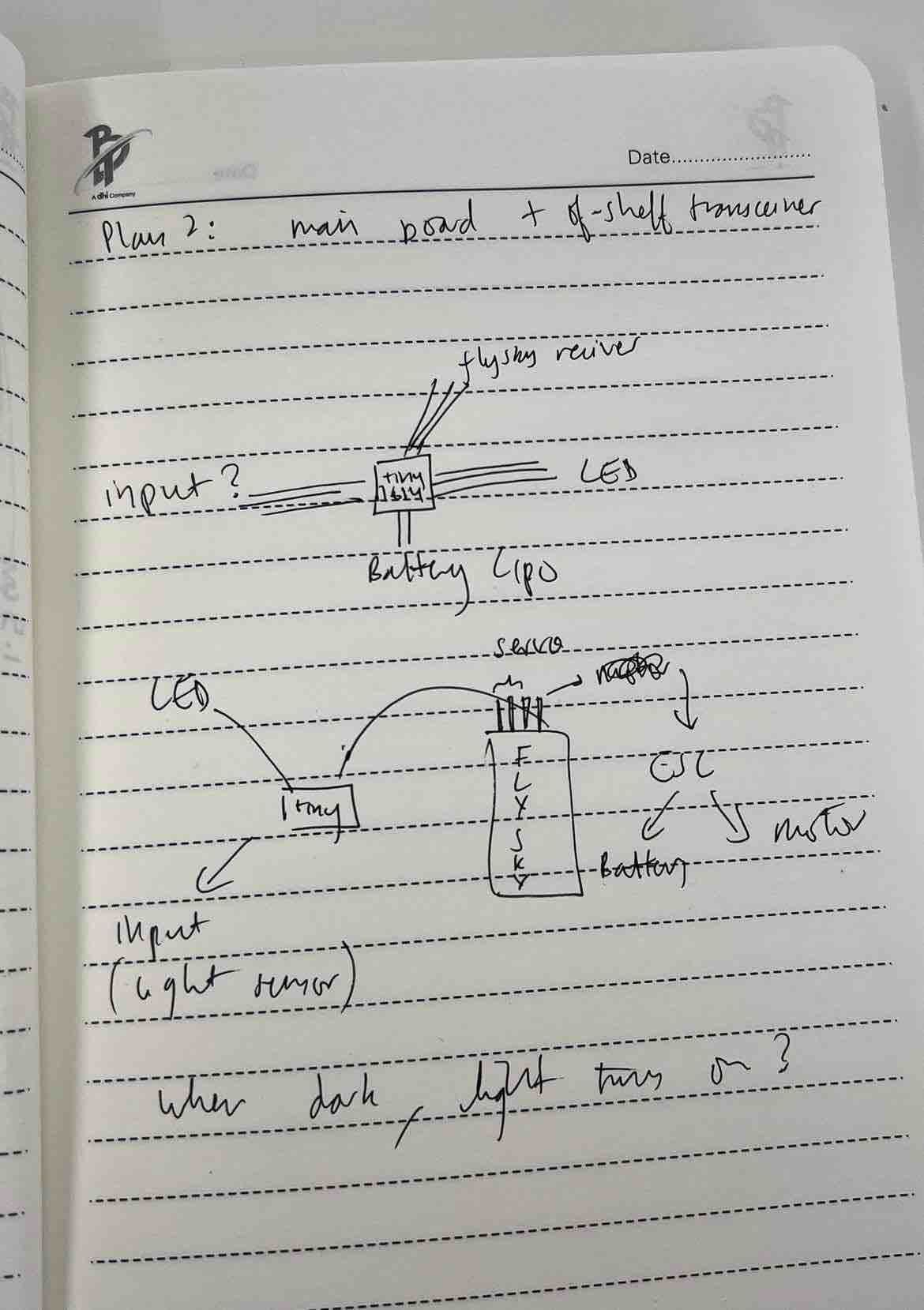
Plan 2:
Plan 2 would be to not worry about the transceiver but to use flysky’s off the shelf transceiver that, will connect to a attiny1614 board. The board will have an input like a light sensor and output of LEDS, so that the drone will auto lightup once its dark.
Beginning electronics design (TRANSMITTER):
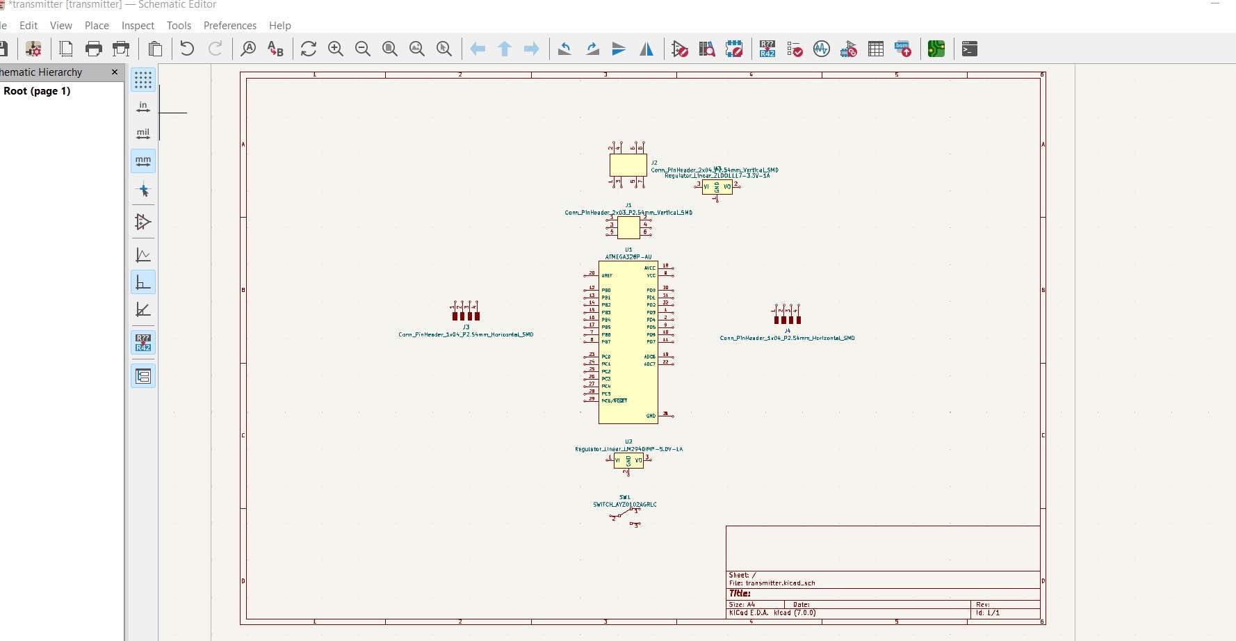
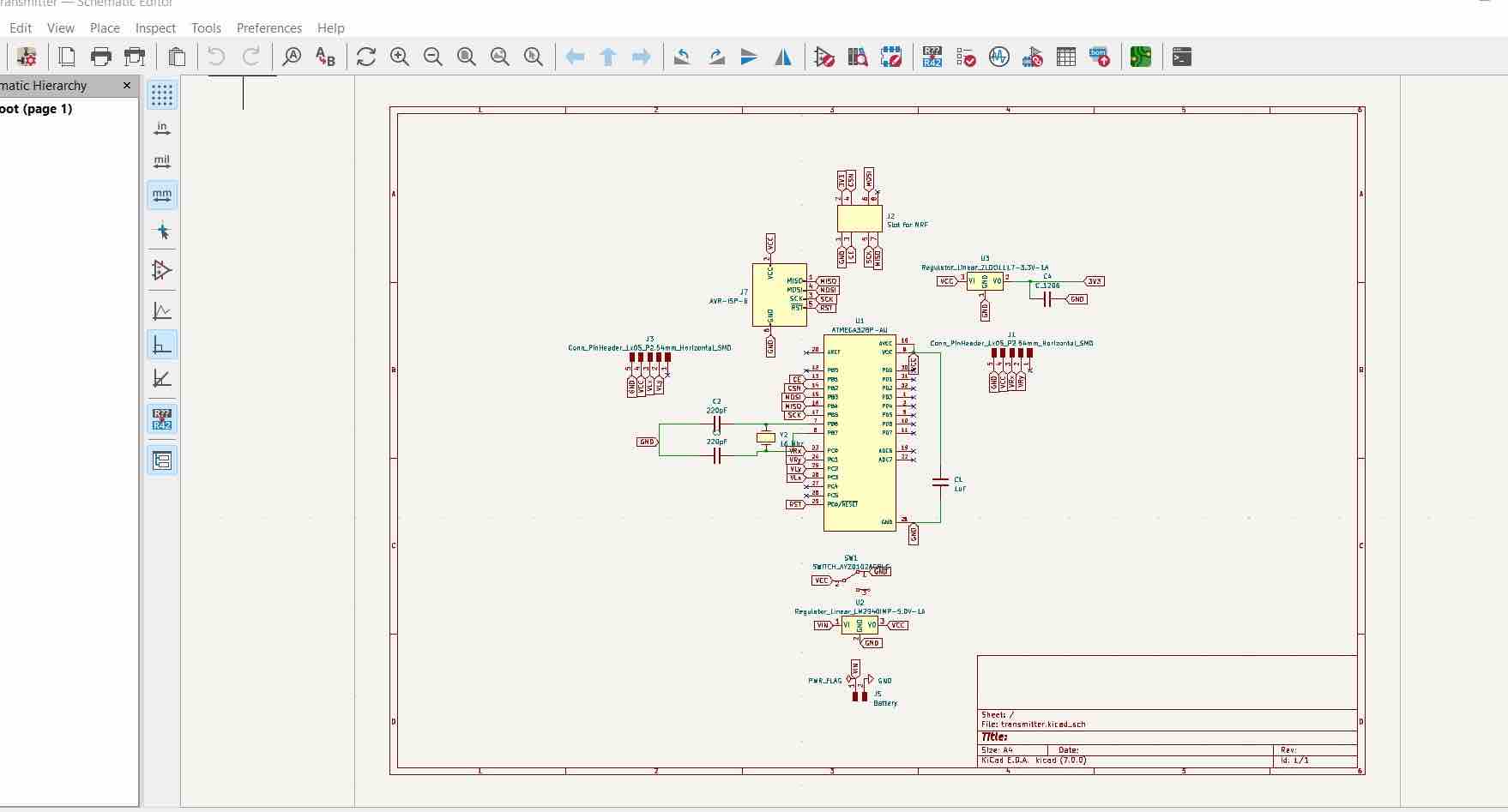
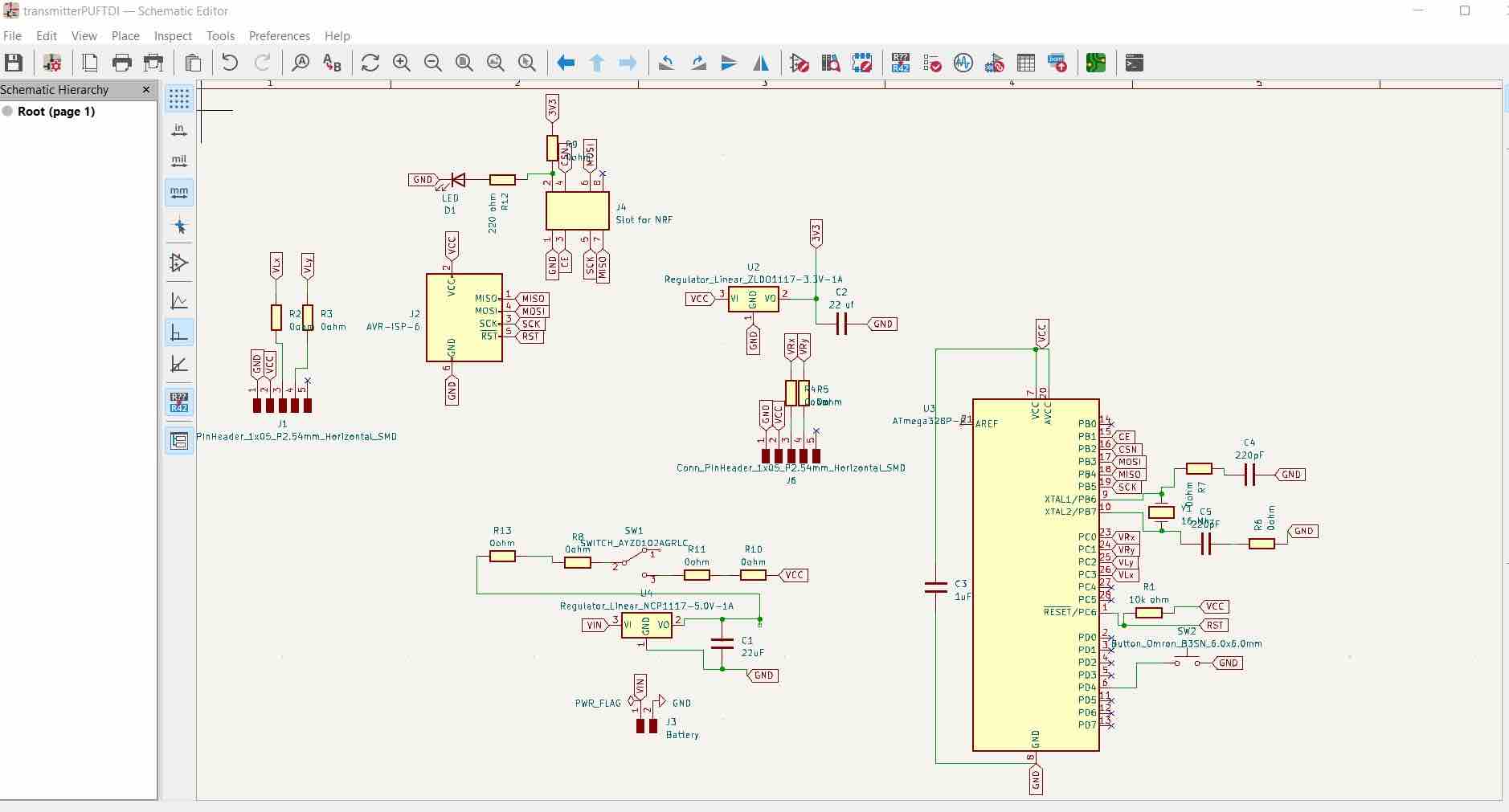
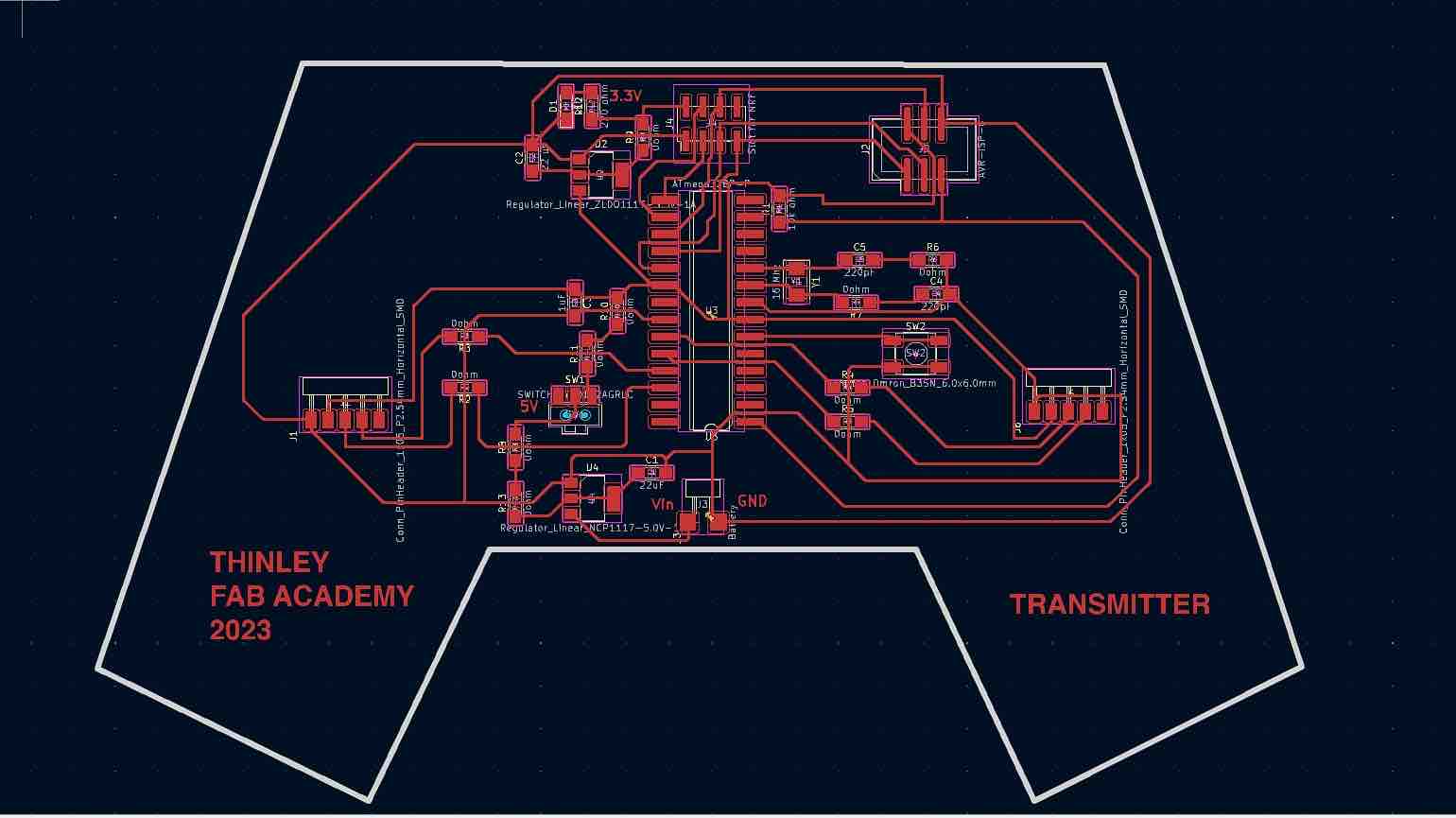
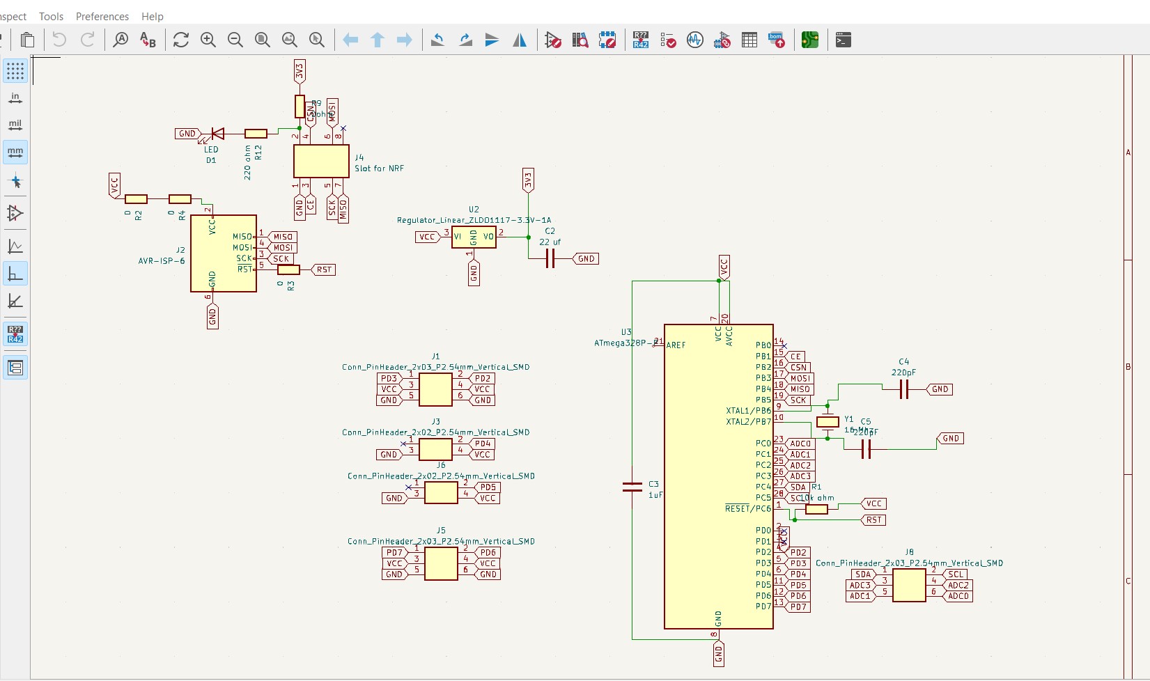
I had to spend quite a lot of time doing research to figure out how to design and fab my transmitter’s board. After that, I began putting listing together my components in KiCAD.
In KiCAD, I realized that I did not have the Atmega328p-AU symbol and footprint so I had to download and install it from SnapEDA. Atmega328p-au link. Once downloaded it needs to be brought into Kicad. To do this,
first in the Schematic editor:
- go to
preferences manage symbol libraries- click on the
foldericon on the bottom left - select the newly downloaded sch file (inside the folder) from SnapEDA
- hit ok
then, in the PCB editor,
- go to preferences
manage footprint libraries- click on the
foldericon on the bottom left - Select the newly downloaded folder from SnapEDA
- hit ok
Im still figuring out how I will connect the battery to the board but here is the current progress:
Update:
Excruciatingly, I had almost completed my the SCH and pcb design in KICAD, when I was informed that all the Atmega328p-AU’s were used up and out of stock in our lab. It also takes about 2-3 weeks time for things to get shipped here so I decided to use the ATmega328p-PU which is unfortunately a through hole mcu and I have never really worked with through hole components.
Where was progress was:
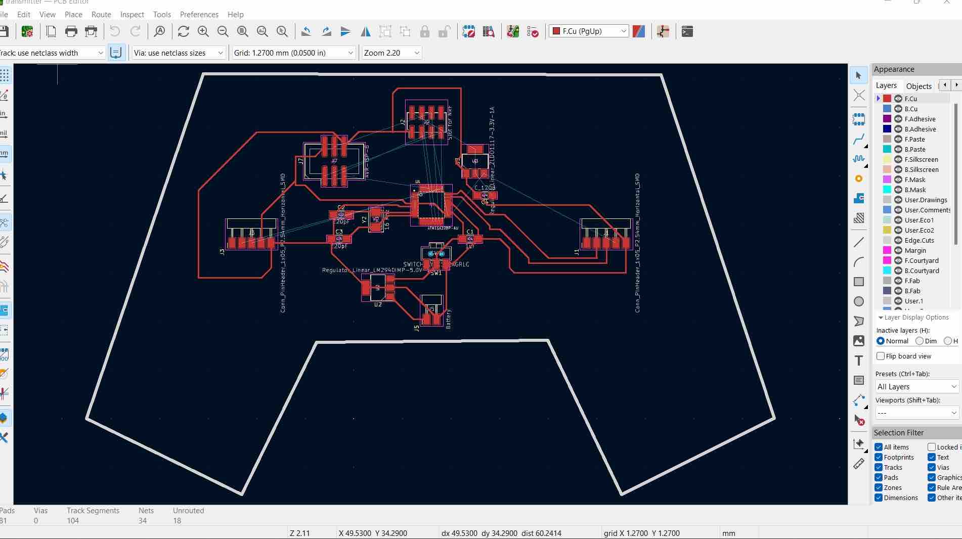
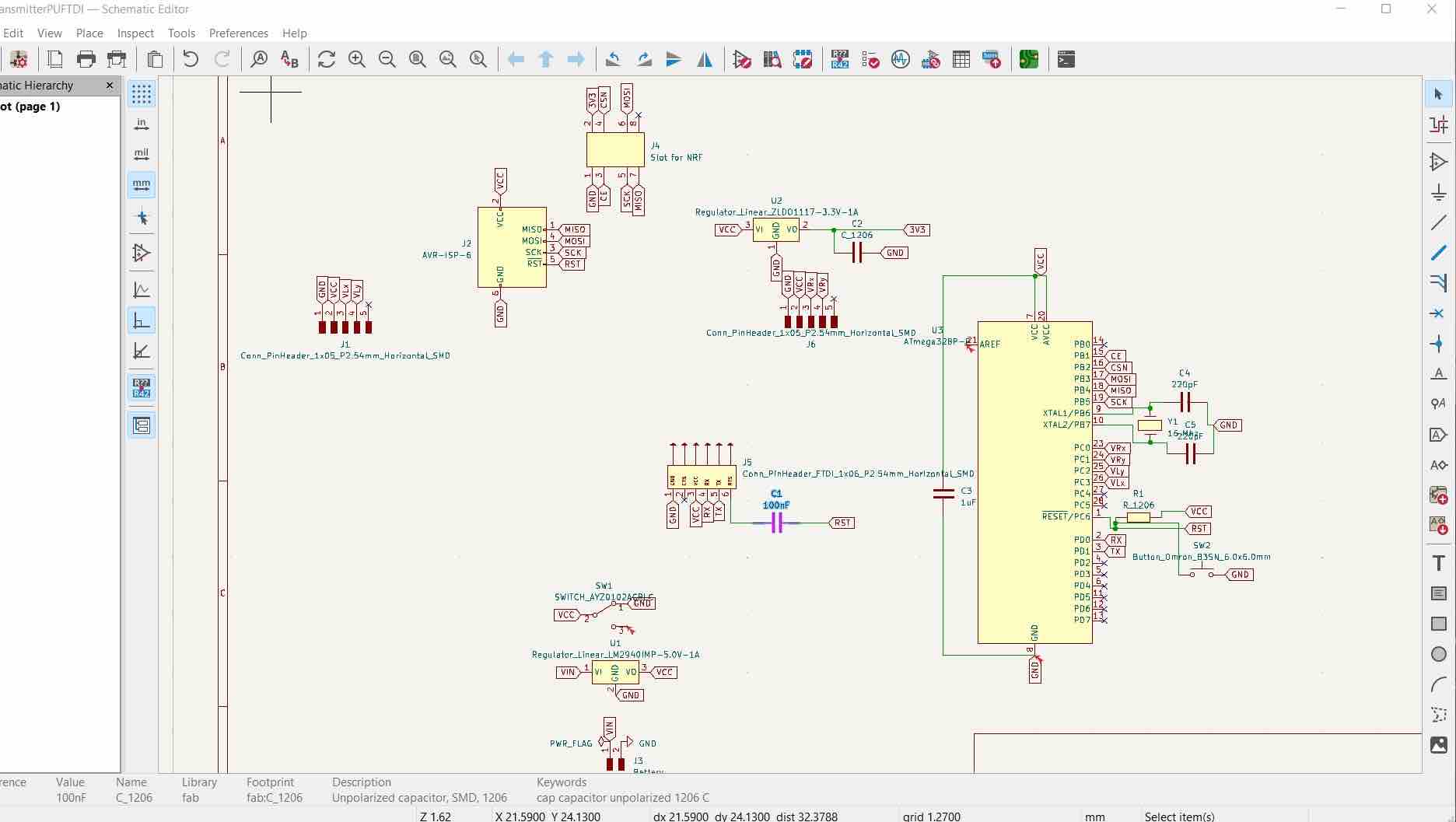
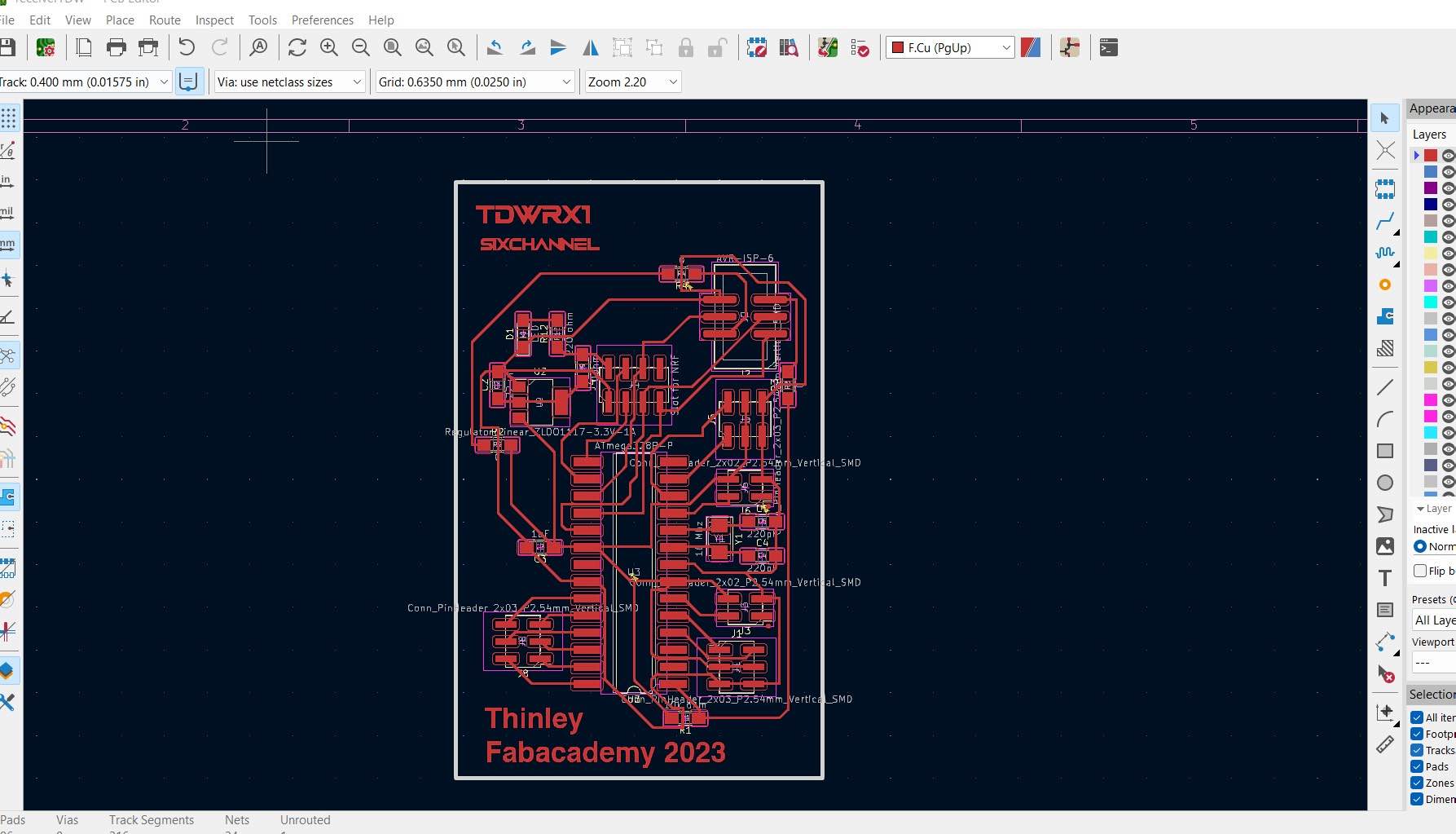
So then I had to go back, do some more researched and redesigned the electronics. I finished the schematic and am now figuring out the PCB design:
Custom Footprints:
The ATMEGA328PU in the lab is a through hole component. I have not really worked with through hole components, plus I would have had to solder the component on the bottom side of the copper since all the other components are SMD.
So if I wanted to uses the PU as a SMD component, I had to gently bend the legs of the PU first, and then make my own custom footprint. To do this:
- First I took the already existing PU through hole footprint and copied it.
- Then I
right-clickedon an individual pad and went toproperties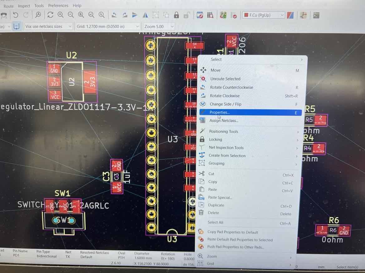
- Then I changed the pad type to SMD
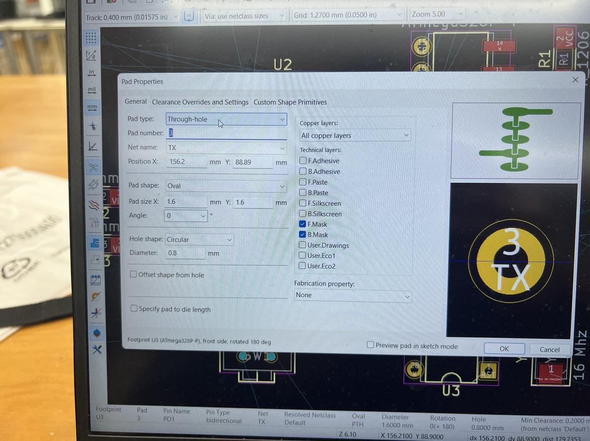
- Then I changed the Pad shape to Oval and resized the Pad.
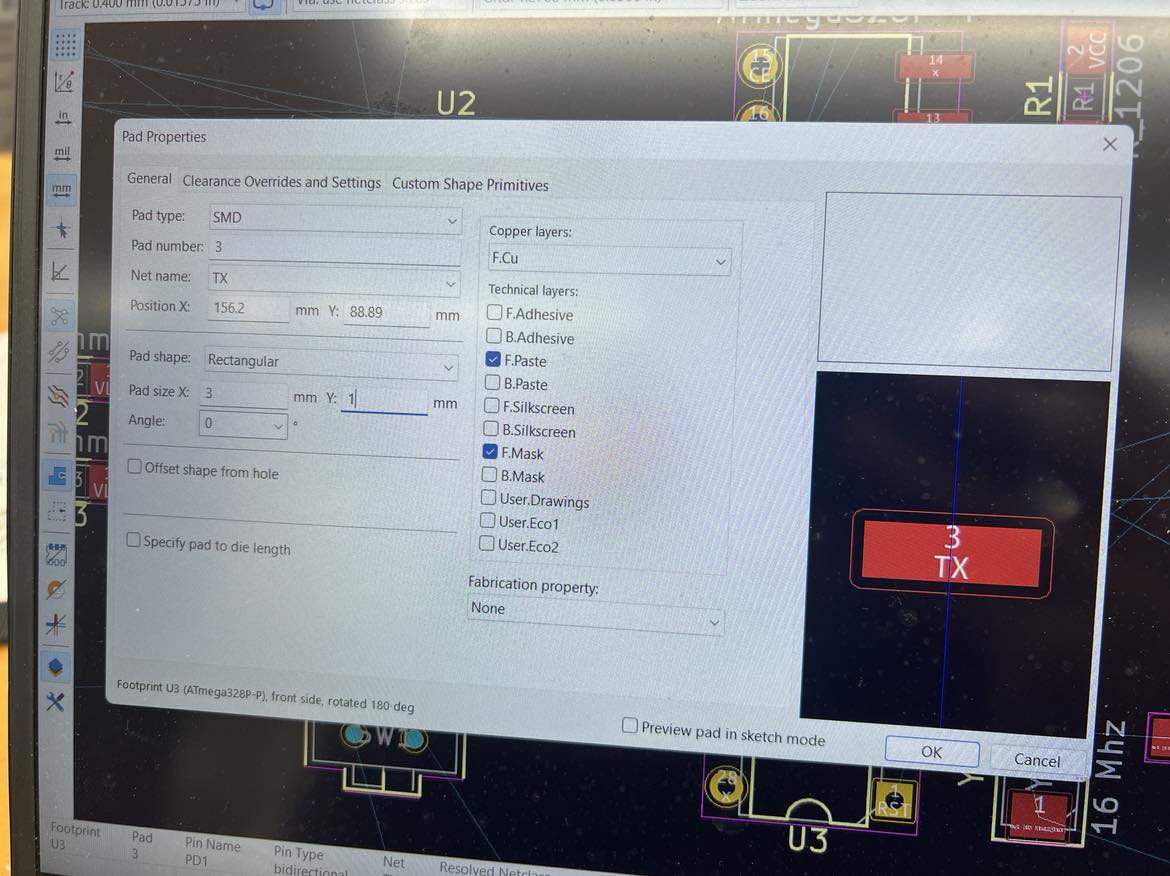
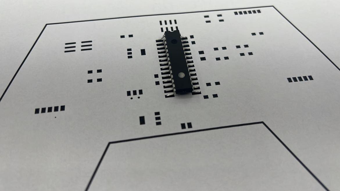
- The resizing and pad position is a bit tricky, since the legs will have to be bent, so I took Rico’s suggestion and printed out my PCB on paper to check how it worked and how much I had to edit it. It took me three tries to get to where I wanted. Final sizing:
- It’s a bit of an hassle to have to right click all the pads to edit it, so a nice trick is to edit just one pad, and then to right click said pad, and then hit ``Push Pad Properties to other Pads”.
BOARD 1 and 2
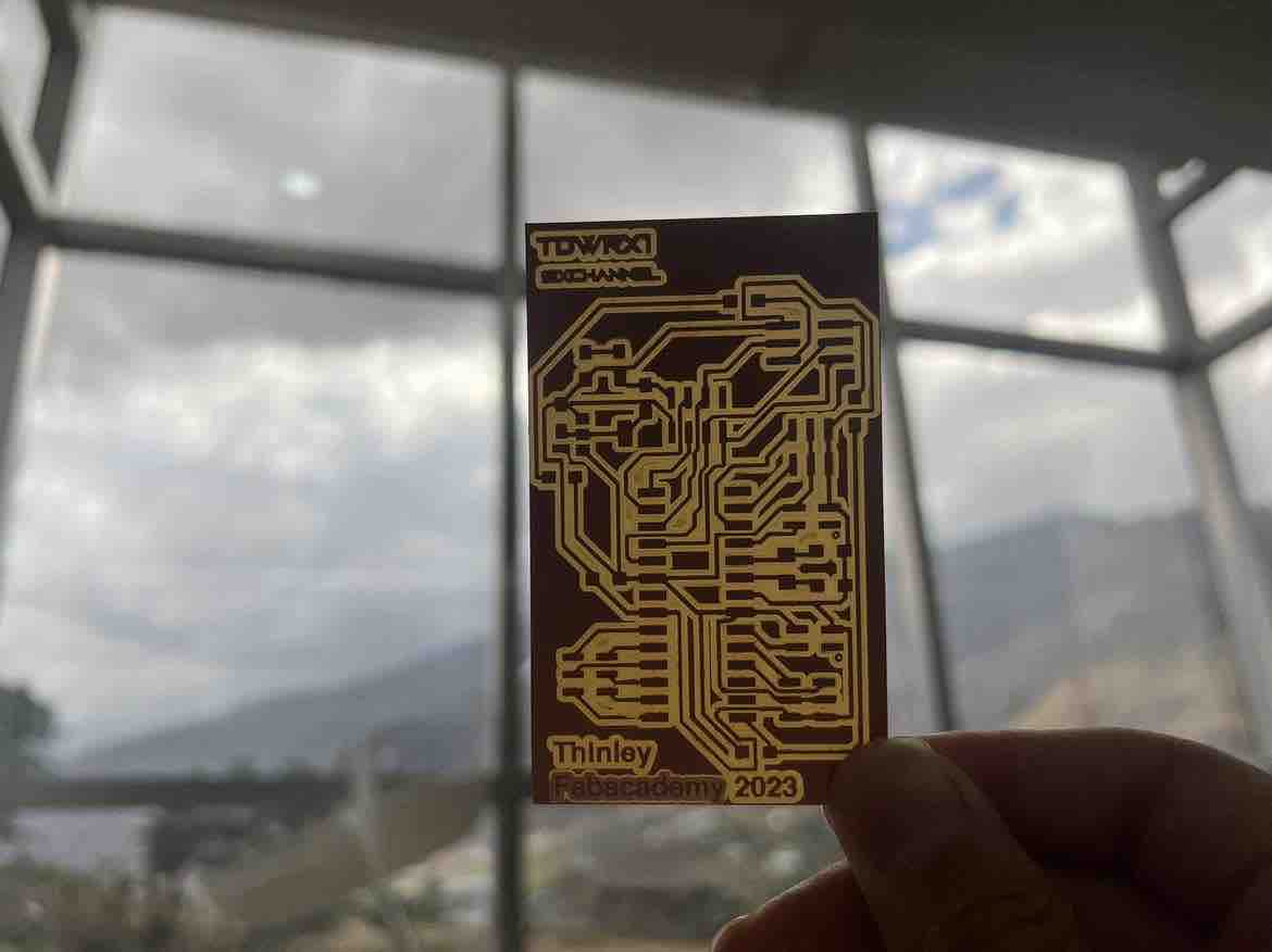
I After completing the board design, I went ahead and milled board. The First time, I forgot to customize net classes and forgot to add constraints to my design so a lot of my tracks overlapped pads. This is definitely not good so I went back, added custom net classes and added proper constraints and clearances to my design (Design rules).
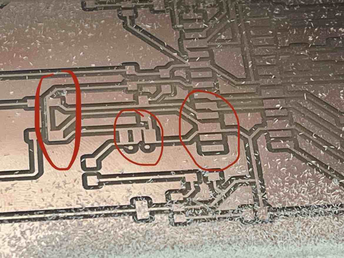
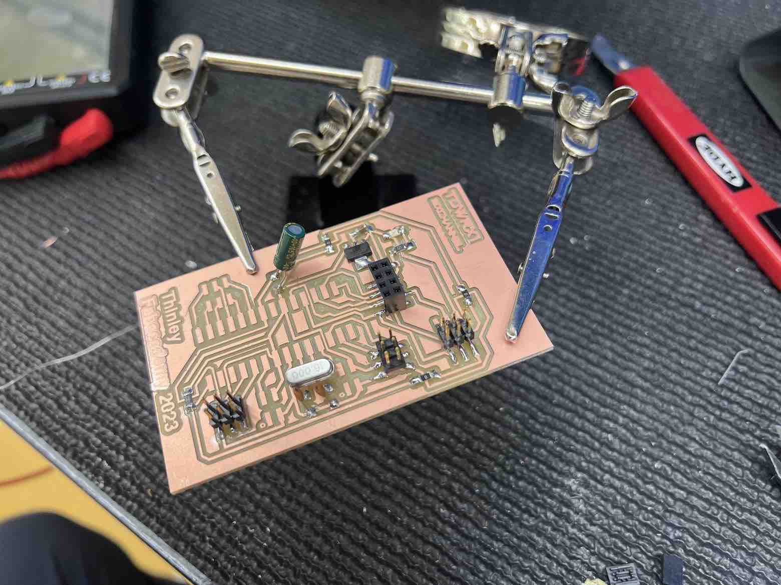
I milled my new board and soldered all the components except the mcu (atmega328 PU). As soon as I powered my board, the 5V regulator starting heating up which meant it was shorted.
Upon debugging, I made a careless mistake of not checking to ensure that the footprint was proper and ended up using LM1940’s footprint rather than the NCP117 (datasheet here). I went back to the drawing board, changed the footprints and confirmed the footprints for the rest of my components as well. I also added a LED to the 3.3v supply to the NRF.
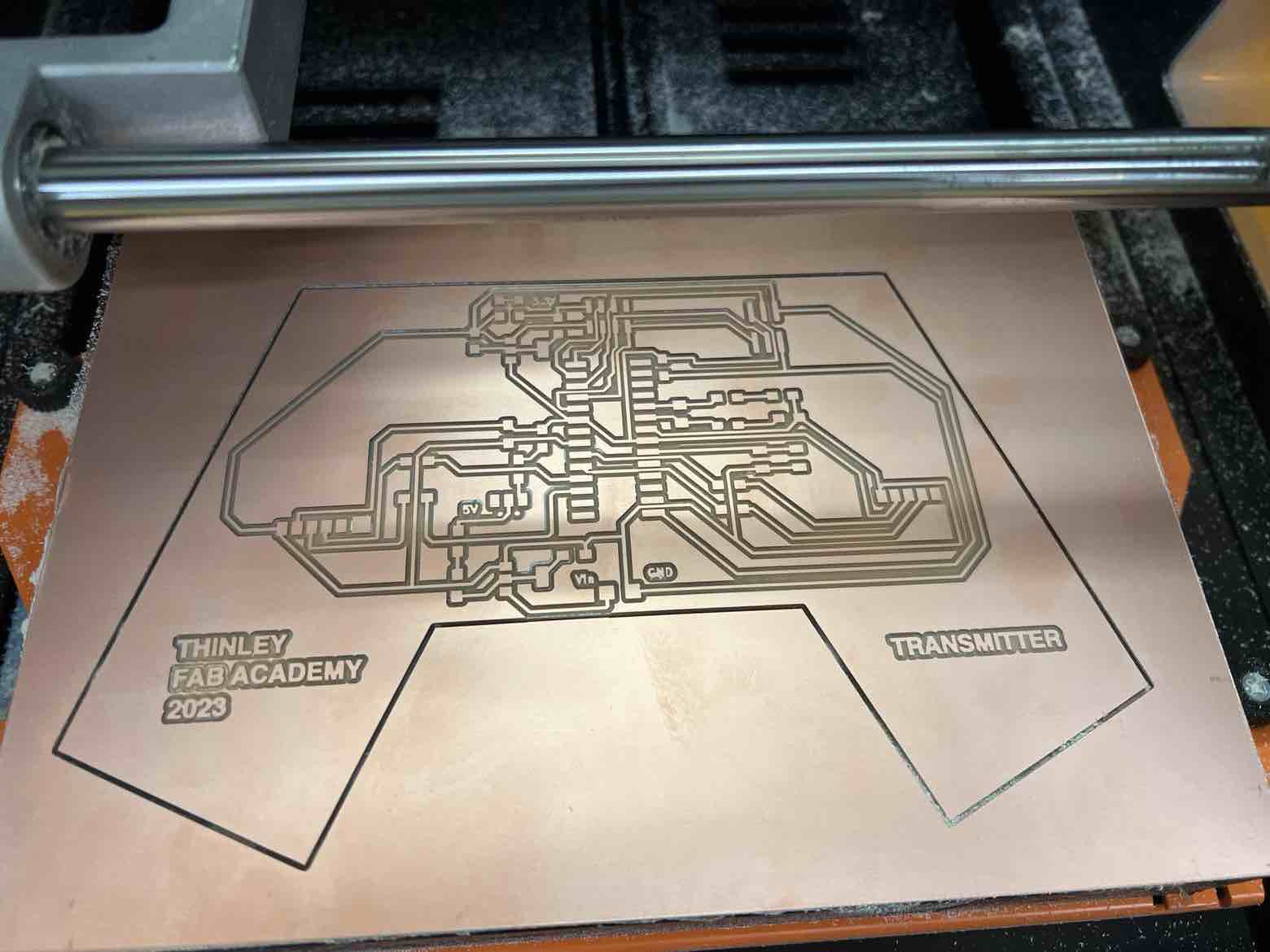
Then I re-milled the board and soldered the components on to it, first testing the voltages before soldering my MCU, and it worked! Both the 5V and 3.3V regulators did there job.
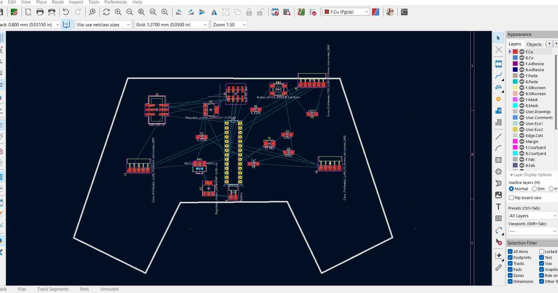
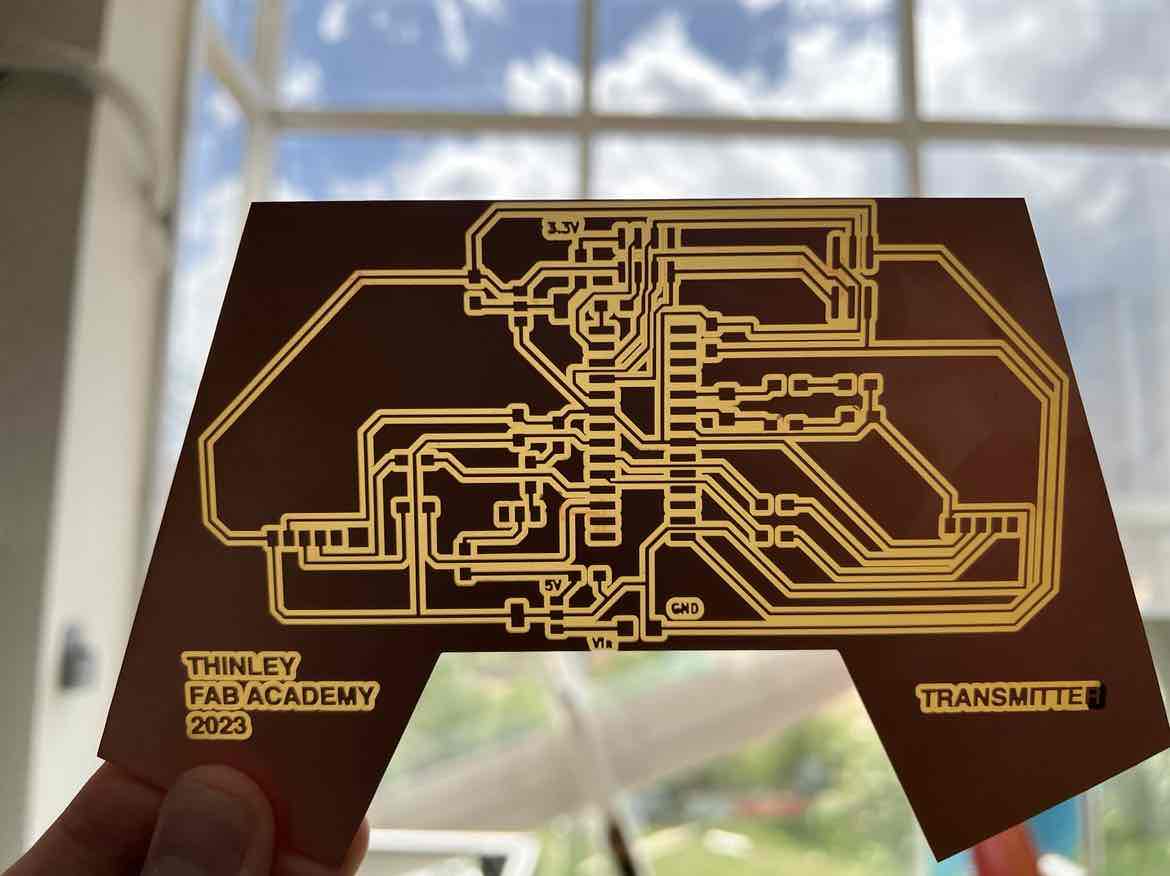
The Final Schematic and PCB:

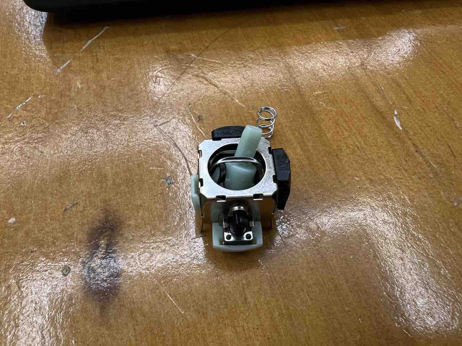
Happy, I soldered on my mcu as well. I also de-soldered the joystick’s connection pins and re soldered them upside down for proper accessibility to my board.
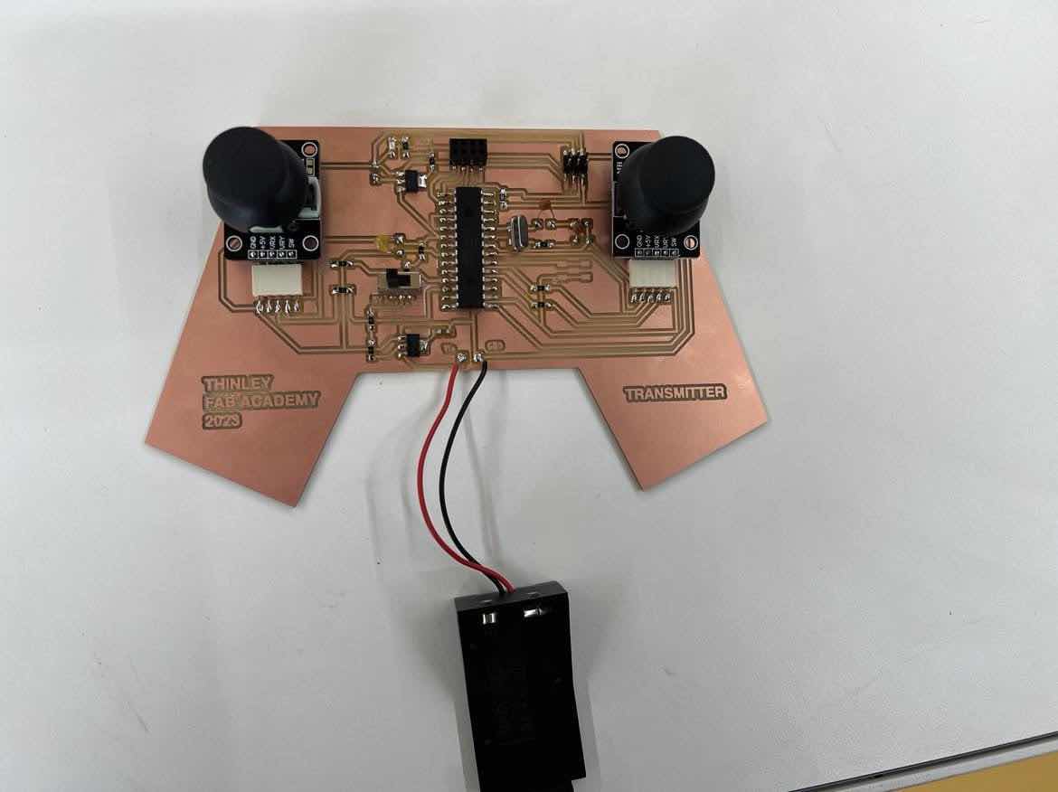
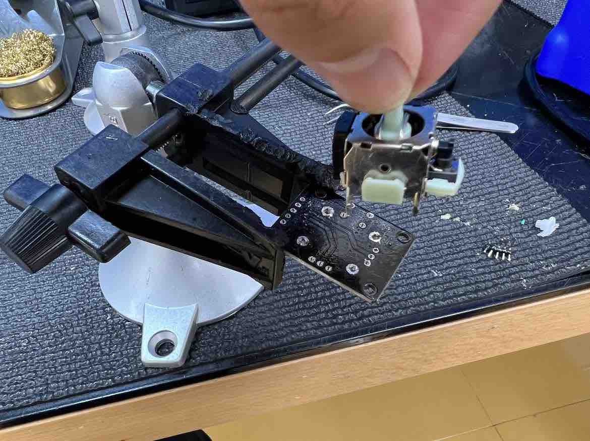
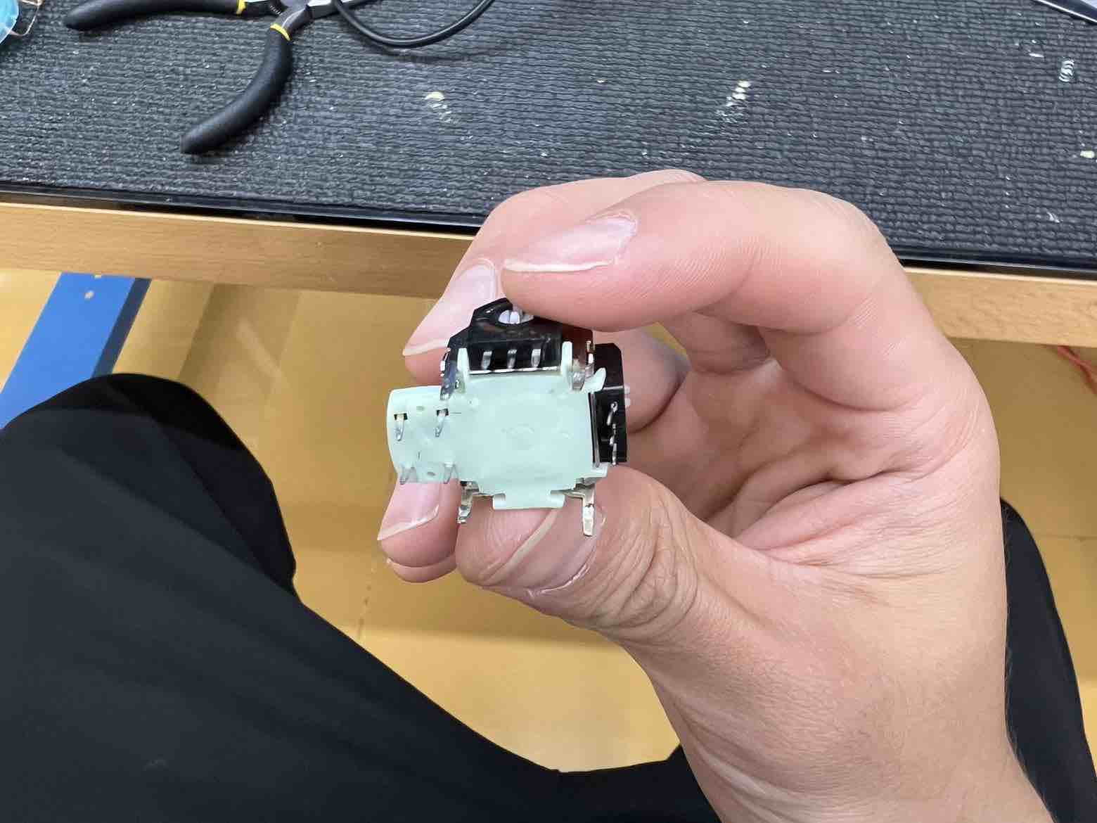
After some testing, I removed the spring inside the left joystick for a more “Drone joystick” feel. I desoldered the board of the joystick, then removed the plastic tab holding everything in. Then I removed the spring that brings the joystick back to the center. This was very time consuming but well rewarding.
NRF Module Connection:
The pins on the NRF:
GND, VCC (3V3), MOSI, MISO, SCK, CE, CSN.
The connection of the NRF Pins to my Board:
GND: GND VCC(3V3): 3V3 From Regulator MOSI: D11 MISO: D12 SCK: D13 CE: D15 CSN: D16
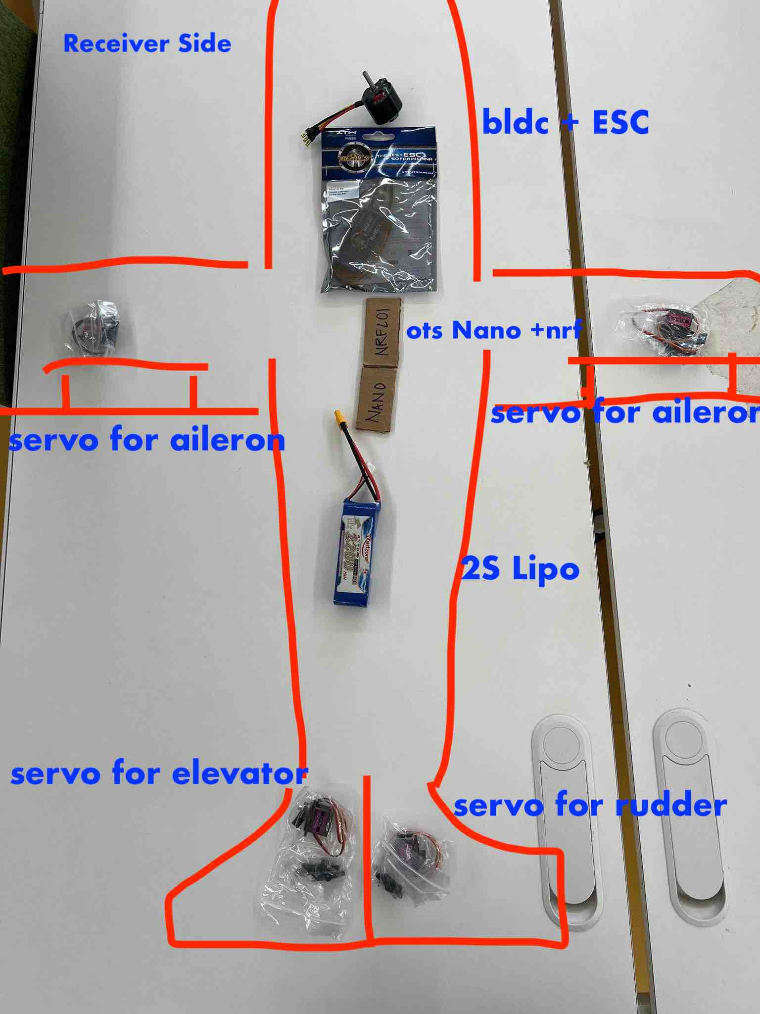
Receiver Electronics:
For spiral 1, I wanted to focus on making my own board for the transmitter, while I use an Arduino Nano Every with prototyping pcb for the receiver to save time.
For this, my main reference point was this amazing video: DIY 6 Channels Radio Control
I first soldered female pins which would hold the nano every on the prototyping pcb, followed by the NRF24L01 module.
I followed this schematic (from the above user):
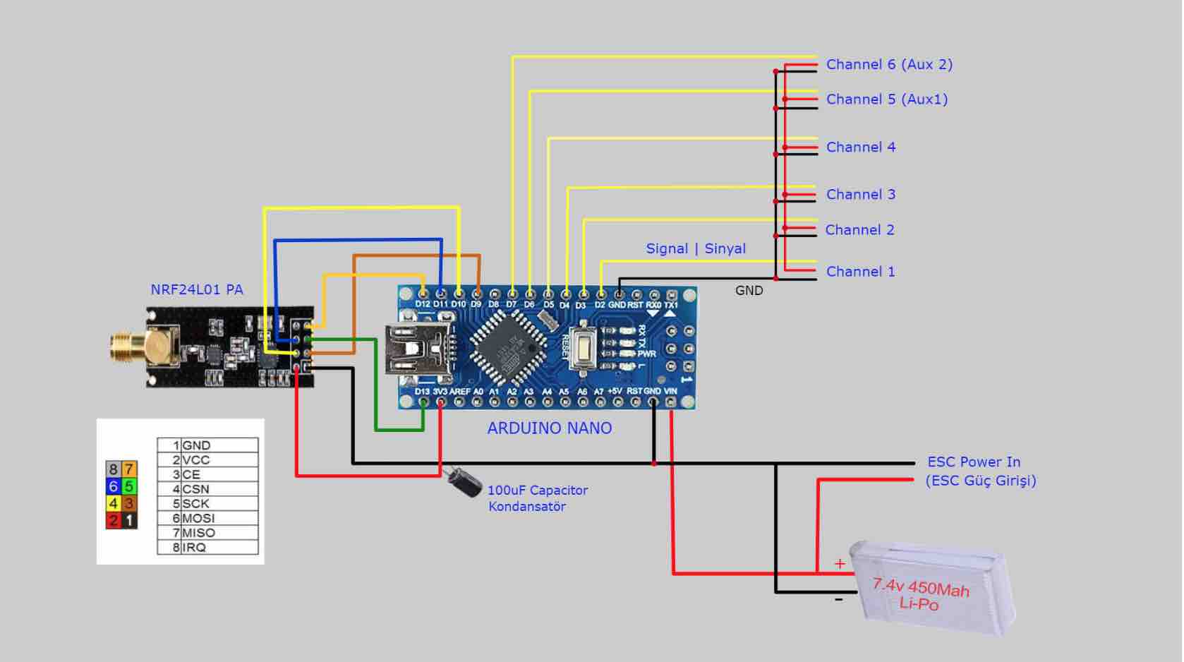
The biggest change is that I will be powering my entire board using the Electronic Speed Controller’s in built BEC whereas most people connect the LIPO directly onto the board.
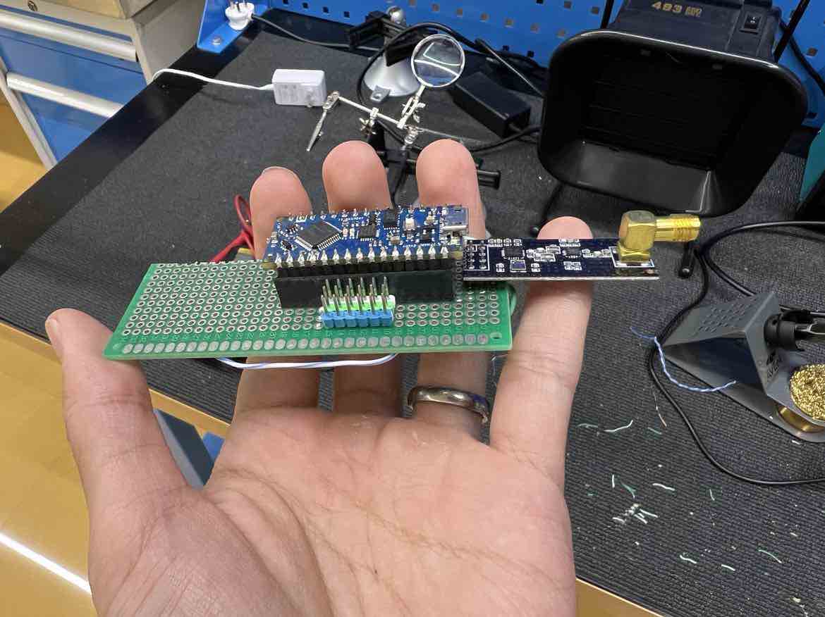
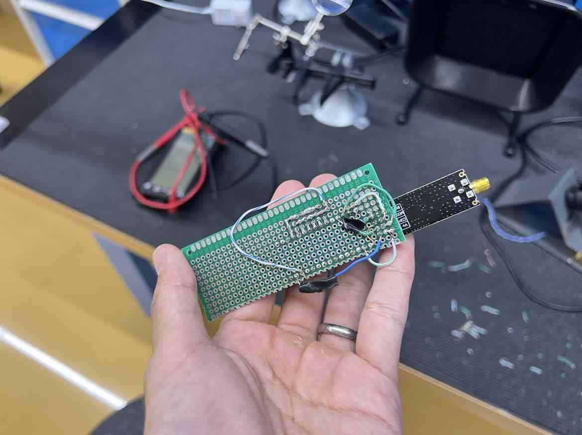
As you can see, I used regular wires to make the soldered connection between the components. I was also successfully able to program the Receiver. I did have to manage boards in the Arduino IDE and download the megaAVR board libraries so that I could select the board to be the Arduino Nano every.
Electronics Spiral 2
While working on my 3D design, I also decided to work simultaneously on my custom Receiver board based on the Atmega328PU, just like the Transmitter board I made.
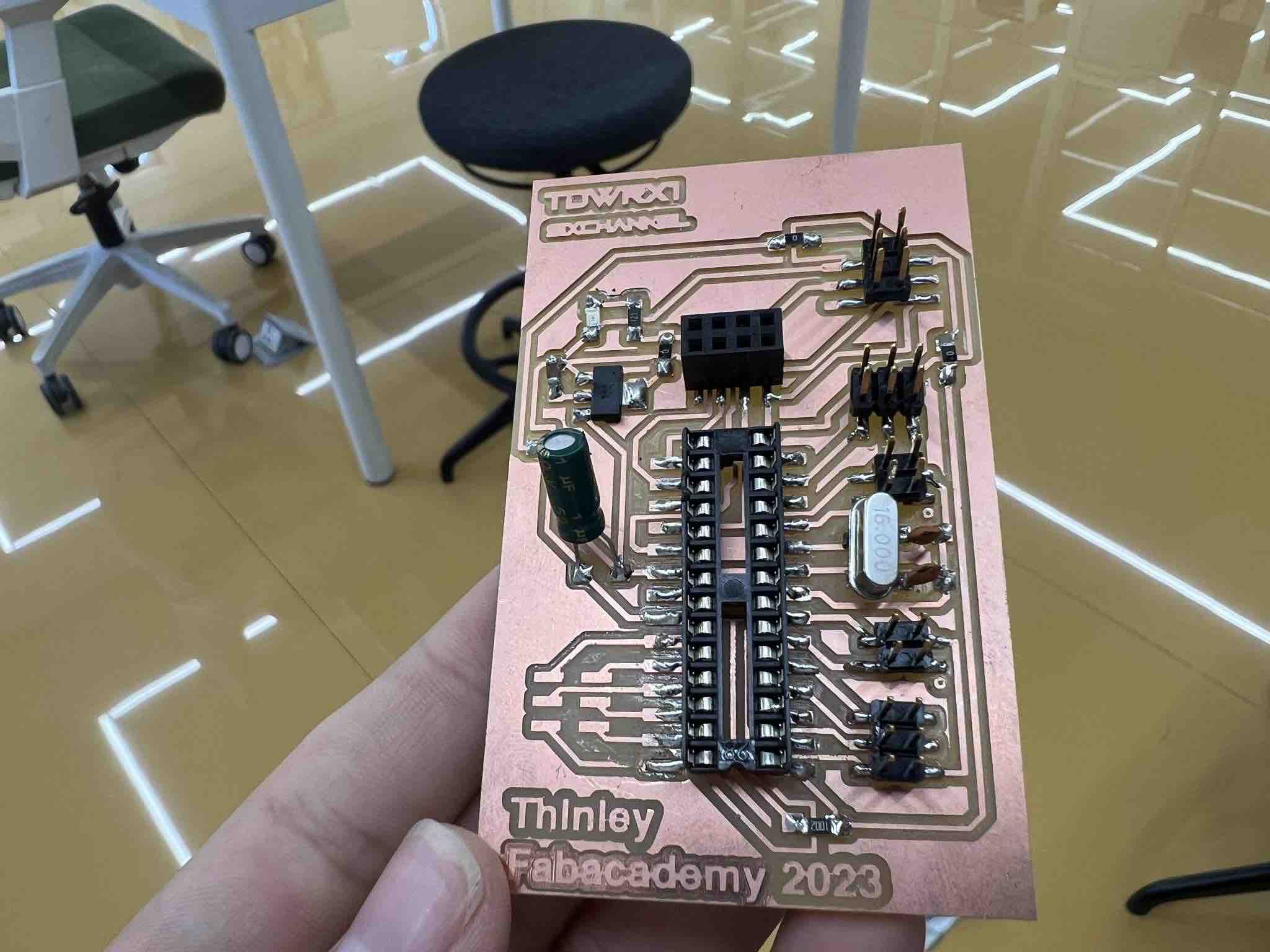
My first version of the RX board:
I went ahead and Milled on the Roland SRM20:
And then Soldered all the components:
Final board with the MCU holder:
testing can be found in Programming.