7. Electronics Design
- Study Plan
- Research / Group Assignment
- Individual Assignment
Assignment definition
Group assignment
use the test equipment in your lab to observe the operation of a microcontroller circuit board
Individual assignment
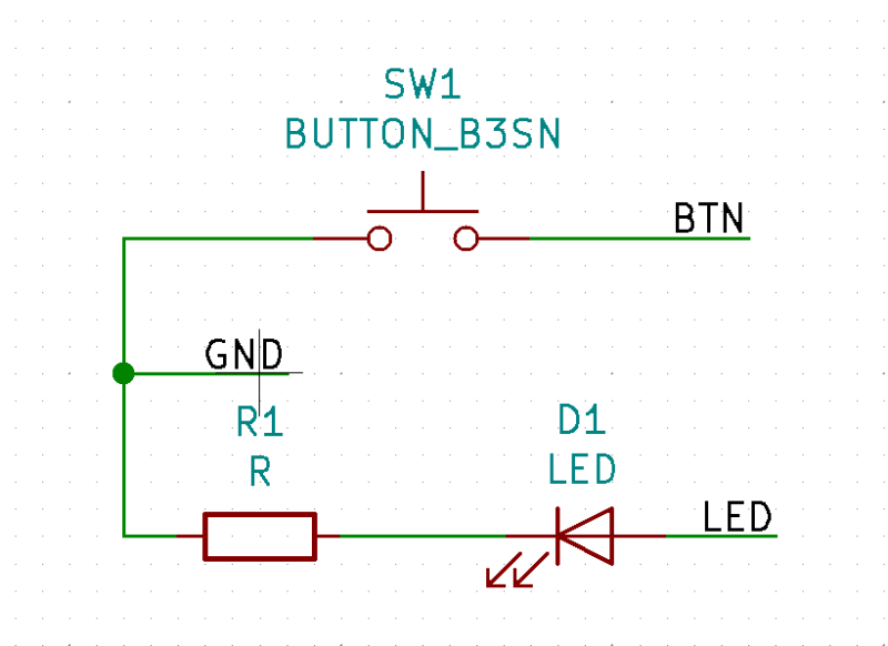
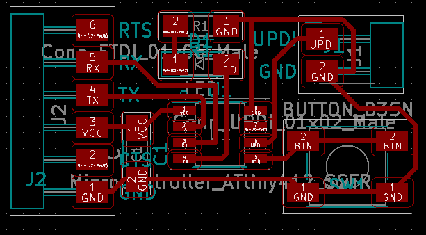
redraw an echo hello-world board, add (at least) a button and LED (with current-limiting resistor) check the design rules, make it, and test it extra credit: simulate its operation
| This week I wanted to | Result |
|---|---|
| Learn KiCad | Done with the tutorial of Kris |
| Use the test equipment to analyze a microcontroller | Done with Maxime, we decode SPI and compared analog and digital signals |
| Redraw a hello board : AT Tiny 412 with a LED and a button | Done Friday thanks to the tutorial of Kris |
| Redraw the programmer board : CMSIS-DAP.4.D11C | I did not do that but I produced the one that Maxime drew |
| Install end course sensors on my 3018 CNC | Not done |
| Simulate my circuit using Spice | Not done |
| Learn to use my 1810 CNC to make my own circuit board | Discussed with Dan during the Global Open Times |
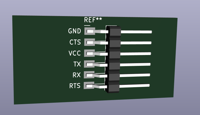
| Design and produce a header converter 1.27mm to 2.54mm|Done on Saturday| | Add videos to my website|| | Add 3D files to my website|| | Rework the previous assignment pictures||
Study Plan
| Day | Activity |
|---|---|
| Wednesday | Course with Neil Gershenfeld |
| Thursday | Group Assignment + Plan project & Individual assignement |
| Friday | Learn KiCad + Mill & Assemble circuit |
| Saturday | Global Open Time + Design 1.27 to 2.54mm converter |
| Sunday | Break |
| Monday | Produce JTAG Programmer & Start Final Project v0 |
| Tuesday | Complete documentation |
Group Assignment : Analysing a microcontroller behavior
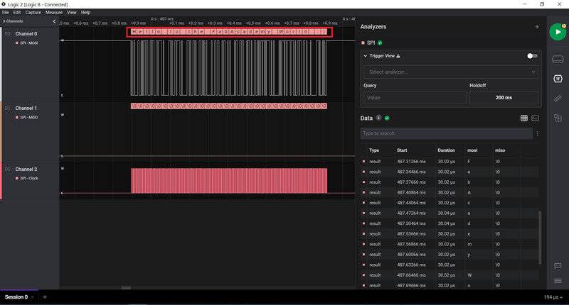
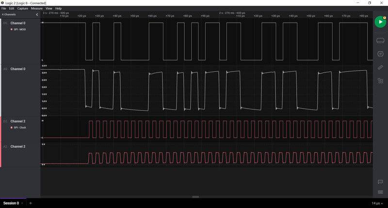
We analysed the microcontroller outputs using Maxime’s analog-digital analyser which is a very powerful device to analyse microcontrollers.
The sampling frequency is very high (50MHz) but the voltage range is limited to 5V. It has 8 channels which makes it a great tool especially because it only cost 400 € and fits in your pocket.
It is thus appropriate and powerful for microcontrollers analysis and low voltage circuit analysis but not for higher voltage circuits.
Another advantage is the fact that it’s a digital and analog analyser so it does both jobs simultaneously.
I later got myself a similar very cheap one on Amazon that works great with the software of Saleae .
We documented it in details on our group website.
What we had the most fun with was the telecommunications decoder, decoding directly in the digital analyser software and the comparison between real analog signals and the digital ones.
Individual Assignment : Designing a circuit board
I covered mostly practical design as for the physical part of electronics I have covered during my engineering studies.
Learning KiCAD and Electronics Design
I wanted to learn KiCad with this video French Tutorial of KiCAD 5.1.6 But it is too long even if it goes in length on how to design pieces from start to finish.
Thus I followed the KiCAD tutorial of Kris from Fablab Aalto
Shortcuts in ciruits : Eeschema
- W to place a wire
- M to move a component
- R to rotate a component
- L to add a label
- Enter to place (anything like a click)
- G to grab a piece without breaking connections
The first step was to add the Fab libraries to KiCad
Then to find the schematic of the ATTiny412 that we’ll be using, Kris advised to go check this page, however I don’t know yet how I would have gotten to it on my own.
Github Ref for ATTiny412 connection
The other solution would have been to check the data sheet but it’s always super long and rarely super clear. You should always find the info in the datasheet so that’s a good thing.
PCB drawing
- D is used to edit and drag a trace
This tutorial is very interesting because its complete, from start to finish ! Let’s go through it together !
Kris Tutorial on KiCAD
Here’s my excerpt of the KiCAD tutorial of Kris from Fablab Aalto
You start by drawing the circuit in Eeschema, the schematic software included in KiCAD.
In Eeschema, you can add components connect them and check the theoretical validity of your circuit.
Before all, you should add the fab library to KiCAD. It is full of components that your lab should have.
One thing to note that was not clear to me is that you should not remove the other libraries from KiCAD otherwise you will no longer have access to simple components such as 02x02 header for example.
To do that, you need to download the library and link it in KiCAD. You can find the library here : https://gitlab.fabcloud.org/pub/libraries/electronics/kicad. Follow the instructions of Kris to connect it.
Once that is done, we move on to adding components.
The different steps we followed are :
1. Import components
Importing components is very easy, to select the tool, you click on the small triangle in the tools on the left (it is called an operational amplifier or ampli-op in French). Then you click anywhere on the screen to place a component and you can search it in the existing libraries.
/week07/TutorialKris/ChoosingComponent.png
2. Connect components
Once you have placed the relevant components, you should connect them. There are two ways to connect the components in the Eeschema.
- Put wiring : It’s easy and makes sense for simple connections but can get the schematic very messy. One big advantage is that you directly see what might be difficult to combine connections and you can directly add jumpers (null resistors) to simplify the routing by jumping over other traces.
- Label connections : To avoid the visual mess of having to many wires, a good solution is to label connections. Labeling connections means giving a name to a wire. Once you have done that, you can use this very name everywhere on the circuit and the wires with the same name will be connected.
It’s a good practice to combine both type of connections and divide your circuits in blocks that are wired together and connected between blocks by labelling.
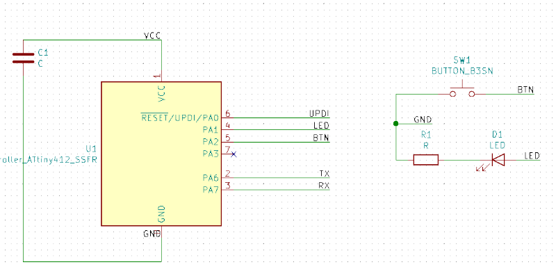
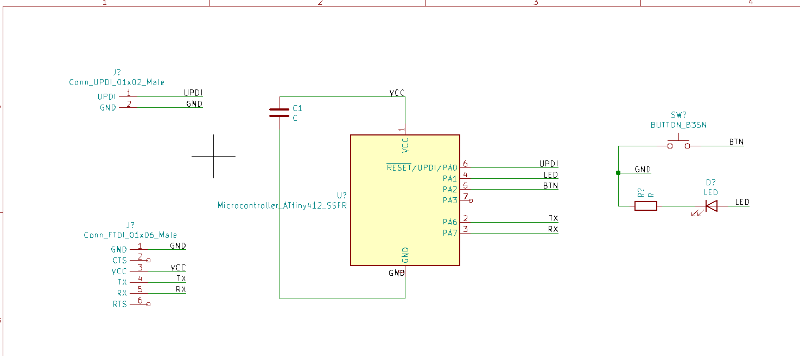
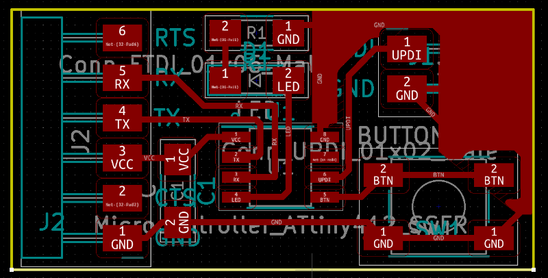
Here I connected the button to the BTN pin (I chose that name, feel free to use whatever you want) and the LED in series with a resistor to the LED pin.
With the small circuit wired, I labelled the pins on the microcontroller to make it very easy to read and avoid the messy pile of wires that it could have become.
3. Annotate components indices
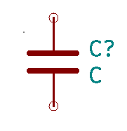
The components being added, you need to annotate them, to differentiate them. Directly after being imported, the components have a “?” next to them. That means they lack an annotation.
You can annotate them by click them individually or by clicking the annnotate tool.
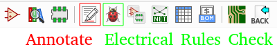
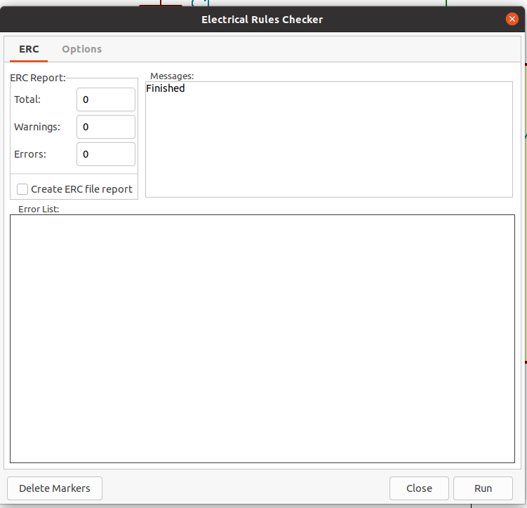
It’s also a good moment to mention the “ladybug” tool. When clicking the ladybug, Eeschema will identify the issues with you circuit.
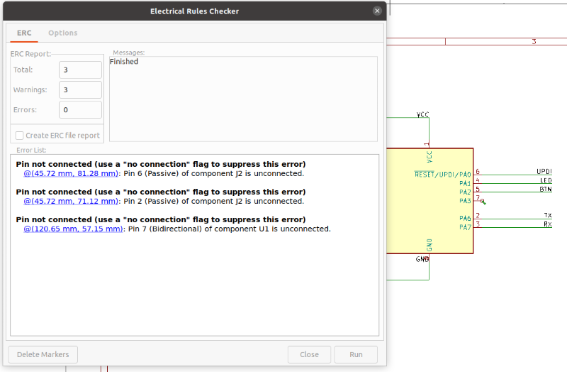
Doing it here gave me the message that I have unconnected pins. That is because I need to have all wires connection status clear. If you don’t want to have them connected, you have to click define them as not connected.
4. Close not connected pins and add power source
To define them as not connected, click the blue cross in the tools and apply it where appropriate.
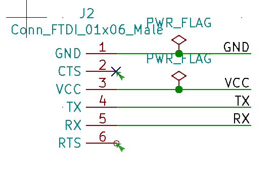
You also need to provide information regarding the position of the power sources, GND and VCC using a PWR_FLAG that can be found in the components list.
Once that is done, you should get to something like this.
And the electrical rules check should not give you any errors.
5. Assign footprints
This is done already done for the fab library components but not others for which you have to do it manually.
You will need to define the footprint of the components that are not in the fab library. But what does that mean ?
Well, for one single type of element in the circuit, you could have different footprints because the electrical circuit in an abstraction of the real one. To select the footprint, right click the component, click Properties > Edit Footprint.
Then you have to choose it in the list.
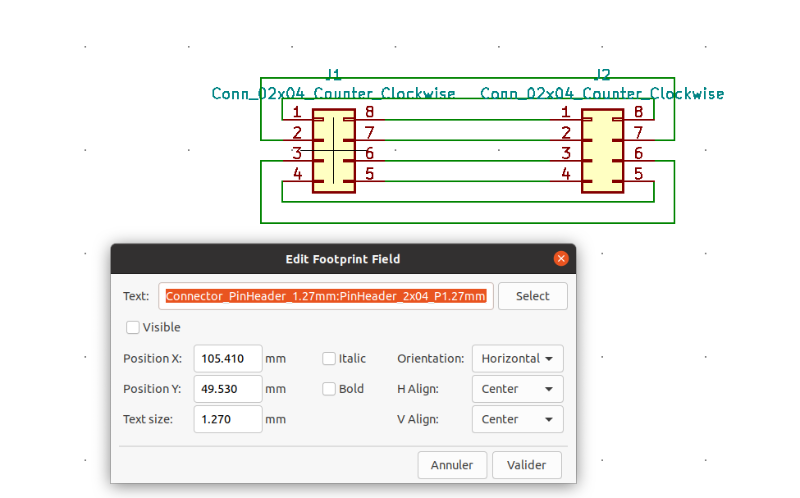
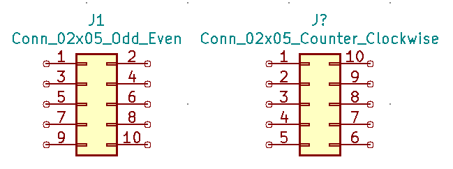
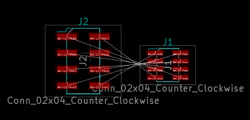
Different things are important to pay attention to: * Select the right spacing, for some components, especially connectors (headers or sockets) you will have to choose between 1.27mm and 2.54mm spacing.
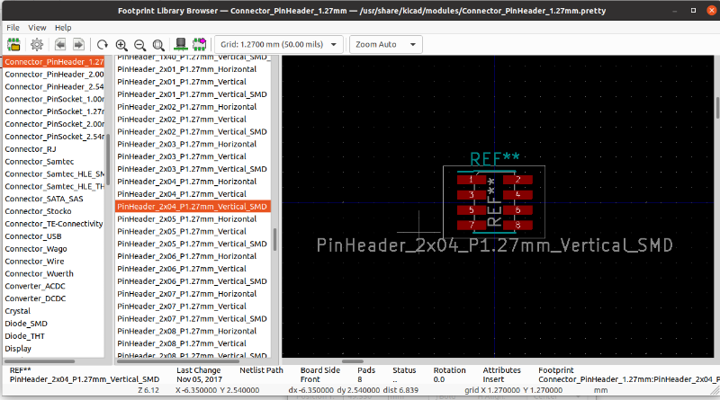
- Select the right pin ordering: Actually, you should pay attention to this when importing the component symbol but it makes sense to explain it here.
When you import a component, especially a connector, you will have the choice between different pin ordering. You should choose the one for which there is an available matching footprint, otherwise, you circuit will not look like the design you planned and it will be very hard to route as such.
When selecting the footprint, you see the numbering of the pins and you can make sur it matches the symbol you are using. Also, when selecting the footprint, in the footprint library, you can see a CAD version of the footprint

This is especially useful to visually check that you have the right component.
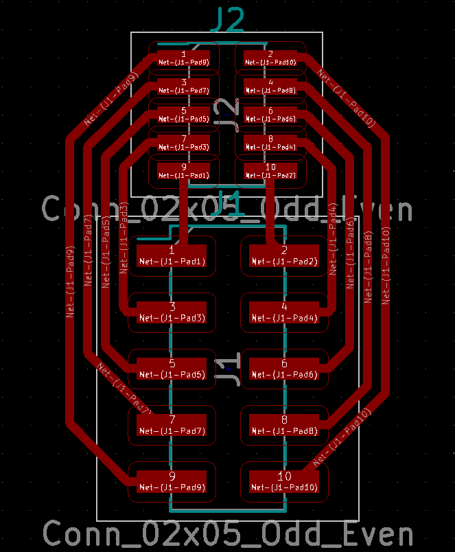
6. Create the PCB Net list
With the circuit complete, you can export a PCB Net list using the NET button.

7. Create the PCBNew Layout
The circuit is finished. You can move to the PCB routing.
To import your circuits, there are two ways: * One is to import it from the schematics * The other is to import it from the NetList you just created.
Be sure to update the circuit when you modify your schematics.
Also, it will not work if you have not assigned footprints to your components.
Once that is done, the first step is to edit the characteristics of your CNC. That is the minimum trace width and minimum clearance.
After that, you can start routing your PCB. Routing means placing a band of copper to make a connection.
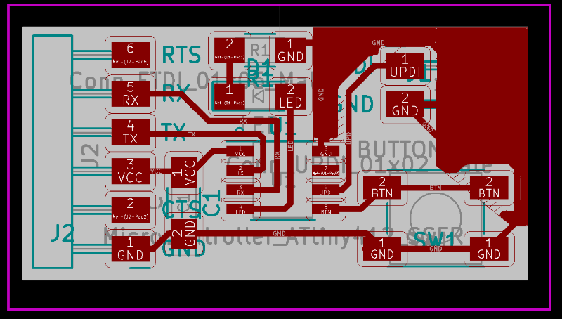
You may well start with something that looks messy
And end up with something very clean.
The important thing is really to set up first the CNC parameters, otherwise you will build route that cannot be milled by your machine.
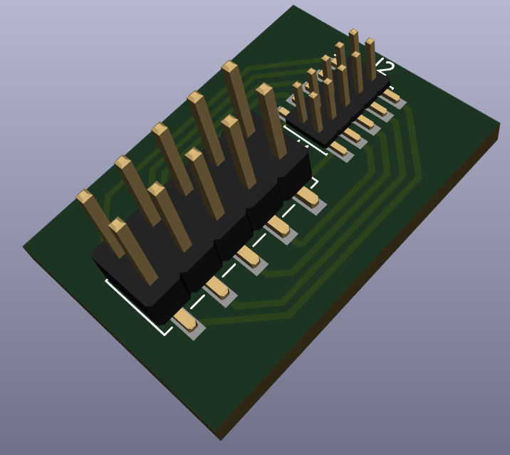
When routing the PCB, you have some freedom in the placement of the components but remember that some need to go out of the boards, such as the RA sockets (RA stands for Right Angle) or RA headers.
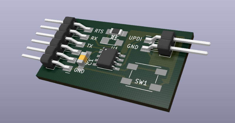
You can see your circuit in the 3D viewer by clicking View > View in 3D.
When routing, there are some rules to follow: theoretically when components are on the same copper trace, the order is irrelevant. However, it is better to put the capacitor first because it acts as a filter for the variation in power. For it to be most effective, it’s better to but it before the microcontroller.
A good practice then is to keep the ground for the latest connection to be made as it will be connected to most elements, it will go everywhere.
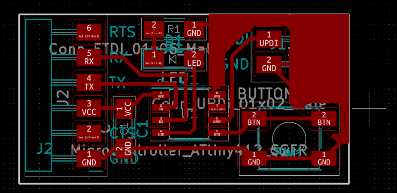
Routing can be a bit tedious in some cases but you’ll manage it. Once you are done you should get to something like this.
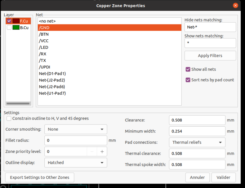
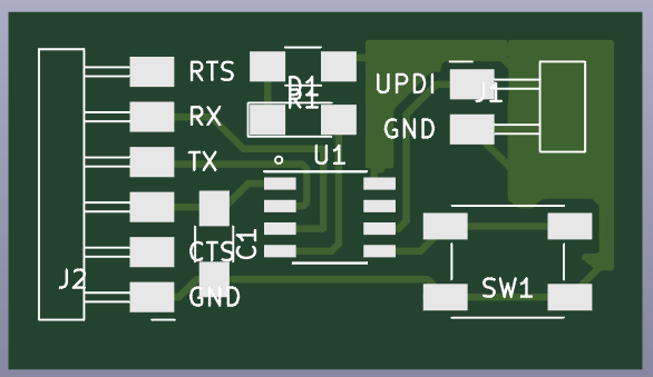
One thing to “simplify” the design or to create a ground plan is to use the fill area tool. This will cover the whole area with copper except the margins around your existing traces and component footprints.
You can do that using the following two tools. With the second one, you can limit the automatic filling in an area that you define.

To fill copper, you have to select the area you want to cover but also define what net, or what pin you want it connected to. In this case, we want ground aka GND.
After that we can add cut lines on the sides, so we change the layer we are using :

We add graphic lines, available in the left tool bar.
The Edge cuts layer appears in yellow so we get this.
It is also a good idea to add margins, especially if you plan on using mods to create the tool path. For mods also, you will need a solid background for the edge cut that you can add in Dwg_User and the “Graphic polygon” tool.
Once that is done, you get to this result
If we want to look at it, before printing we can click View > View in 3D.
If like me the components are missing, it means that you did not link the fab library models properly so go back to Chris’s video or go to Preferences > Configure path and link the good folder.
Once it’s properly linked you should see most components even if some 3D are missing.
We have a Bantam Tools CNC and thus we can use Gerber files which are more convenients than gcode imho.
To export Gerber files, go to File > Plot, select the layers you want and deselect the non-necessary items in the General options. Especially the Border and title because otherwise, it will make the CNC software bug.
Producing the board
I milled the board and started soldering.
As I was soldering, I was continuously checking some connections to make sure it was working.
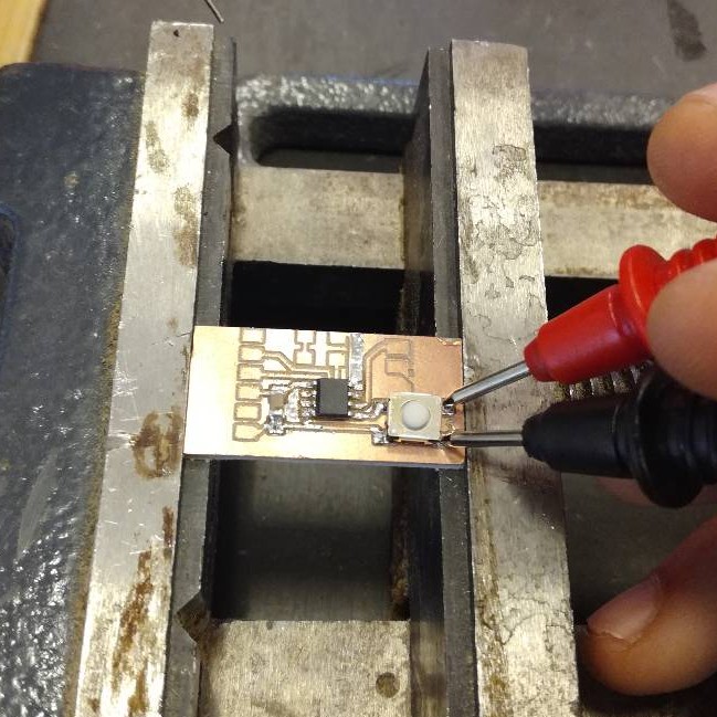
One thing, I did not know before is that the multimeter provides enough voltage to light up the LED and a low enough current not to burn it, which it incredibly useful to avoid mistakes as diods (thus LED - Light Emitting Diods) must be placed is a specific direction.
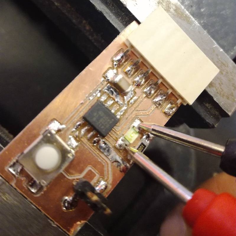
We wanted to make another board with NeoPixel but the design we had made was bigger than the copper board…
Quentin also showed us the acid tin solution that he had bought to tin his circuits which was pretty cool.
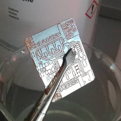
As I wanted to test my CNC, I started by producing a martyr board (spoil board) and doing that I tried Easel to control the CNC that we were using.
Loading a program
To program my AtTiny412 circuit, I used Quentin’s UPDI programmer, a SAMD11C based serial converter, taking Serial USB and writing it on the Serial pins.
Quentin’s programmer has an included connector to select the power to provide (5V or 3.3V) and a possibility to short the TX and RX pins through a 4.7k resistor which makes it a UPDI programmer.
I did just that and selected in the Arduino IDE UPDI and as a programmer Serial port and 4.7k (pyupdi style)
For more on programming, check the embedded programming week
Files
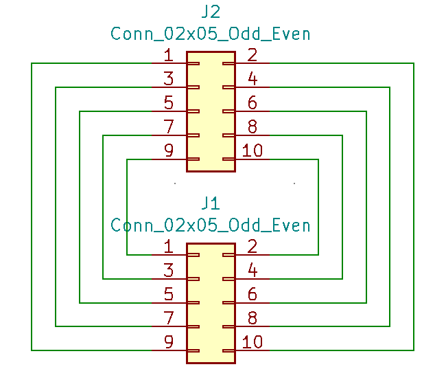
- KiCAD project for 1.27 to 2.54 mm connector
- AT Tiny 412 with a Led and a button
- Code to Blink the Led on the AtTiny412 Board