'Cutting your fingernails on the day you are travelling is a calculated risk.'
African Proverbs
Week 6 Assignment
This week, we are charged to do a group assignment, and two individual assignments. These are given below:
Group Assignment
You can view the Group Assignment on this Link.
Individual Assignment
Software
I will attempt to execute this task with more than one software. So I will use the following softwares to design or redesign the electronic component:
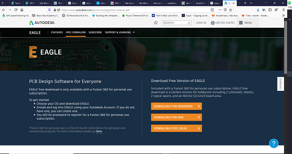
EAGLE which stands for Easily Applicable Graphical Layout Editor, is a scriptable electronic design automation (EDA) application with schematic capture, printed circuit board (PCB) layout, auto-router and computer-aided manufacturing (CAM) features. The software contains a schematic editor, for designing circuit diagrams. Schematics are stored in files with .SCH extension, parts are defined in device libraries with .LBR extension. Parts can be placed on many sheets and connected together through ports. More information can be found HERE.
To download the software, simply visit this LINK.
After download is complete, and the software has been installed, then you can sign in into an account. For those already signed up for Fusion 360, you can simply sign in with your Fusion 360 account. However, if this is your first time using any Autodesk product, then you have to create a free account 'Educator'.
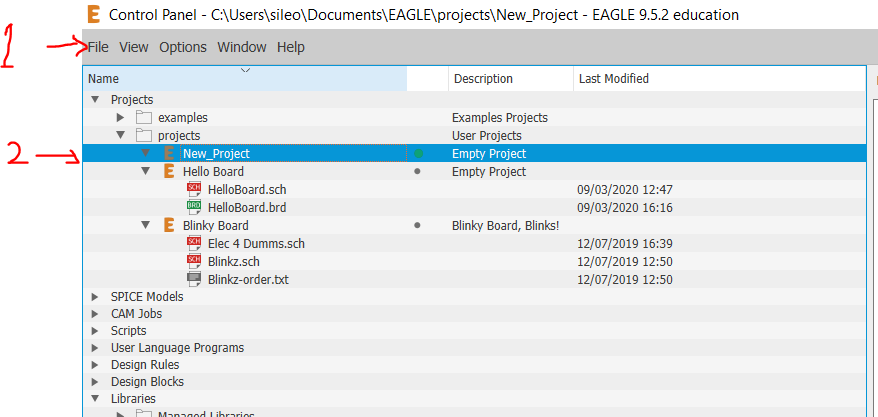
After your account has been set up and signed into, then you can proceed with the creation of your first project by clicking 'file' then 'New Project'. After this, you can enter a unique name for your project, in my case I used 'Hello Board' as depicted in the illustration below. Then go back to File, then select 'Schematic'.
Before we proceed, it is worthwhile to provide a brief axplanation about what we mean by a schematic.
What is a Schematic?
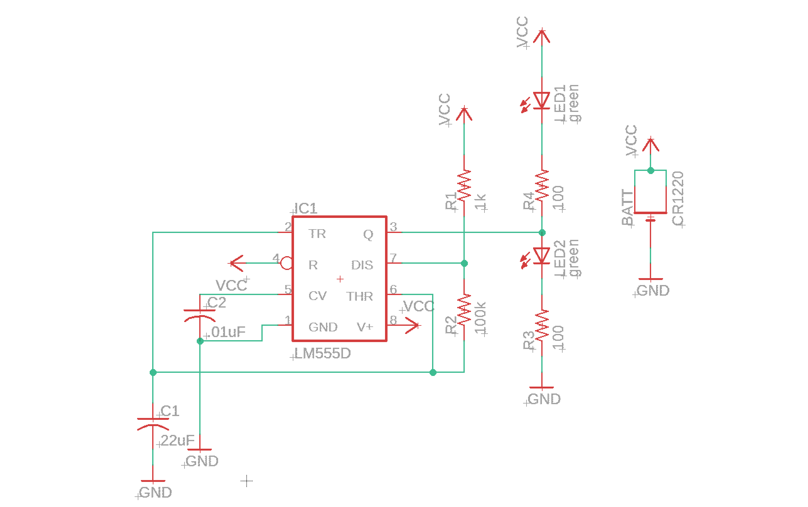
A schematic in electronics is a drawing representing a circuit. It uses symbols to represent real-world electronic components. The most basic symbol is a simple conductor (traces), shown simply as a line. If wires connect in a diagram, they are shown with a dot at the intersection. The illustraion depicted below represent a sample Schematic for an Electronic component that blinks using an LM555D transistor and some other components such as LEDs, Resistors, and a Battery connector:
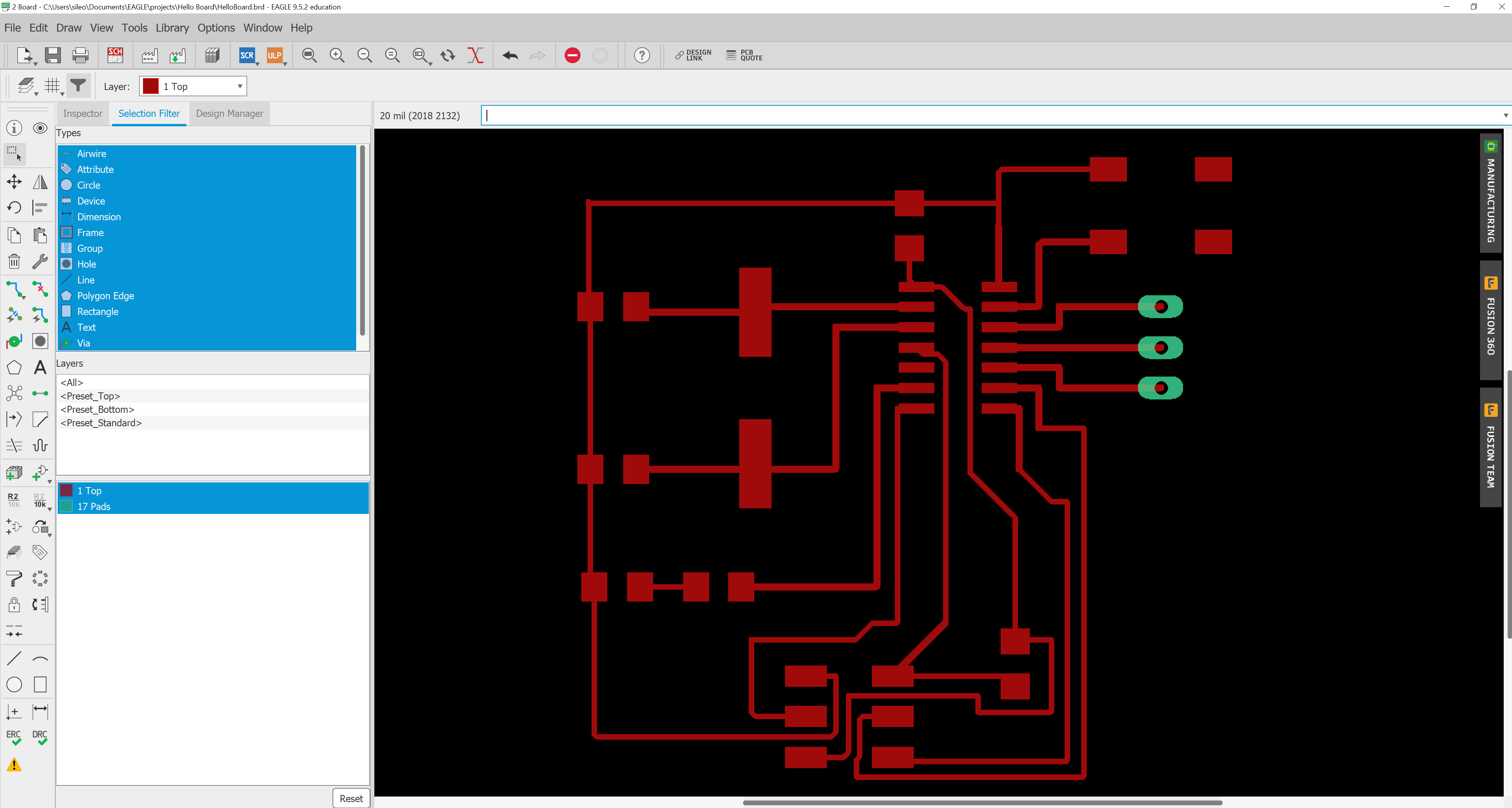
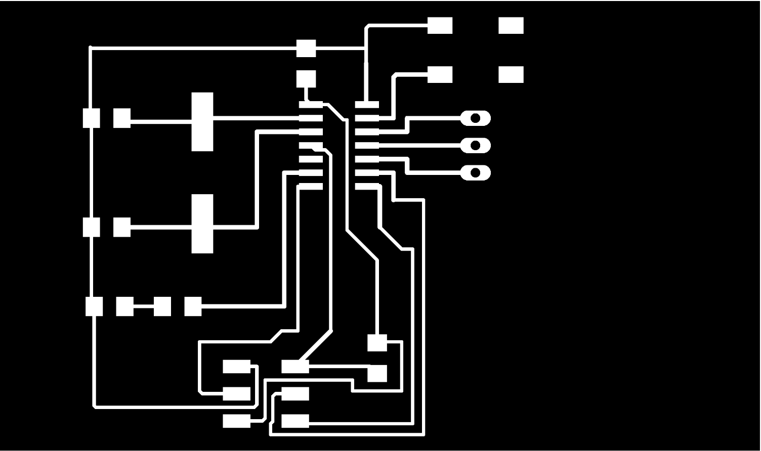
In addition to the schematic layout, there is also a 'Board' layout on the Eagle software. What the board layout shows is how the electrical components and traces will be laid out on the board. It shows you what your electronic circuit board would look like or better still, it gives you an opportunity to determine how the circuit layout should look. This is depicted in the picture below.
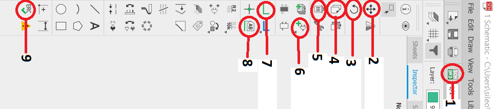
In order to do the assignment, you at least need a basic knowledge of some of the menus on the Eagle software. the illustration below explains some of the most useful buttons.
After this basic introduction, we can now proceed with the assignment. Which is to redesign Echo Hello-World board.
Before we proceed, please be aware that this is not rocket science. So it is advisable that you consult the datasheet of the components to know elicit the vital information about it. This will help you create an ideal electronic circuit that works. If properly studied, you will know the type of components that can be utilized with it, as well as the size and other critical information. So I suggest you check that first before you proceed. For example, search 'ATTINY44 Datasheet'. From this document, you will know the size of resistor that can be used with this microcontroller. The RAM size embedded within it, and so on and so forth.
Library
Just as a physical Library contains millions of knowledgeable books and materials, so does the library in Eagle contains thousands, if not millions, of useful electronic components which can be inserted at will.
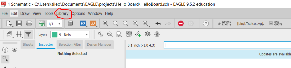
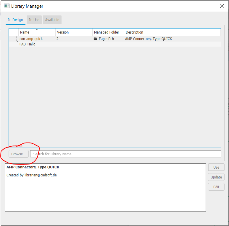
To add a new library (this can be done after opening the schematic), for example, we can use this one by Adafruit, after the download, then click the 'Library' as shown in the picture below, then click 'Open Library Manager' which will show something similar to the second picture below. Then click 'Browse' to select the folder containing the library to be added. Then click 'OK'.
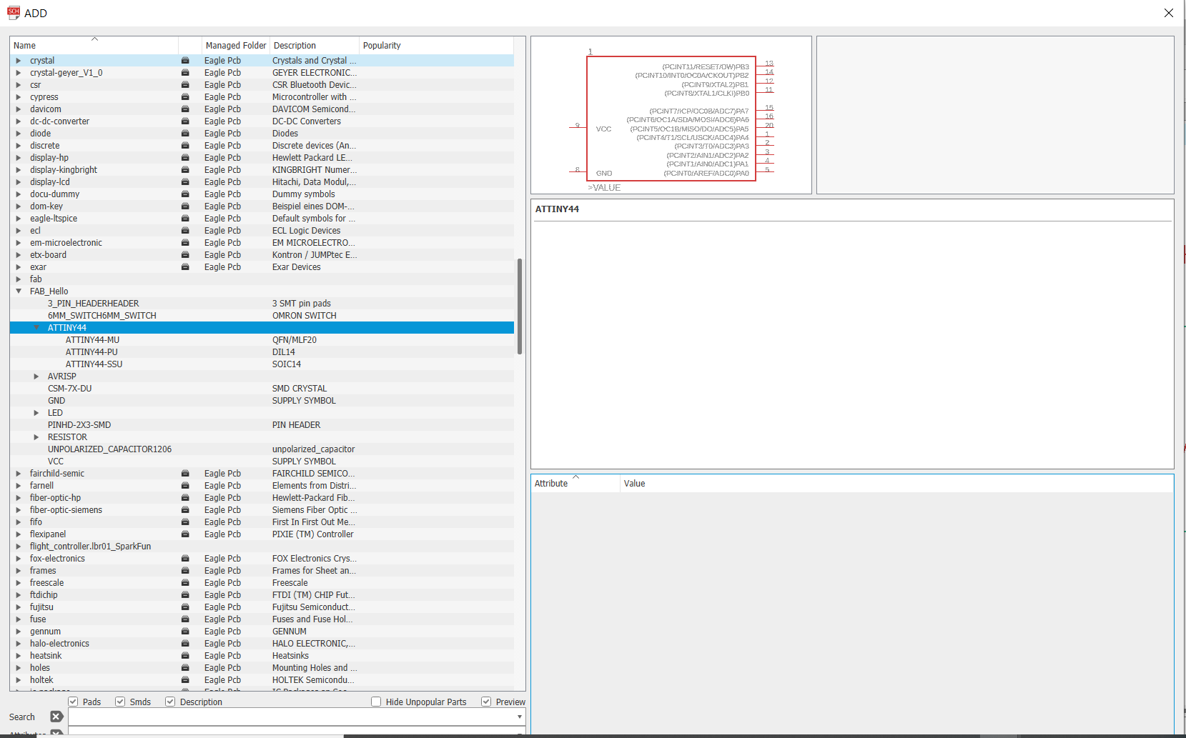
In this case, Daniele already sent us the libraries to add or use for our assignments (FabHello.lbr, fab.lbr, etc). I am sorry for those who do not have a good Fab Instructor! So after adding these libraries, I proceeded with adding the components needed for the assignment on the schema.
So instead of using the 'Net' I decided to go green and be clean. I used Label instead. Below, you will find the final schematic layout of the assignment.
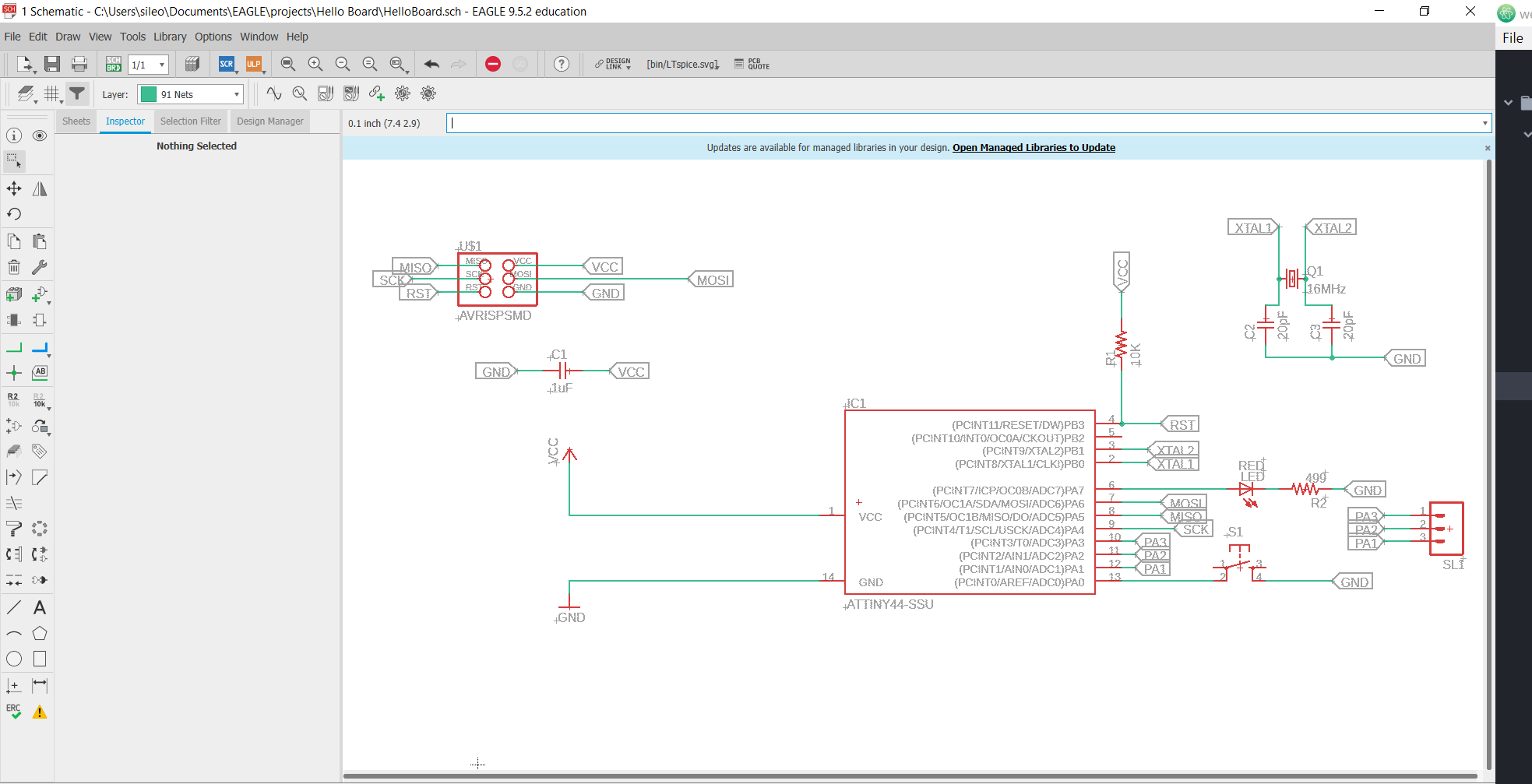
After this, we use the SCH/BRD button to toggle between the schematic layout to the Board layout. The first thing you would see after changing from schematic to board layout is that the components are all dumped on the left-bottom part of the screen. There is no cause for alarm, all you have to do is to move them right in the middle of the work area. Then you can start rearranging the components in a manner that makes it easy to trace the circuit.
Rule of Thumb! As Daniele Ingrassia sazs, consider the microcontroller (in this case ATTINY44) as the centre of the universe when rearranging the components on the board. I reckon and suggest this as well, because as you will soon see, it takes a virtue to untangle and rightly rearrange the components properly.
Once you are done with the rearrangement and tracing, then you need to do one final check before producing your circuit board. You need to do the DRC - Design Rule Check. This is similar to the ERC that was done at the end of the schematic design layout. This also verifies that the board layout will meet the basic requirements to be considered during the fabrication phase (that is, milling).
Board fabrication
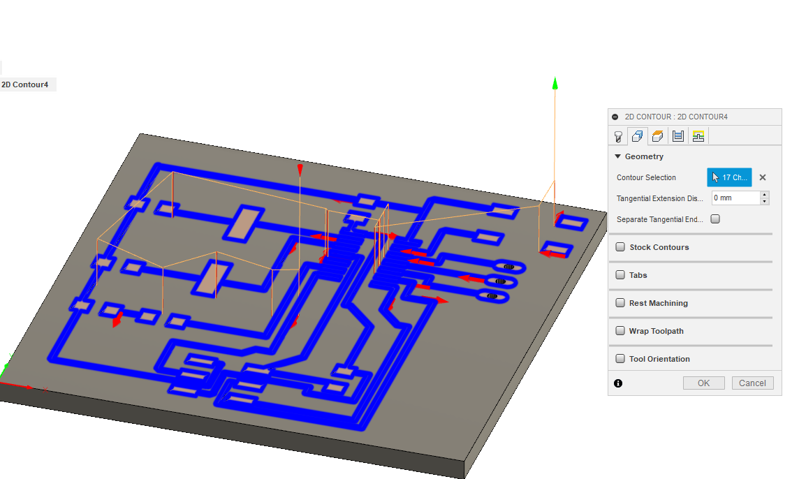
After concluding the design on Eagle and saved as PNG file. The next step I took was to convert the PNG file to DXF, and import it to Fusion. If you are wondering why I did this, kindly revisit my assignment on Electronic Production. That been said, I used the very same method used to mill the FabISP board. This will be represented in the pictures below.
First, I inserted it in Fusion360 as DXF. To do this, go to 'Insert' --> 'Insert DXF'
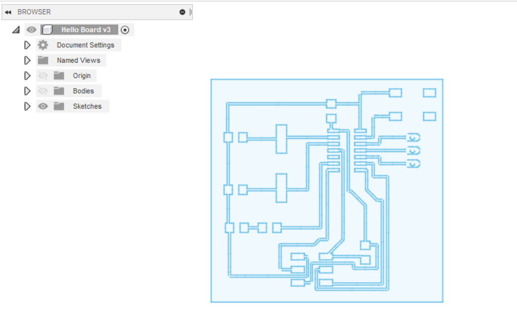
After this, I simply extruded all the sketch to the height of my PCB board. Then I changed the appearance of the traces to copper so it can be visible and pretty.
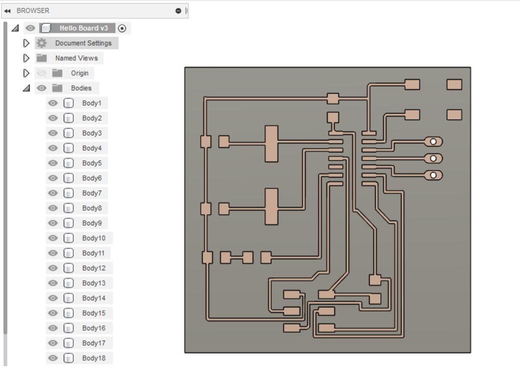
One thing I must advise here is that the job will be extremely bigger than the required size. So what you need to do is to check the dimension of the design in Eagle, then scale the job down to the size on Eagle. To do this on Fusion360, go to:
'Modify' --> 'Scale' --> 'Non Uniform'
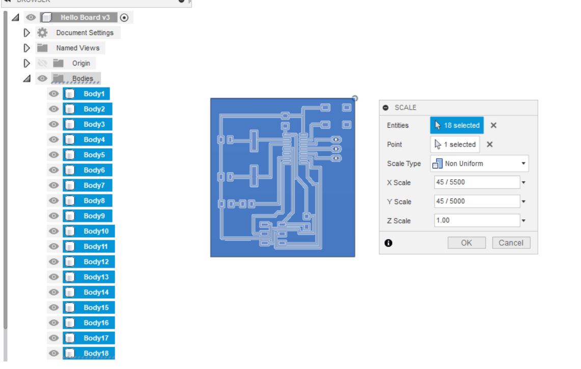
For the scale, as can be seen on the picture above, I divided the required size by the extruded size.
Scale = Required Size / Extruded Size
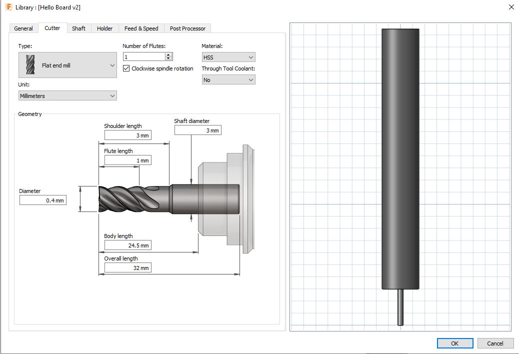
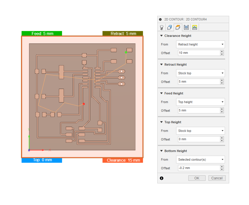
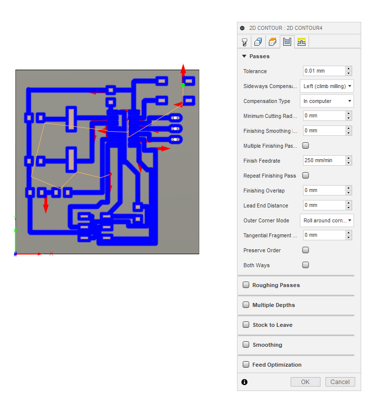
After this, I just set prepared it for fabrication by setting up the tool and other gymnastics.
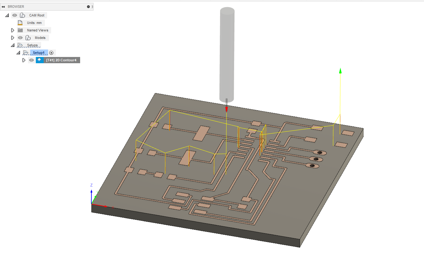
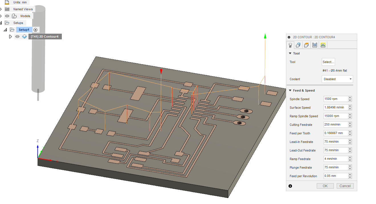
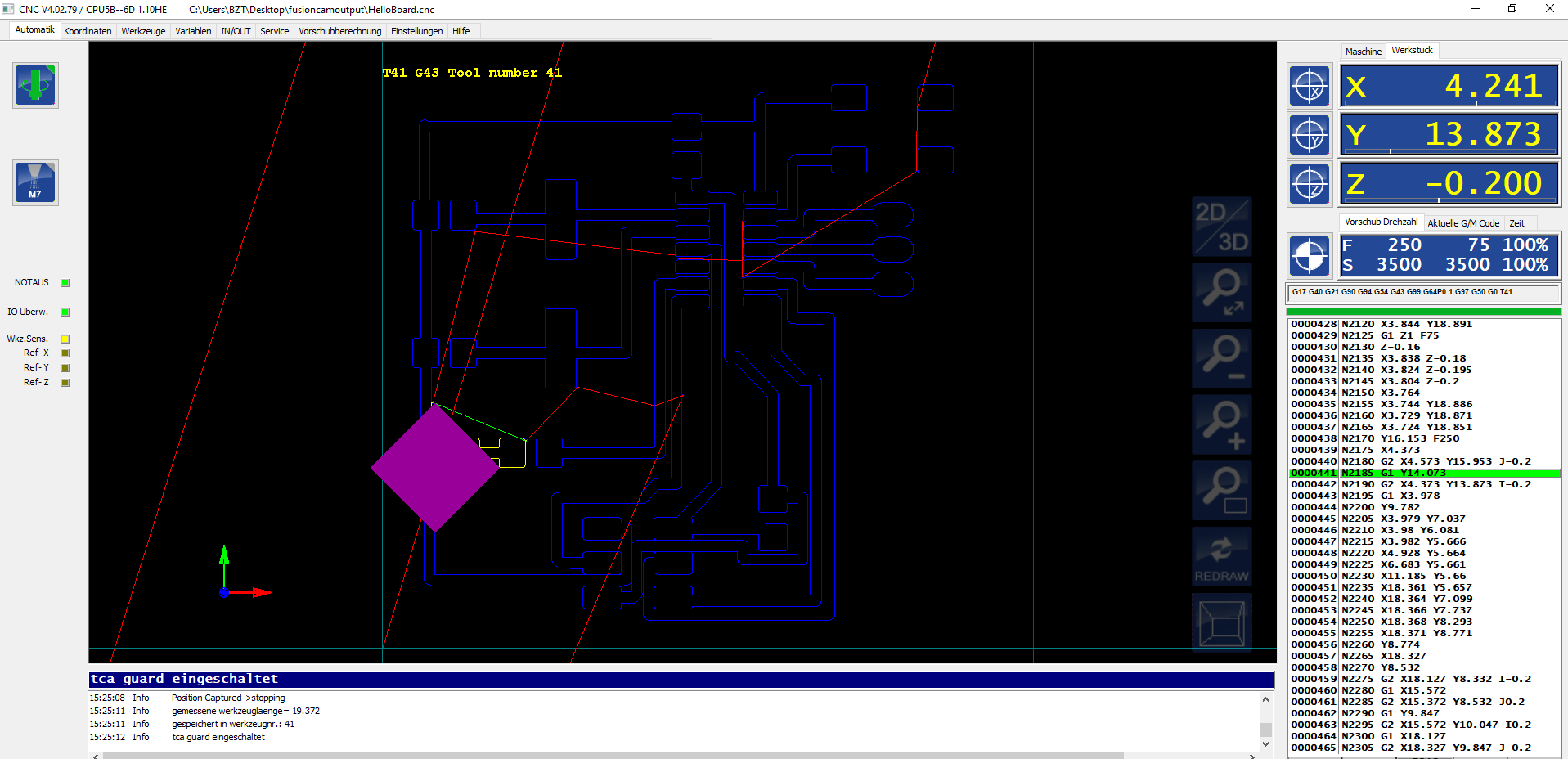
After all these, I did a simulation to know how the PCB will be milled, and to know whether there are any collisions or things I should be concerned about.
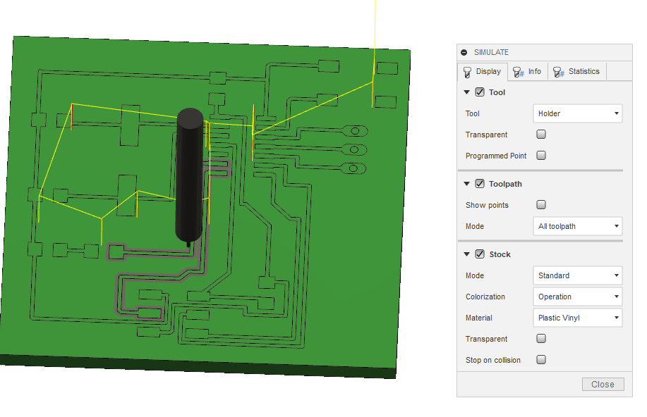
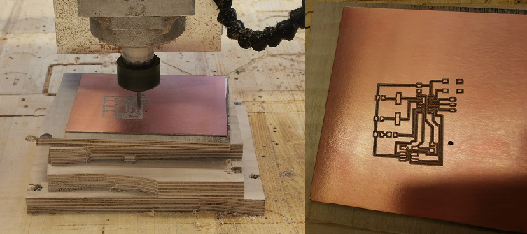
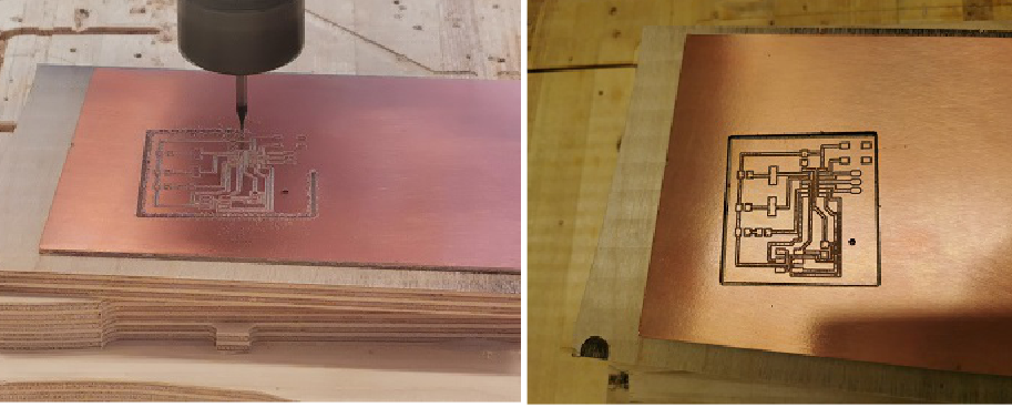
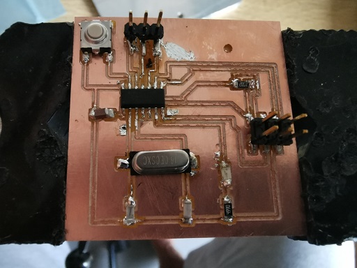
After this, I simply did a post process to generate the G-Code for the job. Then I prepared the machine and started milling. You will find the pictures of the job below.
Stuffing
After this, I stuffed the board. Below are the components used for the board.
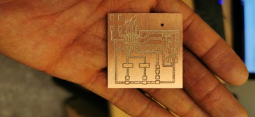
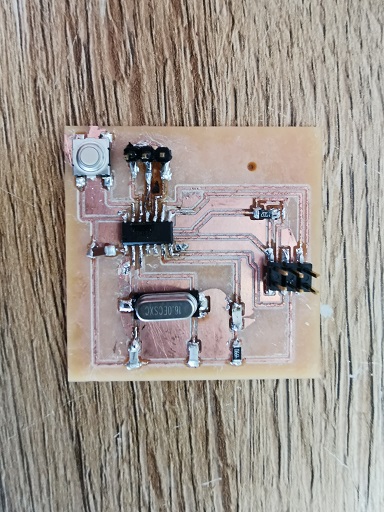
After this, I learnt a lot from the errors I had when doing the Electronic Production assignment. I then stripped off the copper layer of the board so as to prevent causing other bridging with the board.
After this, I will proceed to programming the board.
Programming and Testing
To program the board, you have to connect the FABISP to the Hello Board. NOTE: Ensure that you connect the board to its exact connector on the Hello Board. That is, VCC --> VCC, MOSI --> MOSI, GND --> GND, etc. In case you make a mistake, just try to fix the connection as soon as possible.
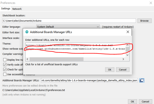
After this, then you have to open the Arduino IDE. Then go to 'File' --> 'Preferences'. In the 'Additional Boards Manager URLs' box, enter theis link below:
https://raw.githubusercontent.com/damellis/attiny/ide-1.6.x-boards-manager/package_damellis_attiny_index.json
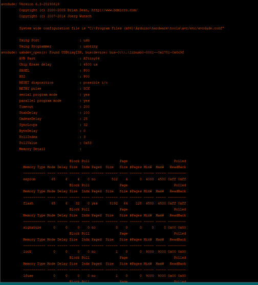
To finish the upload, you can follow this Link. However, after selecting all the necessary parameters of the board, I clicked 'Burn Bootloader. After which I kept getting this error message below.
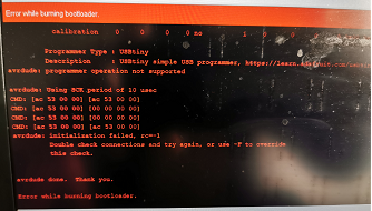
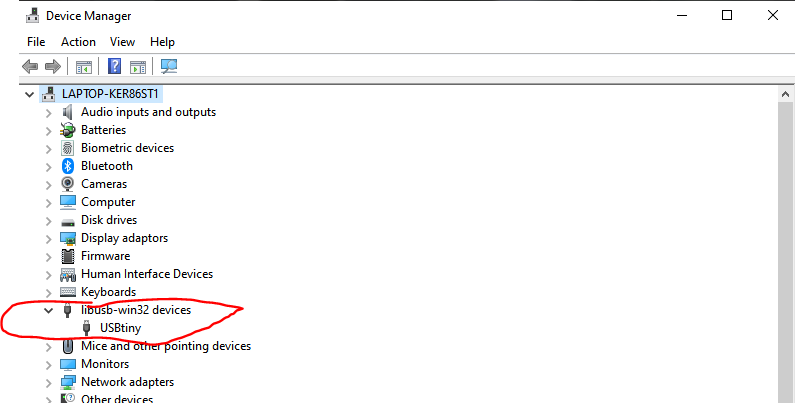
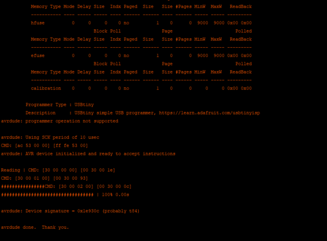
Then I checked the Device Manager to see whether it was detecting the board. Which I confirmed to be true, but not the exact name. The name of the board programmed in Assignment 4 is USBTinySPI. However, the name displayed on the device manager shows 'USBTiny'.
In addition to this errors, while trying to be clever. I used super glue to fix the jumper cables together. However, while trying to pull it from the Hello board, I destroyed the soldering of the 2x3 pin header. Which makes this the second damaged board and still could not understand what the issue is and where they are coming from (Aaaaaaaaargh!).
So just like the Ghostbusters' song, which says
If there's something strange
In your neighborhood
Who you gonna call?
Ghostbusters!'
Since I was experiencing what seems like a paranormal activity on the assignment, I called my Errorbuster, my Fab Instructor. With his help, I was able to identify and resolve the issue with the board.
The issue we identified was that I was connecting the VCC of the FABISP to the VCC of the Hello Board. So the two options I had was to either disconnect the VCC and power it through an Arduino board, or 2. Connect the VCC and solder the jumper part of the FABISP board.
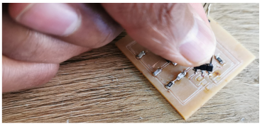
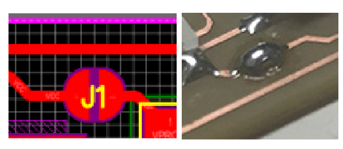
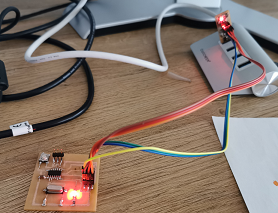
I opted for the second option, and resoldered the jumper of the FABISP board. See picture below
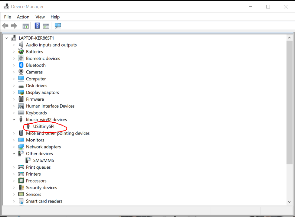
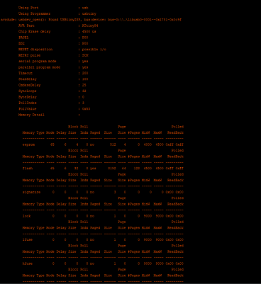
After this, I checked the device manager, and I noticed the name had changed to USBTinySPI (unfortunately, I failed to take a picture of this. I thought I would be able to find it afterwards. Sorry!). However, it shows something similar to the one below.
Which shows a sign that everything is eventually going to work out just fine. However, I was a little bit nervous to run the code, but I did and everything worked.
Test
After this, I simply uploaded the 'Blink' example on Arduino to check if the board is fine. However, do not forget to change the Pin number on the Arduino sketch to the port number used on your board. Below you will find my code.
/*// the setup function runs once when you press reset or power the board
        void setup() {
          // initialize digital pin LED_BUILTIN as an output.
          pinMode(7, OUTPUT); //I changed this to 7, since I used PA7 on ATTINY84 microcontroller
        }

        // the loop function runs over and over again forever
        void loop() {
          digitalWrite(7, HIGH);   // turn the LED on (HIGH is the voltage level)
          delay(1000);                       // wait for a second
          digitalWrite(7, LOW);    // turn the LED off by making the voltage LOW
          delay(1000);                       // wait for a second
        }
Then I compiled the sketch, and VOILA!
Click on this LINK to download my new design of the Hello World assignment.
Lessons Learnt
The vital lesson I learnt in this assignment is how to measure the distance between 'Now' and 'Then', also the distance between 'Before' and 'After'.
Do not be fooled by all these quick fix commercials.
The distance between Now and Then, or Before and After is a quotient of Patience, Resilience, and Determination.
"Q.E.D."