Week 8. Electronics Production
Group Assignment
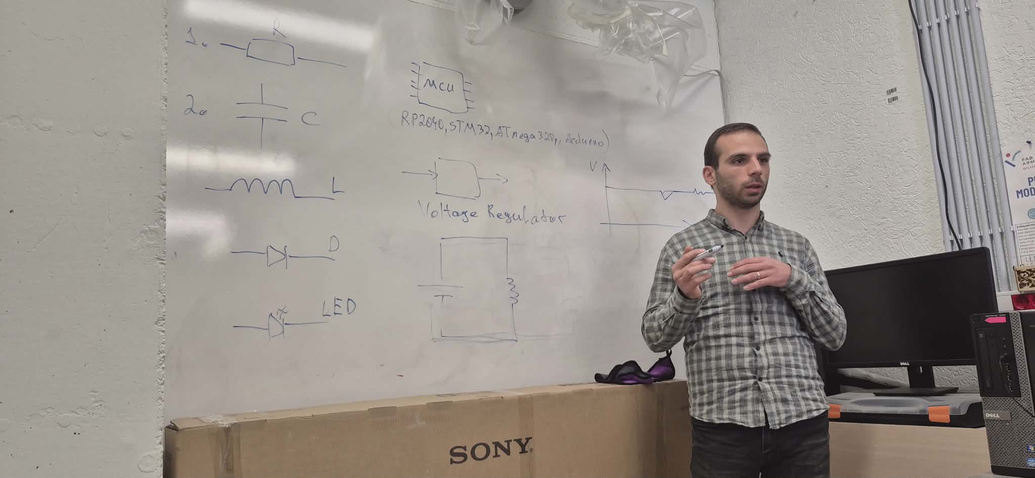
Electronic Components
This week, our instructor Onik Babajanyan introduced the main electronic components and explained their roles in electronic circuits. These included resistors, capacitors, LEDs, diodes, MOSFETs, voltage regulators, and transistors.
Inductor
An inductor is an electronic component that stores energy in the form of a magnetic field. It is usually made from a coil of wire and is commonly used in filters, power supplies, and various electronic circuits.
Diode
A diode is a semiconductor component that allows current to flow in only one direction. It is widely used for rectification and for protecting circuits from reverse polarity.
MOSFET
A MOSFET is a type of transistor that acts as an electronic switch or amplifier. It is voltage-controlled and allows switching large currents using a small control signal.
LDO (Low Dropout Regulator)
An LDO is a type of voltage regulator that provides a stable output voltage even when the input voltage is only slightly higher than the output voltage. It is commonly used to power microcontrollers and other sensitive electronics.
Voltage Regulator
A voltage regulator is a component or circuit that maintains a constant output voltage regardless of variations in input voltage or load conditions. It is essential for the reliable operation of electronic systems.
During the group assignment, I worked with my teammates Gevorg, Mariam, and Hrach.
Our main goal was to study and define the design rules used for PCB milling in our lab.
We:
- studied the limits of trace widths and clearances,
- tested different tools and parameters,
- determined the acceptable ranges for reliable production.
Milling Process
To fabricate a test PCB sample, we followed these steps:
- Configured VPanel to control the CNC machine,
- Fixed the PCB board into an MDF base,
- Set the zero positions for the X, Y, and Z axes,
- Generated G-code and verified the toolpaths.
During the testing process, we used two different milling tools:
- a 1/64 flat end mill for precise PCB traces,
- a 30° V-bit with a 0.1 mm tip diameter for comparison tests.
The goal of this experiment was to compare the effect of different tools on PCB milling quality and determine which one is more suitable for precise work.
Tool Comparison
The tests were performed using a 1/64 flat end mill and a 30° V-bit.
During the testing process, we used two different milling tools:
- a 1/64 flat end mill for precise PCB traces,
- a 30° V-bit with a 0.1 mm tip diameter for comparison tests.
The goal of this experiment was to compare the effect of different tools on PCB milling quality and determine which one is more suitable for precise work.
Tool Comparison
The tests were performed using a 1/64 flat end mill and a 30° V-bit.
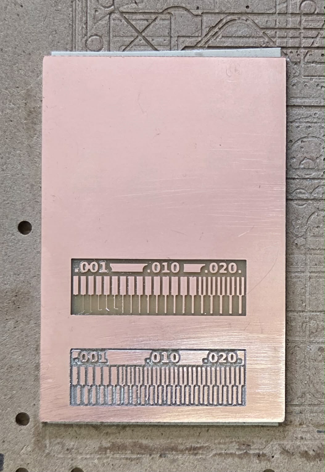
During the experiments, we used the Mods software to generate G-code from design files, which allowed us to precisely control the milling process and adapt the toolpaths to our machine parameters.
Additionally, as part of the assignment, we sent a PCB design to an external board house to study the external manufacturing process and compare it with our in-house workflow.
This group work provided us with practical experience in PCB design and milling, and helped us better understand manufacturing constraints and their impact on the final result.
PCB Production Process
The goal of this group assignment was to document the complete process of sending a PCB design to a boardhouse, from preparing the manufacturing files to placing the final order. The assignment was carried out together with Mariam, Hrach, and Gevorg, with the support of Rudolf Igityan. To demonstrate the process, we used the PCB designed by Mariam and prepared it for manufacturing.
Since the PCB had already been designed in KiCad during the previous week, our focus in this stage was on generating the files required for production. First, we reviewed the PCB layout and verified that all traces, connections, vias, and the board outline (Edge Cuts) were correctly defined.
Next, in Fabrication Outputs → Gerbers, we selected the required layers and generated the Gerber files. From the same section, we also generated the drill files containing the information about all holes on the PCB.
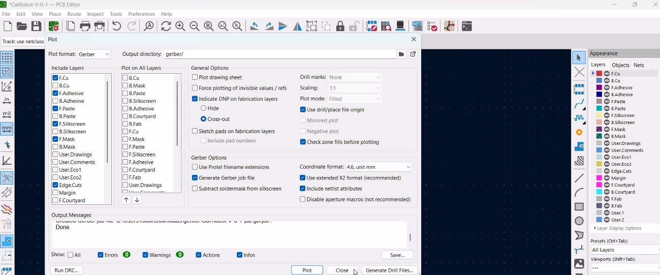
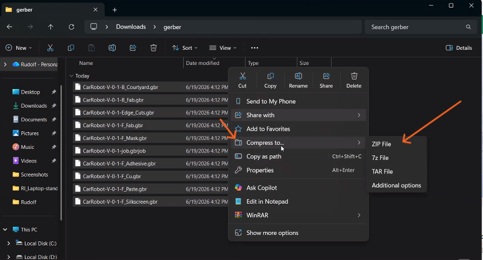
Afterward, all manufacturing files were collected into a single ZIP archive and prepared for upload to the boardhouse.
The next step was to visit the PCB manufacturer’s website and upload the generated files.

The system automatically analyzed the files and displayed a preview of the board, allowing us to verify that all layers, holes, and dimensions had been interpreted correctly.
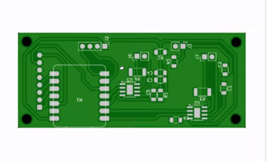
We then selected the required manufacturing parameters, including the PCB material, thickness, color, and other production settings.
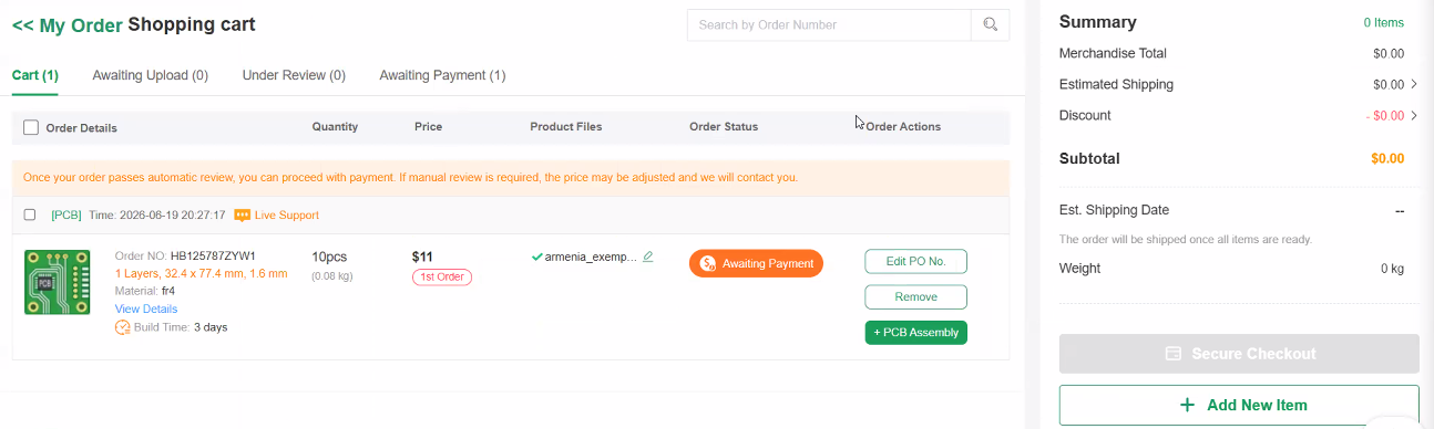
Finally, we completed all the main steps of the order setup and selected the shipping option. At this stage, only the payment step remained, requiring the addition of a bank card to finalize and confirm the order.
More detailed information about this process can be found on the group page.
Individual assignment
In my individual task, I decided to mill the board that I designed during Electronics Design week. The goal was to create a functional system combining sensors and output devices to interact with the environment.
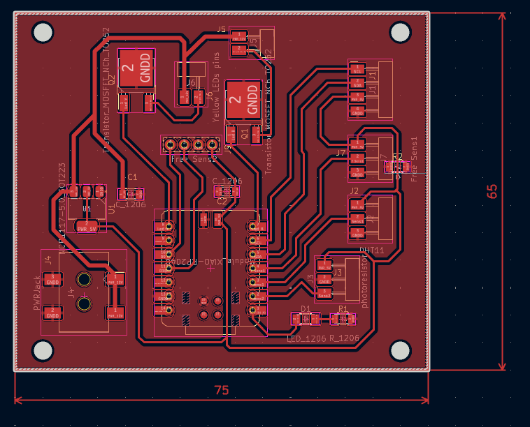
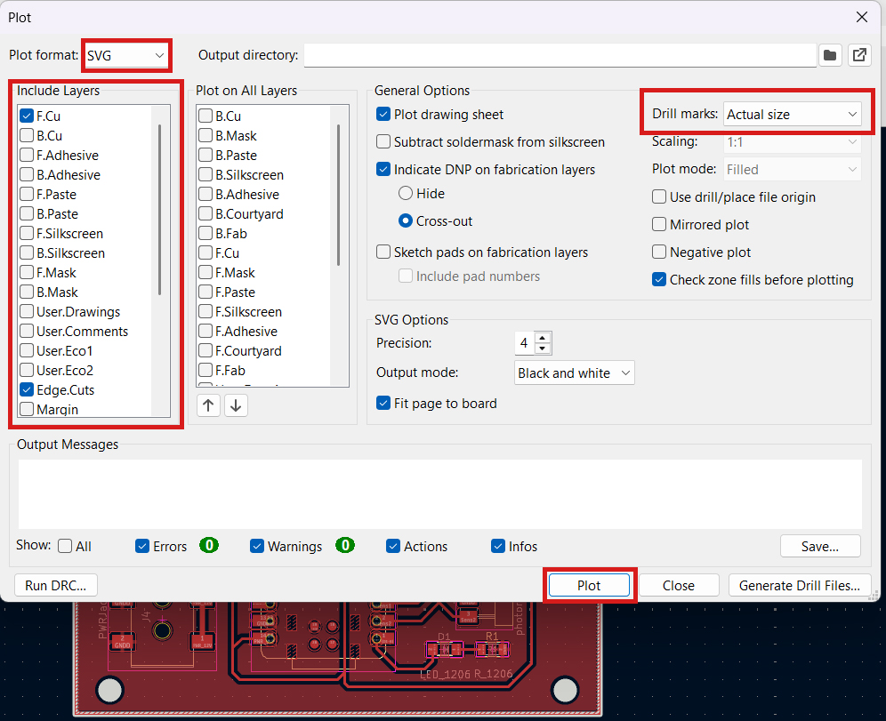
After preparing the file for export, I navigated to File → Fabrication Outputs → Gerbers (.gbr). In the opened window, I changed the plot format from Gerber to SVG to match the required output format for further processing.
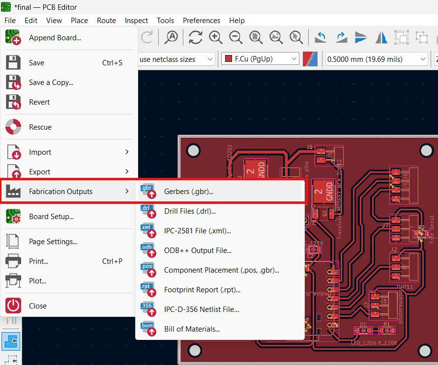
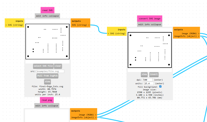
I then exported the PCB design in SVG format, as it is vector-based and ensures high precision. At this stage, I selected only the necessary layers — F.Cu and Edge.Cuts — since the board is single-sided and does not require the use of the *B.Cu layer. This helps avoid unnecessary data and reduces the risk of errors during the fabrication process.
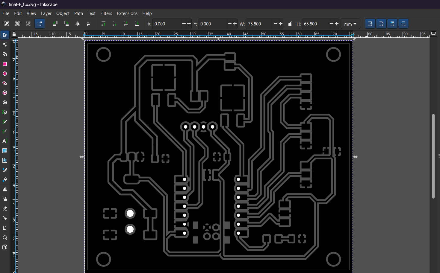
Before that, I opened the exported SVG file in Inkscape to verify that the dimensions of the PCB had not changed during the export process.
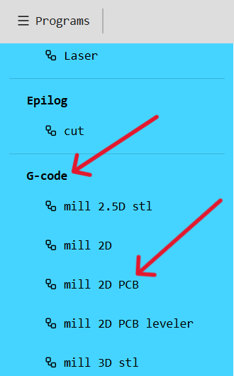
Next, I proceeded to generate the G-code. I accessed MODS Project through the browser and, from the available options, selected Mill 2D PCB in the G-code section. This step allowed me to prepare the toolpaths and generate the final file required for the milling process.
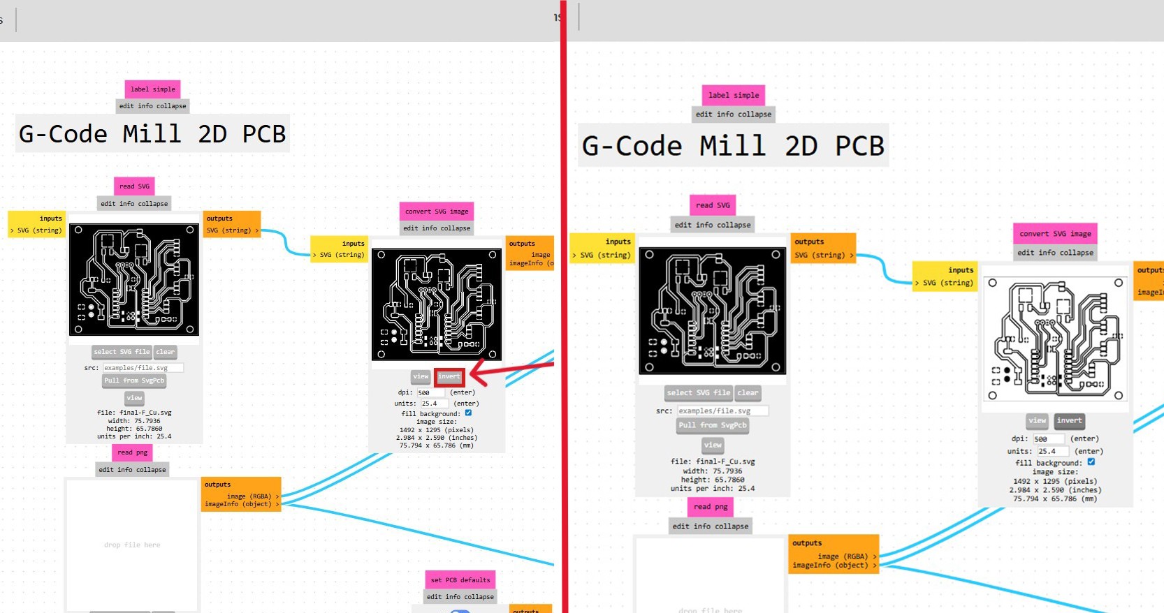
At this stage, I applied the invert operation, since in the milling process the black areas are interpreted as material to be removed. This ensures that the copper traces are preserved while the surrounding material is milled away.
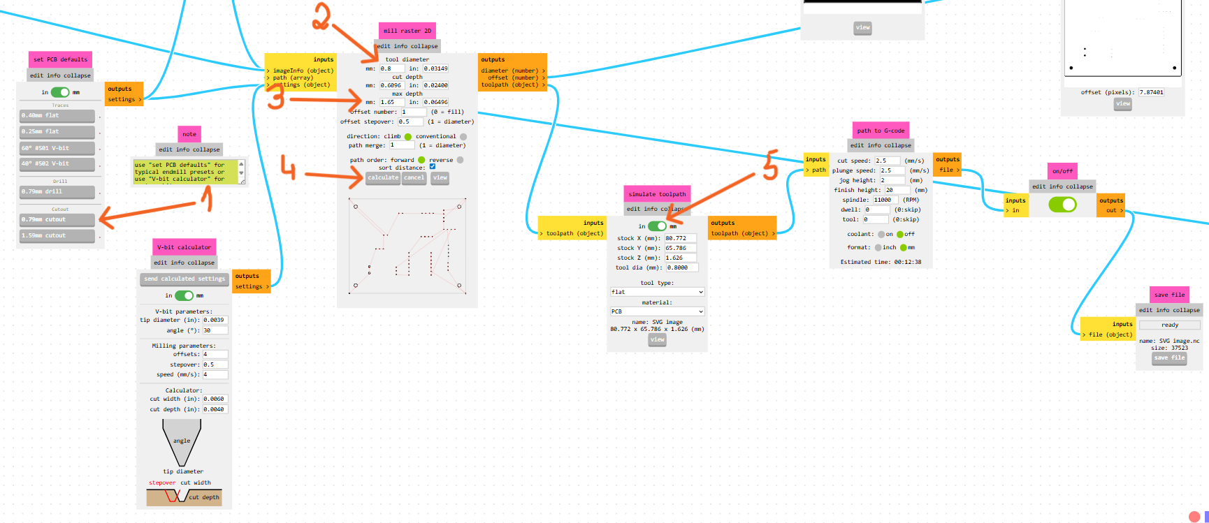
In the next step, I defined the milling parameters, including the tool diameter and cutting depth. These values were selected based on the required precision of the traces as well as the capabilities of the machine, ensuring accurate and reliable milling results.
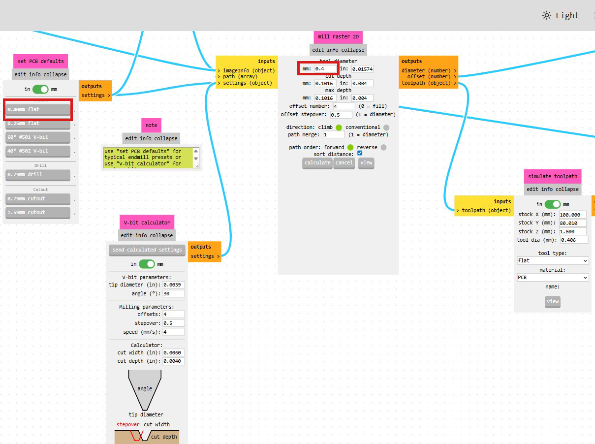
After defining the milling parameters, I first activated the on/off switch (1) to enable the automatic workflow. This means that after pressing calculate, the result would be immediately passed through the modules and prepared for saving.
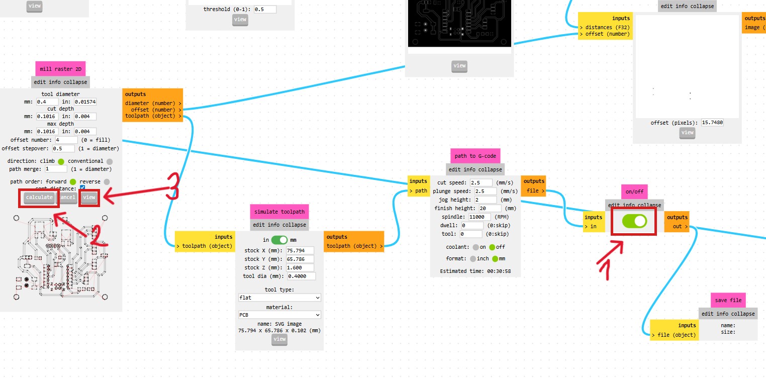
Then, I clicked the calculate button (2), and the program generated the toolpath and automatically forwarded it to the next modules.
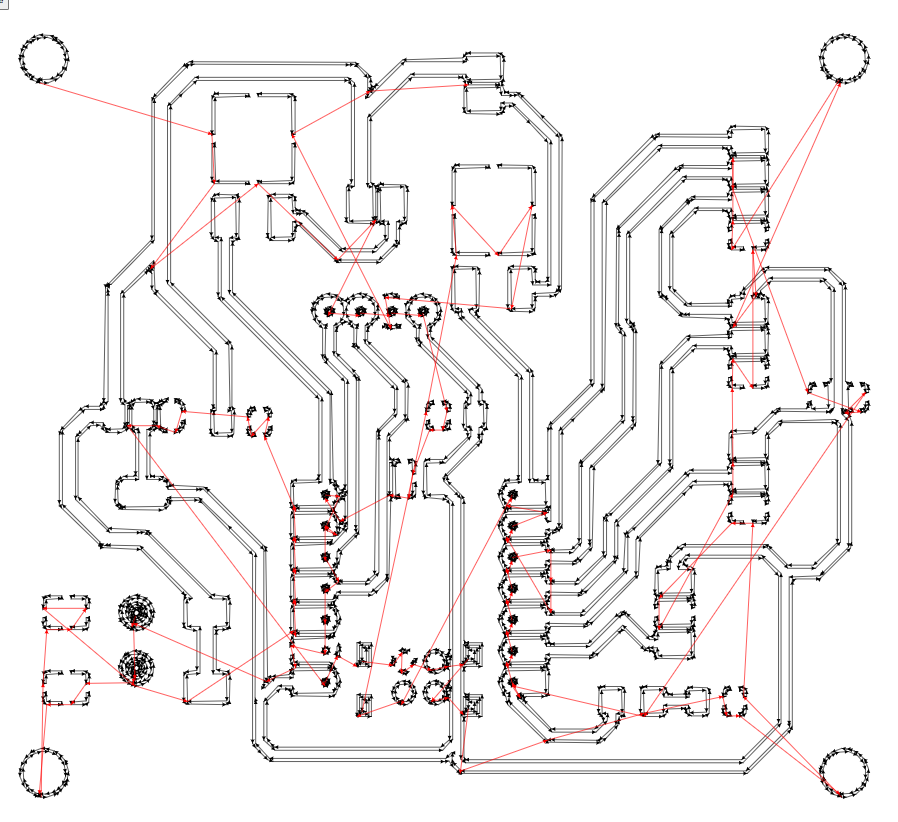
I reviewed the generated toolpath in the preview (3), where the milling paths on the PCB were clearly visible. The red lines represent the tool movements between different areas.
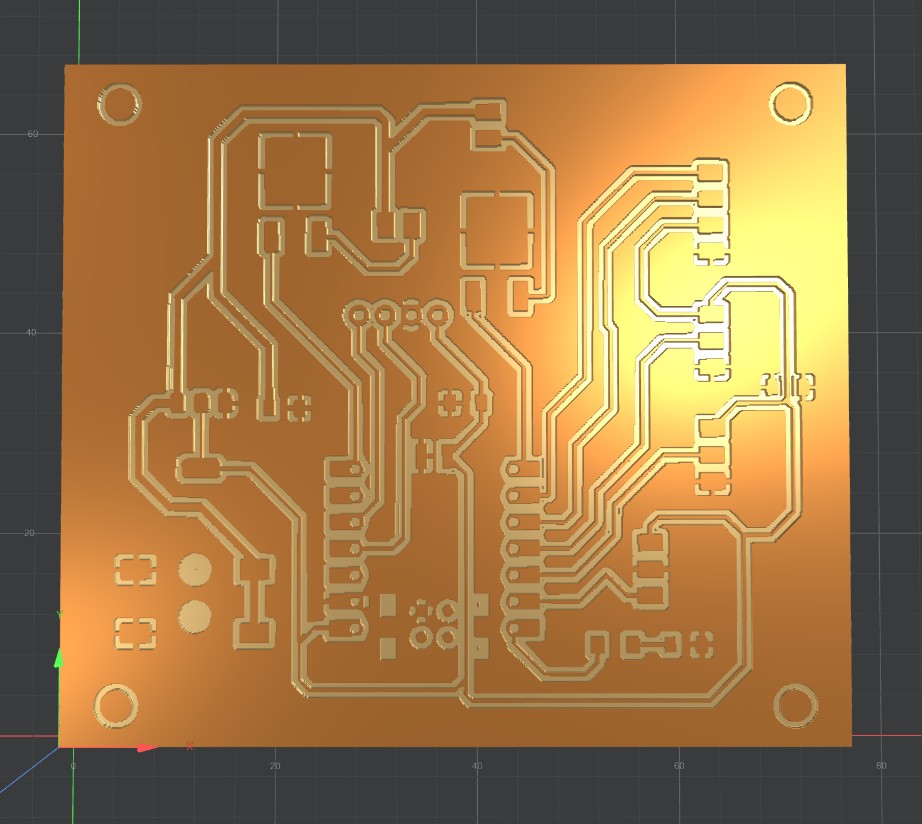
In addition, I checked the 3D view, which allowed me to visualize how the material would be removed during the milling process. This step helped me better understand the depth and overall result of the machining.
Since the on/off option was already enabled, the toolpath was directly sent to the path to G-code module, where it was converted into machine-readable G-code for the CNC machine.
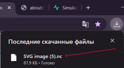
Finally, the file was saved as a .nc file, ready to be used for the milling process.
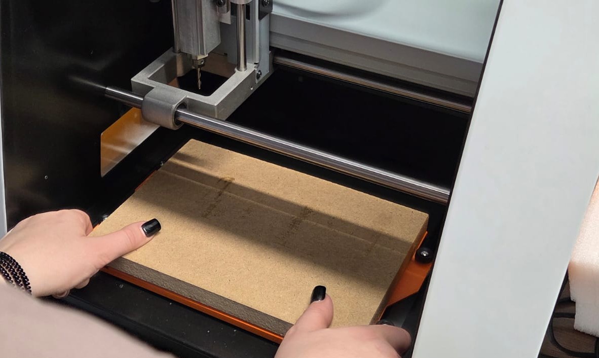
After saving the file, I moved to the milling stage using the VPanel software for the Roland SRM-20 CNC machine. First, I placed the PCB board, which had already been fixed with double-sided tape, onto the machine bed.
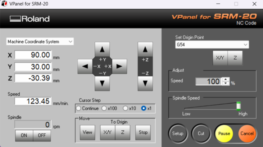
Next, I calibrated the X, Y, and Z axes to define the correct origin point for the milling process. After setting the coordinates, I loaded the generated .nc file into VPanel and started the PCB milling process.
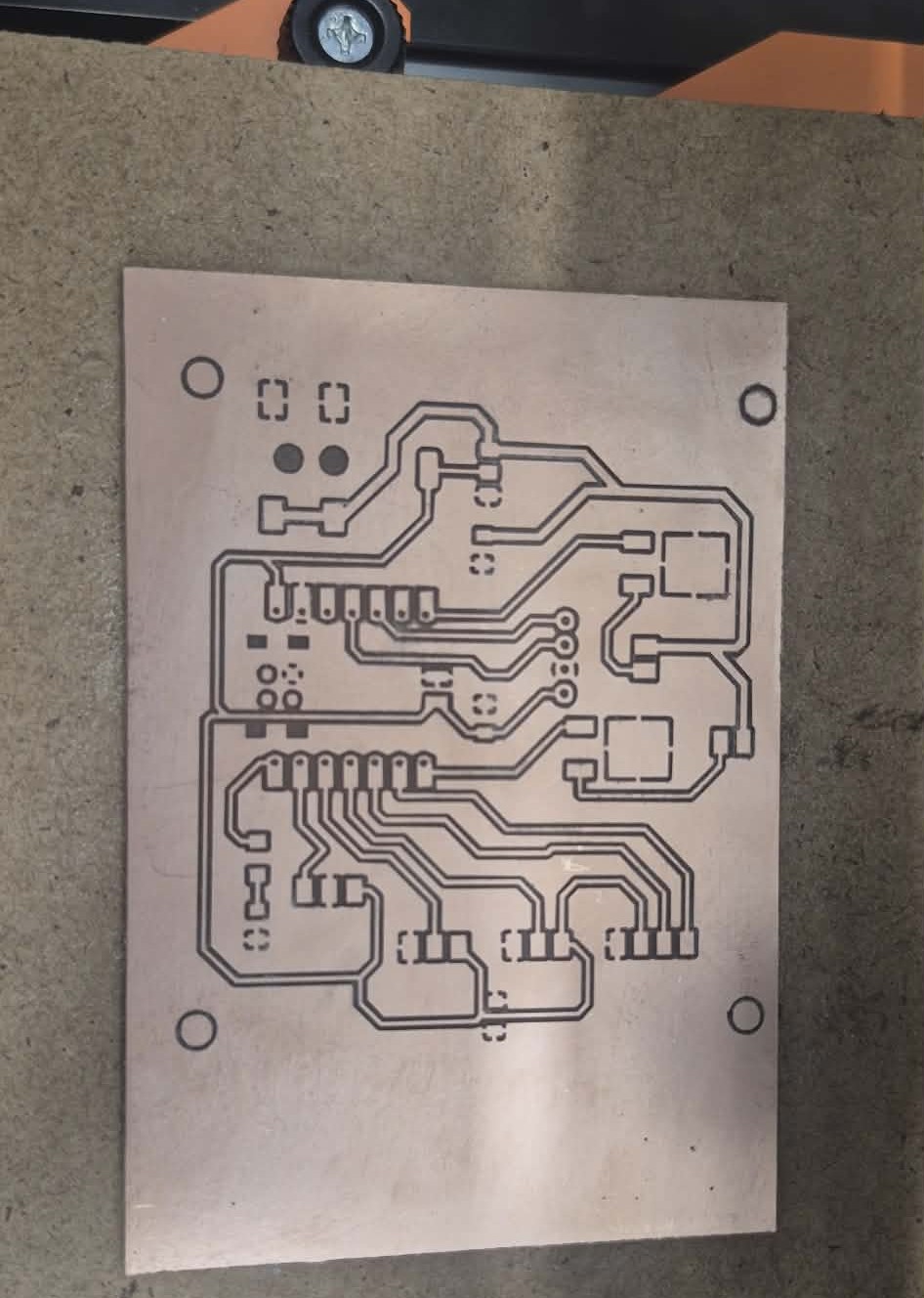
For milling the PCB traces, I used a 0.4 mm flat end mill, which provided clean and precise trace results.
After completing the first milling stage, I generated a new G-code in MODS using the same workflow, this time for cutting the board outline and creating the mounting holes with a 0.8 mm end mill.
Then, without changing the X and Y coordinates, I replaced the milling bit and recalibrated only the Z axis to correctly define the height of the new tool. After that, I loaded the saved .nc file and started the PCB outline cutting process.
PCB Assembly and Soldering
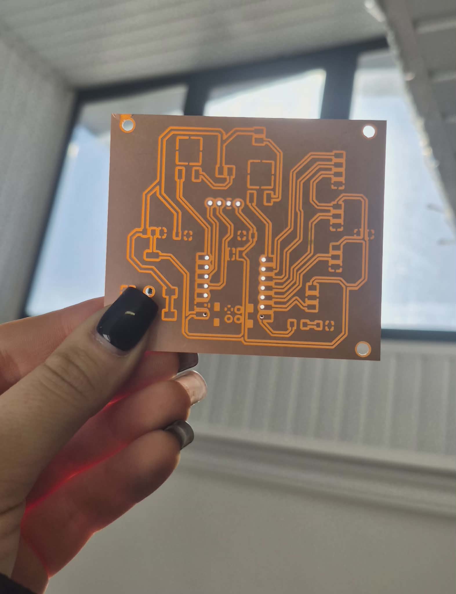
After the milling and cutting process, the final PCB was ready, with all traces clearly visible as well as the holes for component placement.
In the next stage, I proceeded with component placement and soldering. For this process, I used a Weller soldering station, set to approximately 350°C. I used 0.8 mm lead-free solder wire, and for working with small components, I used a soldering iron with a fine tip.
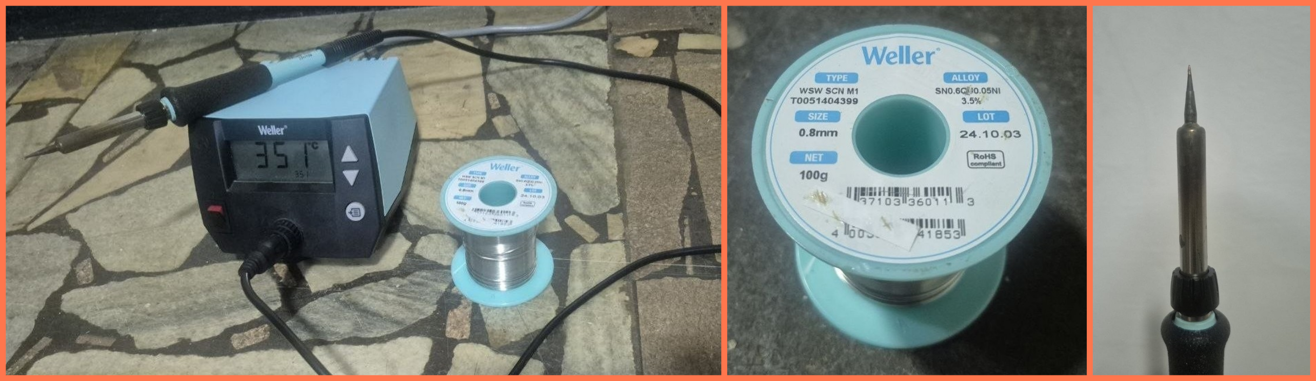
During soldering, I first placed the smaller and more sensitive components, then moved on to the larger parts. After placing each component, I checked the soldering quality to avoid weak joints or short circuits.
Special attention was required for soldering the Seeed Studio XIAO RP2040 microcontroller, since its pins are positioned very close to each other. During soldering, it was discovered that the power jack had been installed in the opposite orientation. This helped highlight the importance of carefully checking component polarity and footprint orientation before assembly.
After completing the soldering work, I performed a final visual inspection and cleaning. All traces, solder joints, and component placements were checked to verify that everything was correctly assembled.
The final assembled board includes the XIAO RP2040 microcontroller, MOSFETs, a power connector, and pin headers for connecting external devices.
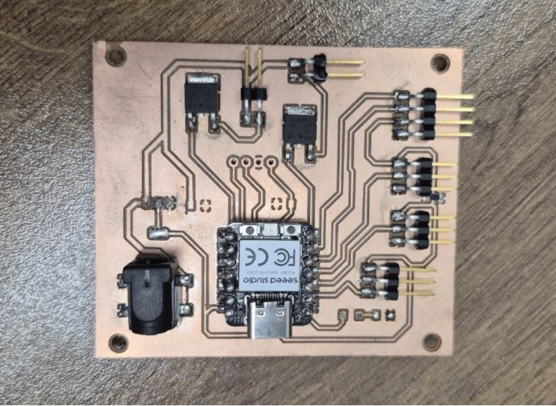
As a result, I obtained a fully assembled and functional PCB, with all components successfully placed and soldered. The board was ready for programming and further testing.
Board Functionality Test After Soldering
After completing the soldering and assembly process, it was important to verify that the board was functioning correctly and that all critical connections had been made successfully. As an initial hardware validation step, a 5V LED was connected to one of the GPIO output pins of the XIAO RP2040 board. A simple test program was then uploaded to configure the selected pin as an output and set it to a HIGH state.
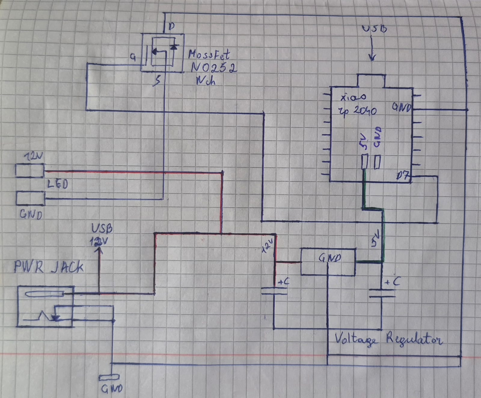
const int ledPin = D7;

void setup() {
  pinMode(ledPin, OUTPUT);
  digitalWrite(ledPin, HIGH);
}

void loop() {
}
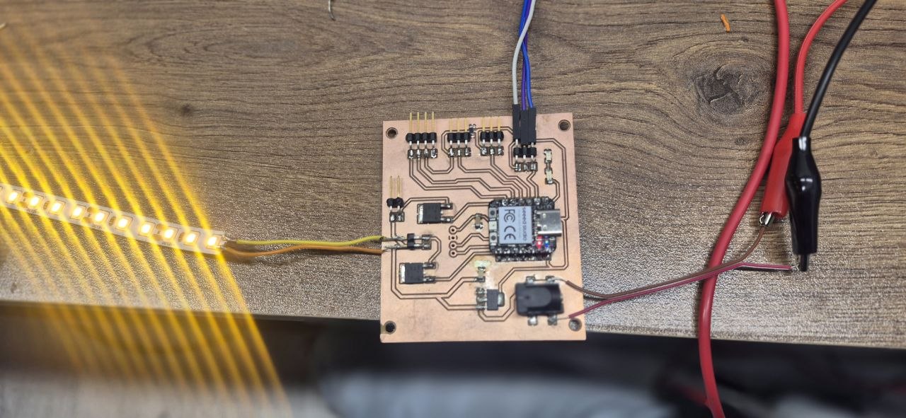
The LED illuminated continuously after uploading the code, indicating that the board was receiving power and that the microcontroller was able to control the output pin correctly.
LED Strip Testing and MOSFET Issue
During further testing of the LED strip, it was observed that it behaved only as a simple ON/OFF output and did not respond to software-based dynamic control such as blinking or fading.
After investigation, it was found that the issue was caused by an incorrect MOSFET connection. This mistake originated during the Week 6 schematic design, where the N-channel MOSFET was incorrectly wired as follows:
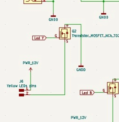
- Drain and Source pins were swapped
- Required gate resistors (pull-down or limiting resistors) were missing
- The MOSFET’s internal body diode allowed current flow even in the OFF state
- As a result, the MOSFET did not function as a proper software-controlled switch and did not respond to PWM or ON/OFF control
This limitation meant that the intended functionality could not be achieved, which required a full schematic revision and a new board design.
To better understand the cause of the problem, I studied a standard N-channel MOSFET low-side switching circuit. This reference helped me understand the correct Drain, Source, and Gate connections, as well as the purpose of the gate resistor and pull-down resistor. By comparing it with my own schematic, I was able to identify the design mistakes more clearly and determine the necessary changes before redesigning the PCB.
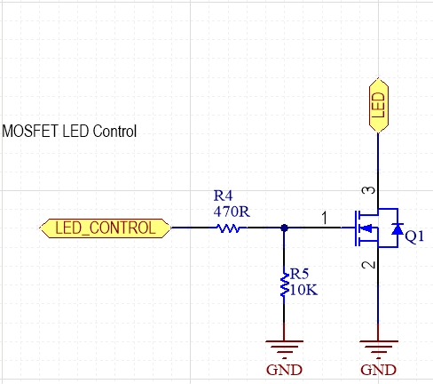
Image source:Electrical Engineering Stack Exchange, “N-channel MOSFET LED driver issue with PMV13XNEAR”
After identifying the issue, I reviewed the schematic and during Week 9 corrected the N-channel MOSFET connection by ensuring proper Drain and Source placement, and adding the required gate control resistors.
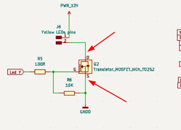
As a result, the LED strip could finally be controlled reliably and fully through software.
SMD LED Testing
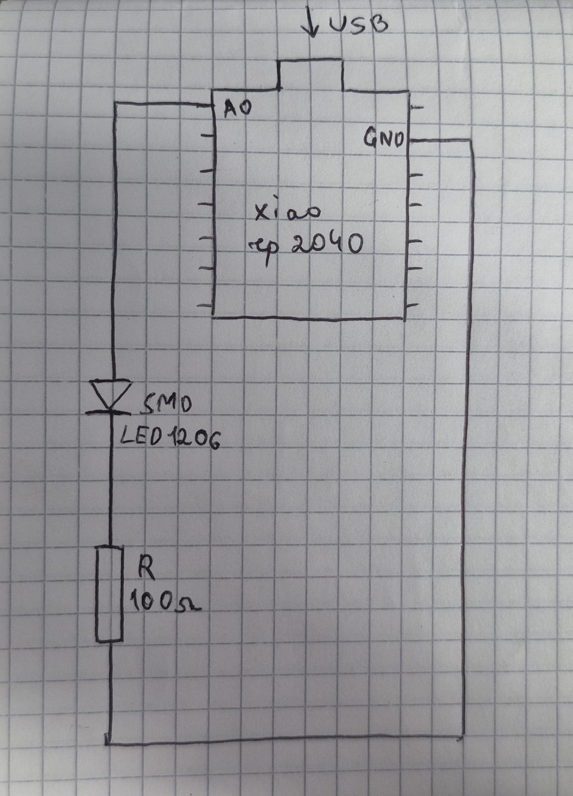
Since my board already included an onboard SMD LED,
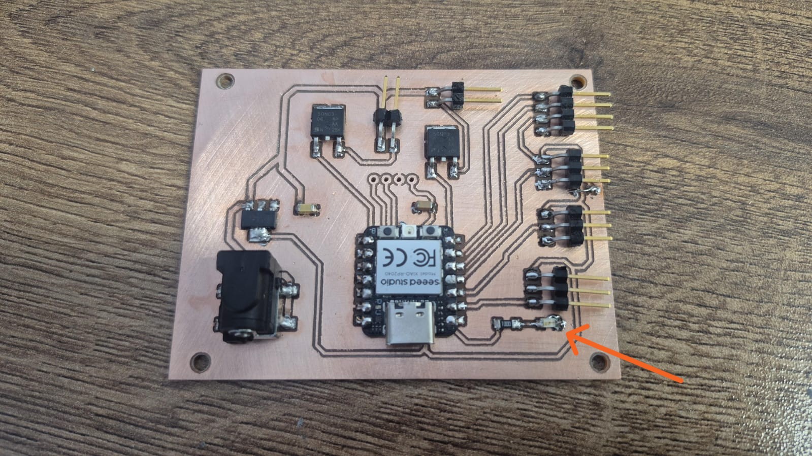
I decided to test its behavior under software control. I used a simple program where the LED turned ON and OFF every 5 seconds.
const int ledPin = A0;

void setup() {
  pinMode(ledPin, OUTPUT);
}

void loop() {
  digitalWrite(ledPin, HIGH);
  delay(500);
  digitalWrite(ledPin, LOW);
  delay(500);
}
This test showed that the LED responds correctly to digital signals and can reliably switch states according to the program.
Fade In Experiment
I also tested a second program implementing a fade-in effect. Using PWM signal modulation, the LED brightness gradually increased, creating a smooth lighting transition.
const int ledPin = A0;

void setup() {
  pinMode(ledPin, OUTPUT);
}

void loop() {
  for (int i = 0; i <= 255; i++) {
    analogWrite(ledPin, i);
    delay(10);
  }

  for (int i = 255; i >= 0; i--) {
    analogWrite(ledPin, i);
    delay(10);
  }
}
During the experiment, the LED brightness slowly increased from 0 to maximum intensity, creating a smooth transition effect. After reaching full brightness, the program then decreased the brightness back down, demonstrating a complete fade cycle. This behavior showed that the LED can support analog-style control through PWM and can produce smooth visual effects instead of simple digital switching.
LDR Sensor Integration
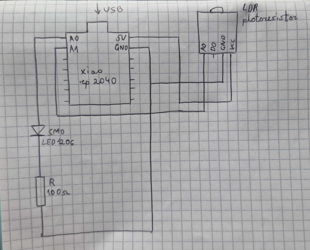
Since my board also included an LDR (Light Dependent Resistor) sensor, I decided to integrate it with the SMD LED to create an automatic light-controlled system. The LDR was connected to an analog input pin, while the LED was connected to a digital output.
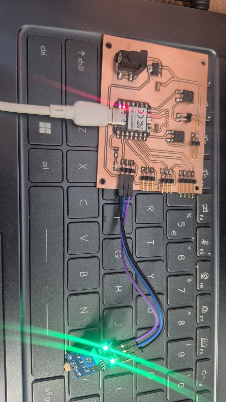
During testing, it was observed that when the LDR was covered or the environment became dark, the sensor values changed and the LED turned ON. In the presence of light, the LED turned OFF.
const int ledPin = A0;
const int ldrPin = A1;

int threshold = 300;

void setup() {
  pinMode(ledPin, OUTPUT);
}

void loop() {
  int lightValue = analogRead(ldrPin);

  if (lightValue > threshold) {
    digitalWrite(ledPin, HIGH);
  } else {
    digitalWrite(ledPin, LOW);
  }

  delay(50);
}
This experiment demonstrated the basic principle of an automatic control system, where sensor input directly affects the output behavior.
Conclusion
This week provided a complete hands-on experience of the PCB manufacturing process, from design preparation in KiCad to fabrication using the Roland SRM-20 CNC machine and final assembly. It helped me understand the full workflow of turning a digital design into a physical, functional board.
During testing, the board successfully demonstrated basic GPIO control, confirming correct operation of the core system. However, issues in the LED strip circuit revealed a design problem related to an incorrect MOSFET connection, which prevented proper switching and dynamic control.
This issue became an important learning outcome, highlighting the importance of careful schematic design, correct component placement, and verification before fabrication. Overall, the process strengthened my understanding of PCB production as an iterative workflow that involves continuous testing, debugging, and improvement.