Week 15 . System Integration
Final Project Structure
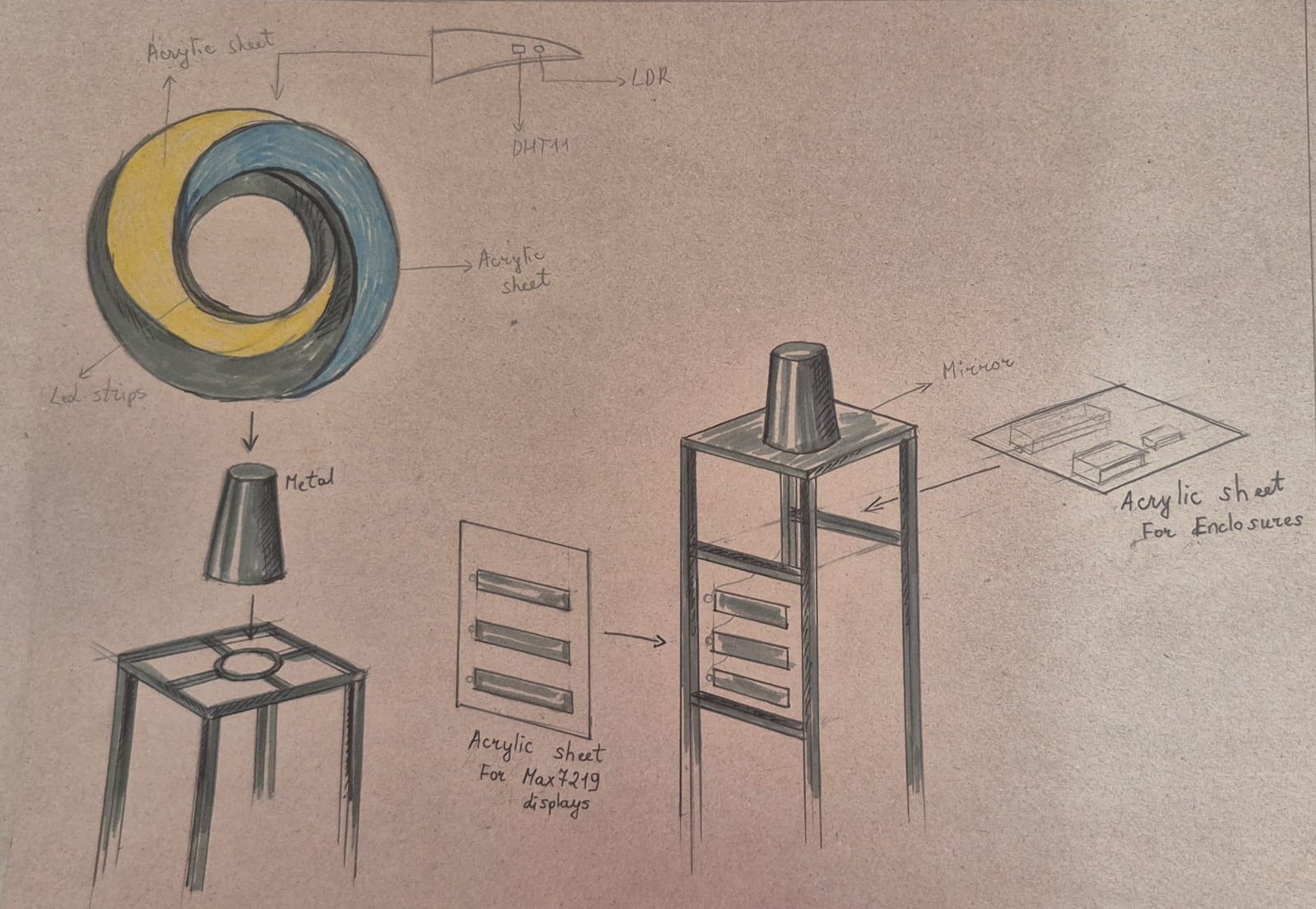
The structure of my final project was developed through a combination of CAD modelling, hand-drawn sketches, physical fabrication, and design modifications made throughout the development process.
Since the project developed through an iterative and experimental process, I did not create a complete 3D model of the entire final structure from the beginning. The parts that required precise digital modelling were designed using FreeCAD. However, the upper structural elements were developed through sketches, physical fabrication, and continuous modifications during the construction process.
At the time of this week, the metal structure was already partially fabricated, but its final version had not yet been completed. Since the upper section was still being modified and adapted to the actual physical conditions, creating a complete 3D model of this part was not necessary at that stage and would not have represented the final structure.
Instead, I focused on designing and fabricating the parts that could be practically developed at that stage, as well as adapting the structure according to the actual physical conditions and assembly requirements. This approach allowed me to focus my time on the actual fabrication, assembly, testing, and development of the project rather than creating a complete 3D model of a structure that was still continuously changing.
Therefore, the final project structure was developed progressively by combining the existing CAD model, sketches, physical fabrication, testing, and continuous design modifications.
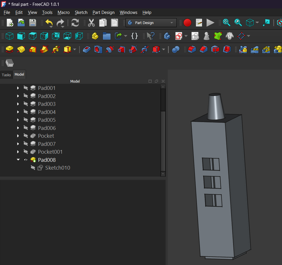
The initial CAD modelling of the lower section of the project was carried out during Week 2 as an initial development of the structural foundation of the project. During the System Integration stage, this previously developed model was used as part of the overall project structure and as a basis for further physical fabrication.
During the fabrication of the metal components, design decisions were checked and adapted according to the actual physical conditions. This process included cutting and further preparation of the metal parts according to the developed design.
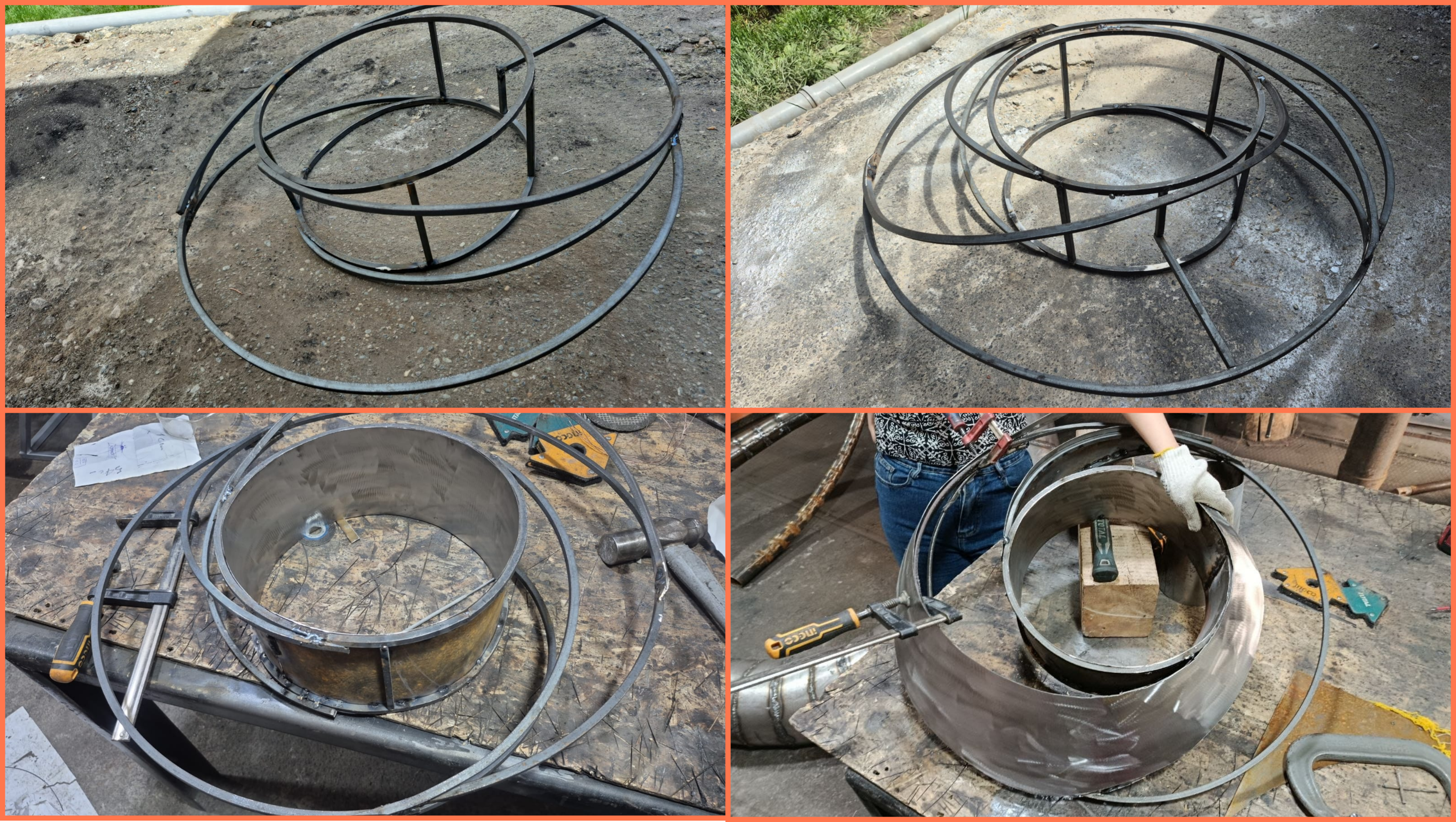
This approach allowed the design to be adapted to the physically fabricated components and the requirements of the final assembly. Since some parts of the project were developed directly during the physical fabrication process, the design was continuously adjusted according to the actual dimensions, structure, and assembly conditions.
As a result, the structure of the final project was developed progressively through a combination of digital design, sketches, physical fabrication, and testing.
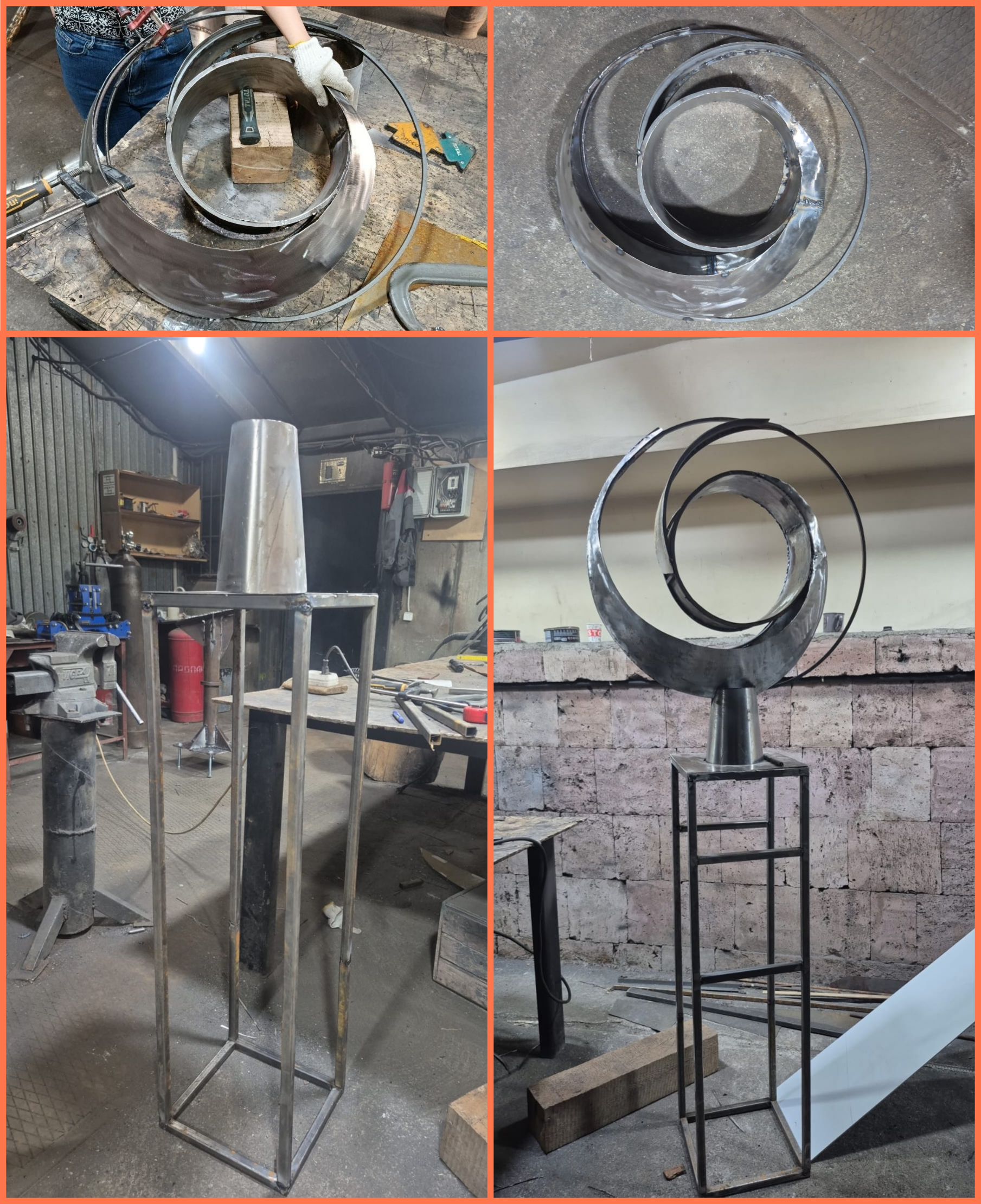
The following documentation shows the development of the project structure through the available CAD models, sketches, metal fabrication, and physical assembly.
Enclosures and Mounting Structures
After developing the overall structure of the project, the next step was to design protective enclosures and mounting structures for the individual components of the system. Since the final system includes several electronic and power modules, it was necessary not only to ensure their safe operation but also to organise their secure installation, protection, and connection to the overall structure.
Each enclosure and mounting structure was designed according to the dimensions and requirements of the corresponding component. Mounting points, cable openings, ventilation openings, and other structural features were incorporated to ensure the safe and organised integration of the system.
This section presents the design and fabrication process of the enclosures and mounting structures developed for the main control board, power supply unit, voltage regulator, and LCD displays.
The first enclosure was designed for the main board, which serves as the central control unit of the system. It coordinates the operation of the different modules, processes data received from sensors, and controls the output devices. Therefore, it was important to design a protective and organized enclosure that would ensure the safe installation of the board and provide convenient access for wiring and connections.
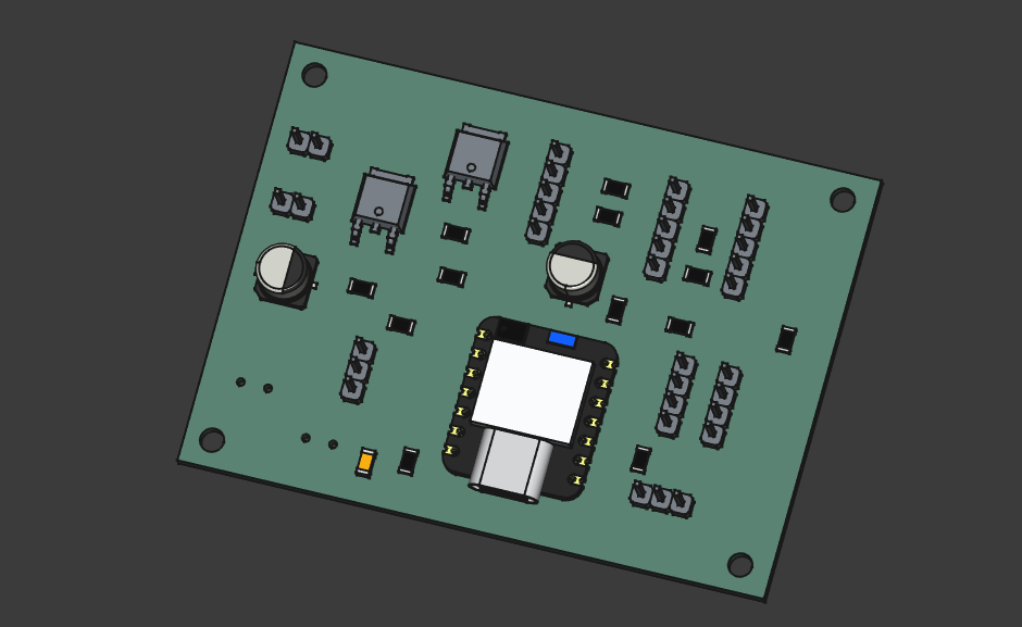
At the beginning, I exported the STEP-format 3D model of my board from KiCad, then imported it into FreeCAD and used it as a reference model.
The design process was carried out in stages, since the enclosure was intended to have a closed structure.
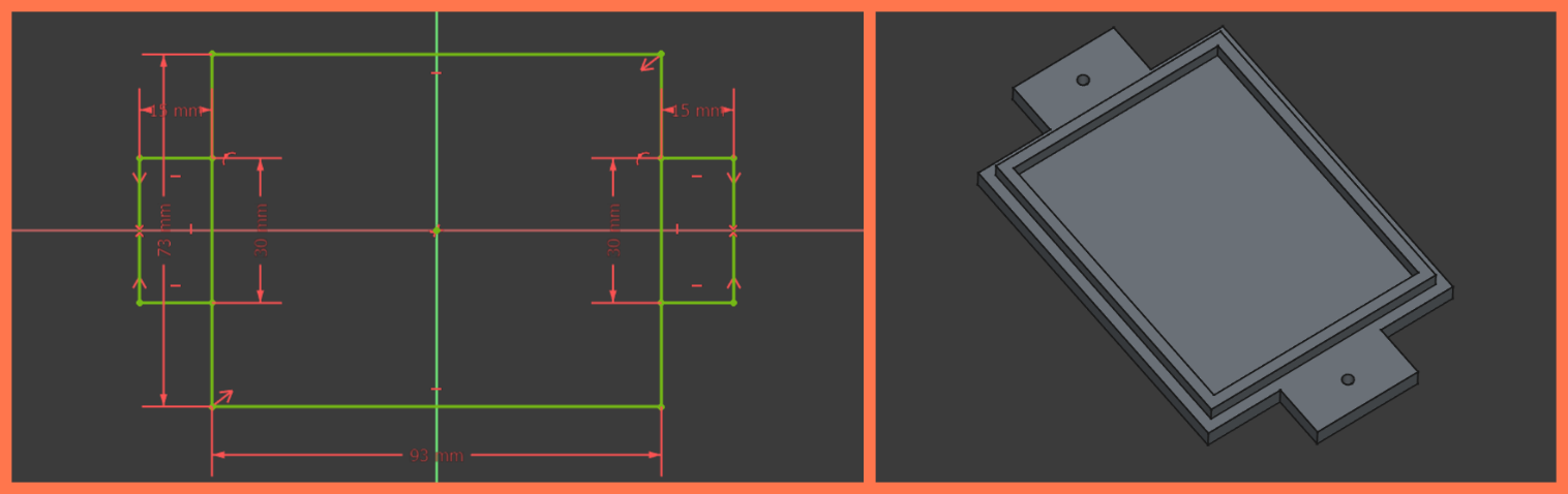
First, while designing the bottom part of the enclosure, I added extended mounting tabs on the sides so that the box could later be attached to the main structure using bolts and nuts.
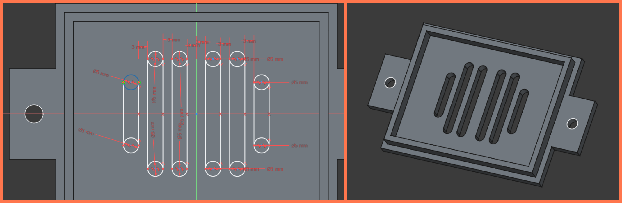
Then, I added ventilation holes to the bottom part of the enclosure to ensure air circulation and prevent possible overheating of the electronics.
Finally, I designed the board mounting holes, taking into account the actual dimensions of the board and its mounting points, so that it could be properly and securely fixed inside the enclosure.
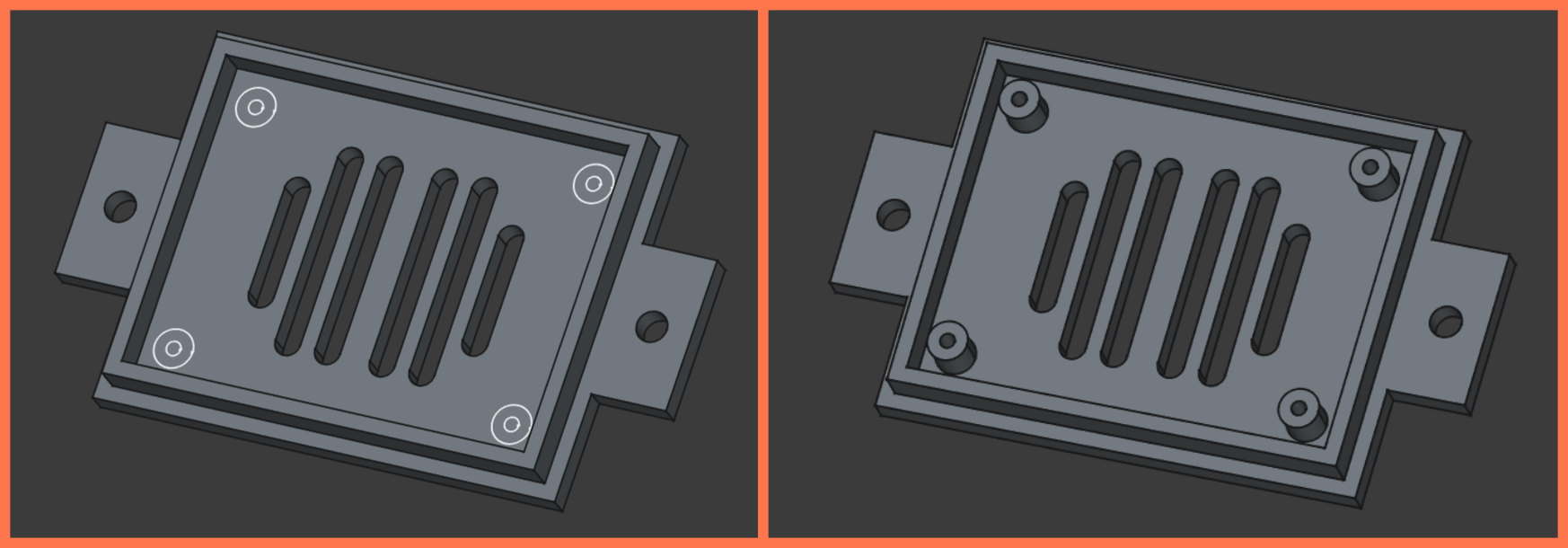
Then, I placed the board onto the designed base to check whether all dimensions, mounting holes, and clearances matched correctly.
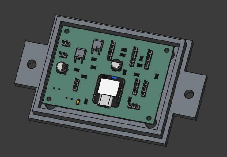
The next step was designing the lid, which I designed in a way that it would fit tightly with the inner part using an interlocking mechanism, ensuring a stable and reliable closed structure of the enclosure.
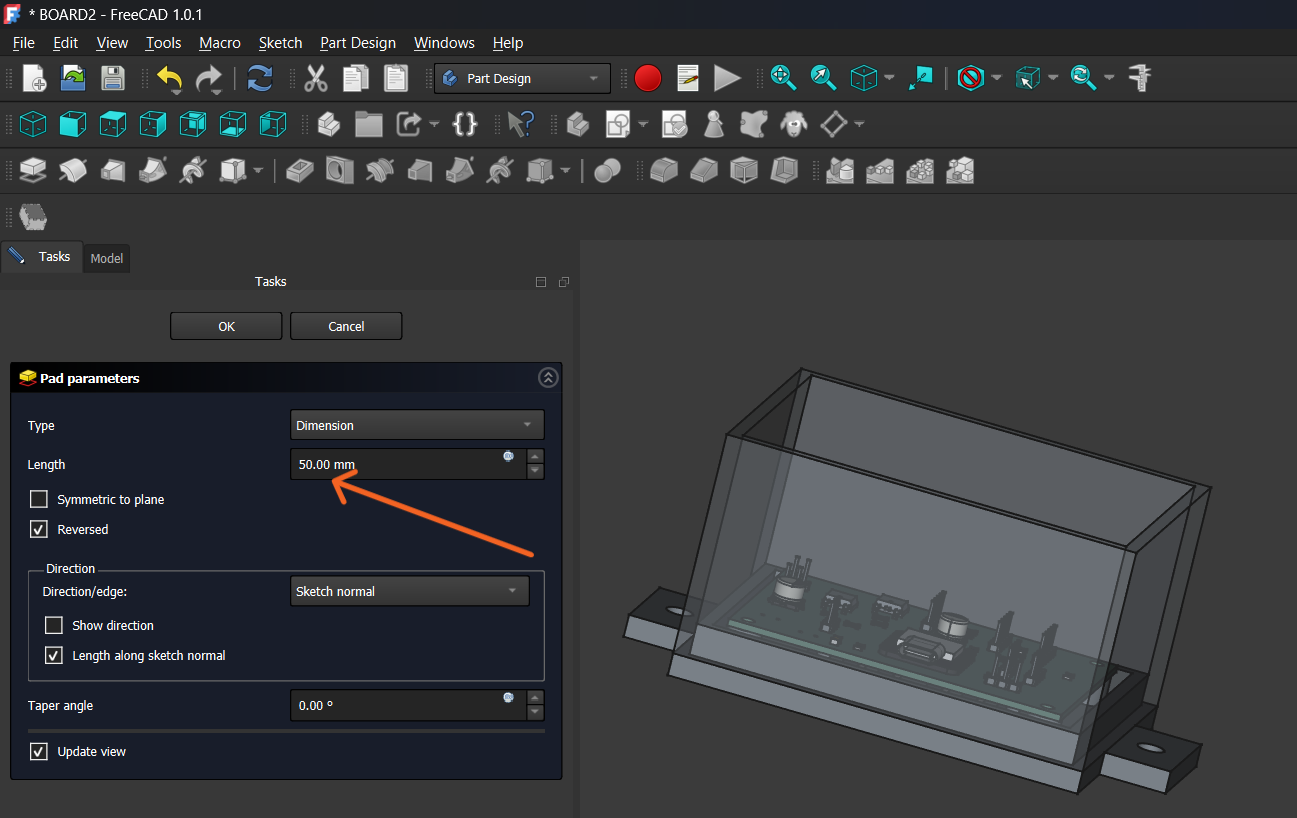
Then I defined the height of the box so that during later connections there would be enough space for the wires and they would not bend.
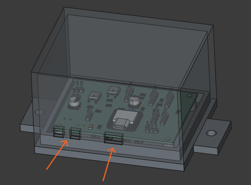
After that, I added three openings on the front side of the box: one for the 12V power cable connection, another for the 5V power supply, and the third for routing the microcontroller cable.
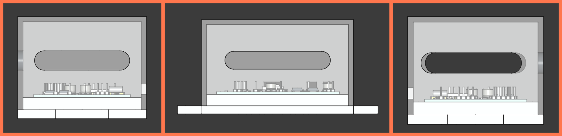
In addition, I also added openings on the remaining three sides of the box so that it would be easy to connect the wiring for sensors and other external components.
Then I decided to add the Fab Lab Armenia logo on the box as a design and project identity element, as well as to give it a more complete and professional appearance. After printing, I plan to fill the logo cutouts with epoxy resin using the original logo colors, in order to achieve a more expressive and aesthetic result.
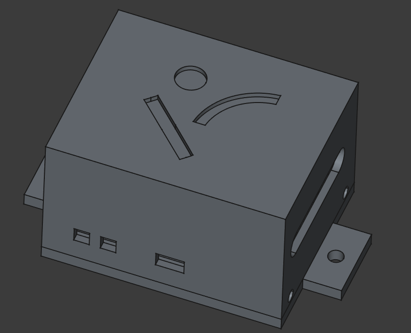
After completing the design, I saved all parts in STL format so I could import them into Orca Slicer for 3D printing preparation.
I opened the STL files separately in Orca Slicer in different windows. First, I rotated the lid so that it would sit flat on the build plate, since placing it in any other orientation would require a much larger amount of supports. I chose tree type supports to ensure a more stable structure and easier removal during printing.
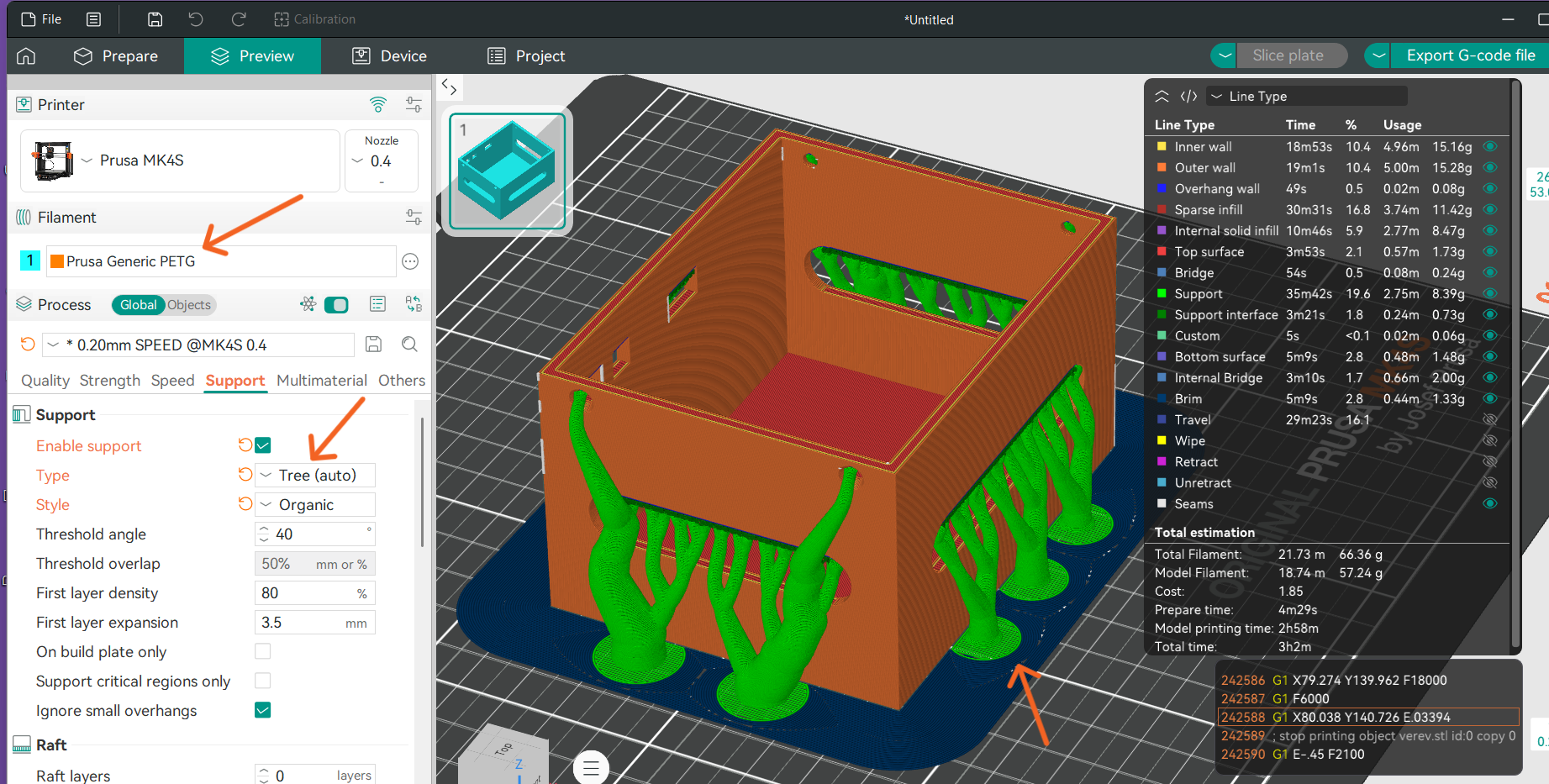
The bottom part did not require supports, since it was fully resting on a flat surface and did not include any overhanging elements.
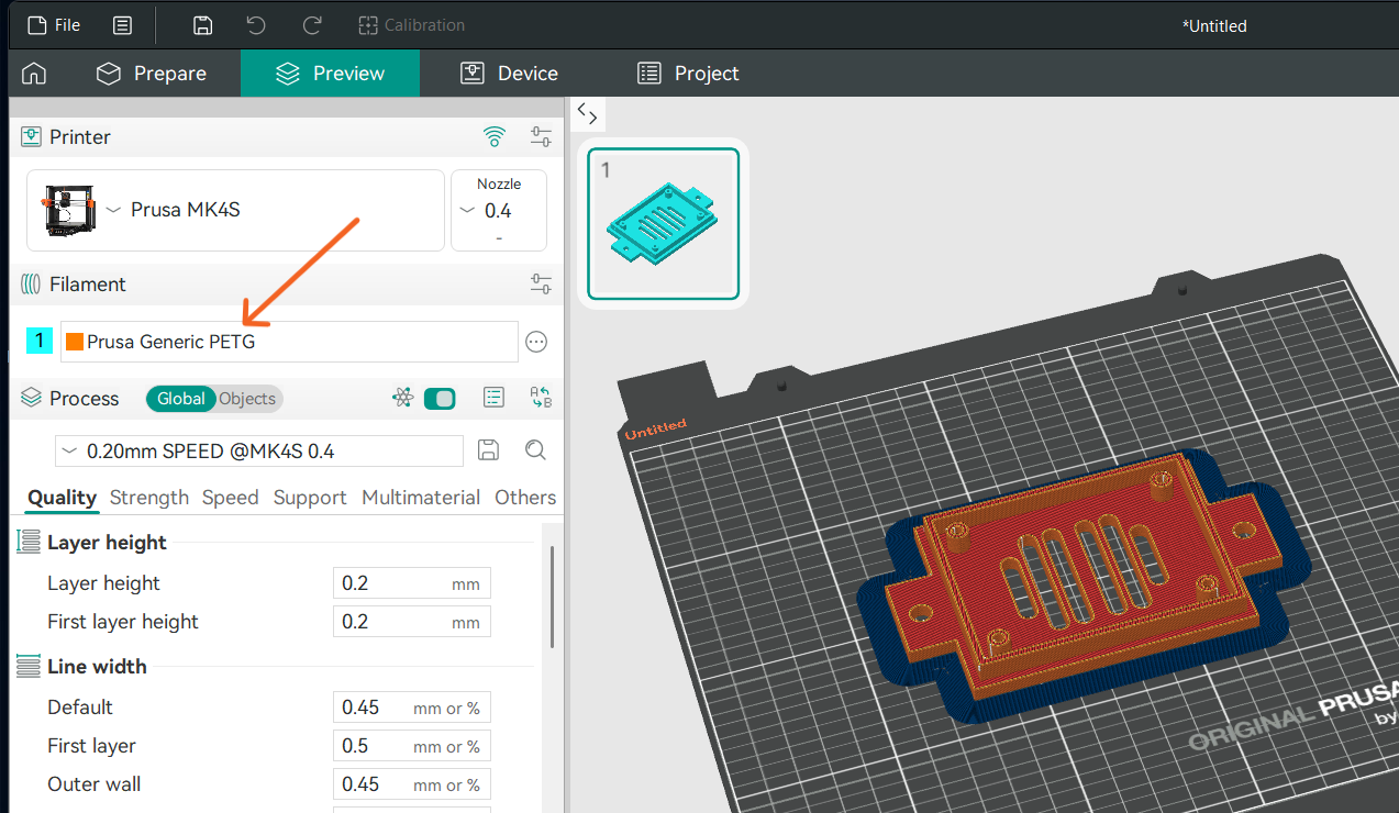
I generated both parts using Generic PETG material and sent them for printing.
I printed the bottom part in black color, and the lid in vanilla white PETG. The choice of colors was made purely for design and aesthetic combination purposes.
While the main board enclosure was being printed, I moved on to designing the enclosure for the power supply unit.
The next enclosure was designed for the power supply, which is responsible for providing power to the entire system and distributing energy to the different electronic modules. Since the power supply can generate heat during operation, it was important to ensure both secure mounting and adequate ventilation. For this reason, the enclosure was designed with mounting features, cable routing openings, and ventilation holes to support safe and reliable operation within the overall system.
Power Supply
I measured all the dimensions and started designing the model based on those measurements.
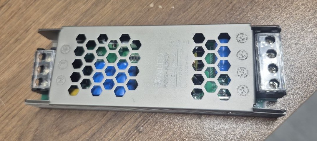
As with the motherboard case, I added protruding mounting “tabs” on the sides,as well as prepared mounting holes to securely and stably fix the power supply.
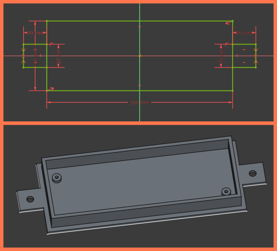
I added ventilation holes on the lid to ensure air circulation and prevent possible overheating.
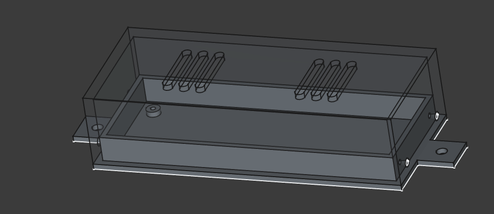
I added rectangular openings in the side sections for wiring connections, as well as two mounting holes so that the box could be secured with screws.
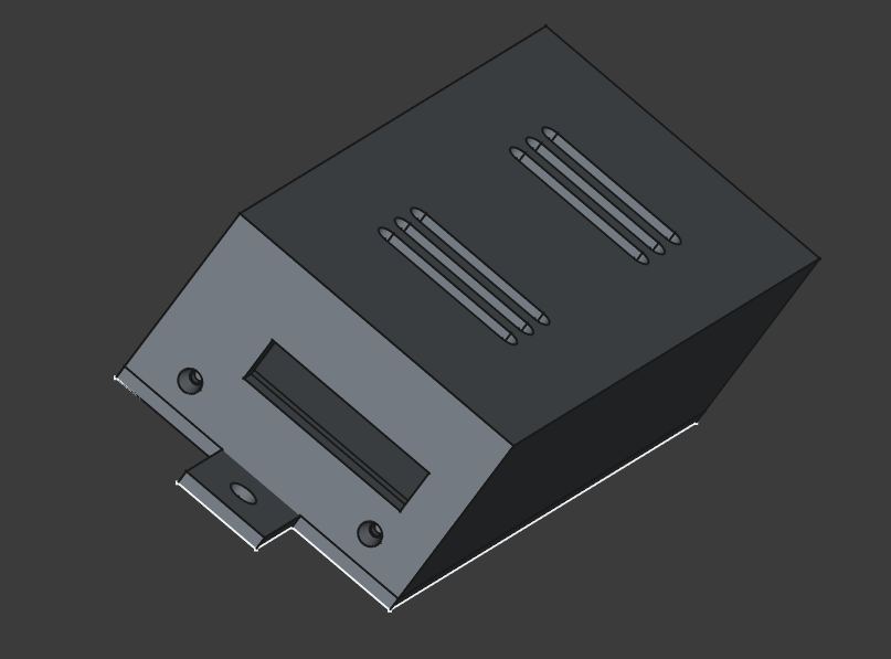
Thus, this part was also ready for printing. As with the board enclosure, I used the same settings for this box as well. The only difference was that I printed the lid using transparent PETG filament.
Voltage Regulator
The next enclosure was designed for the voltage regulator. The role of this module is to convert the input voltage and provide the stable voltage required by the different components of the system. Since the voltage regulator is an important part of the power distribution chain, it was necessary to ensure its safe placement and organized integration within the overall system.
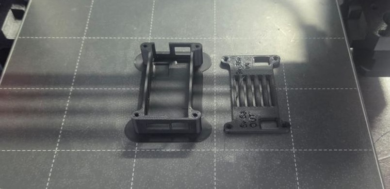
For this purpose, I searched online and found a suitable 3D model that matched the voltage regulator used in my project. I imported it into my design environment and, without making any modifications, prepared it for 3D printing. The model was then sent for fabrication as a dedicated enclosure for the voltage regulator.
LCD Mounting Structure
The displays serve as the primary interface between the system and the user, as they are responsible for presenting the system information. Therefore, it was necessary to design dedicated mounting structures that would ensure proper positioning and reliable fixation of the displays.
In addition to this, the displays needed to be mounted onto the acrylic sheet located behind the mirror. However, attaching the displays directly to the acrylic sheet was neither a convenient nor a reliable solution. For this reason, I decided to first create a 3D model of the mounting structure. I began by measuring the exact dimensions of the displays and used those measurements as the basis for the design. Next, I designed the mounting holes: first the holes used to attach the displays to the mount, and then the holes used to secure the entire structure to the acryl sheet.
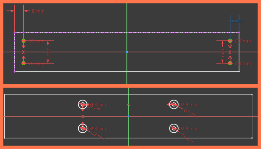
This approach made it possible to accurately define the position, angle, and spacing of the displays. As a result, the system could be designed in a more controlled manner while ensuring that all displays would be correctly aligned and securely fixed during the final assembly process.
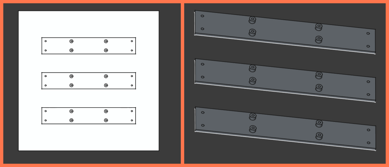
After the modeling was completed, I prepared the parts for 3D printing by generating G-code in the slicer software. I chose transparent PETG filament as the material. First, I printed a test piece to verify that all dimensions, holes, and mounting points were correct.
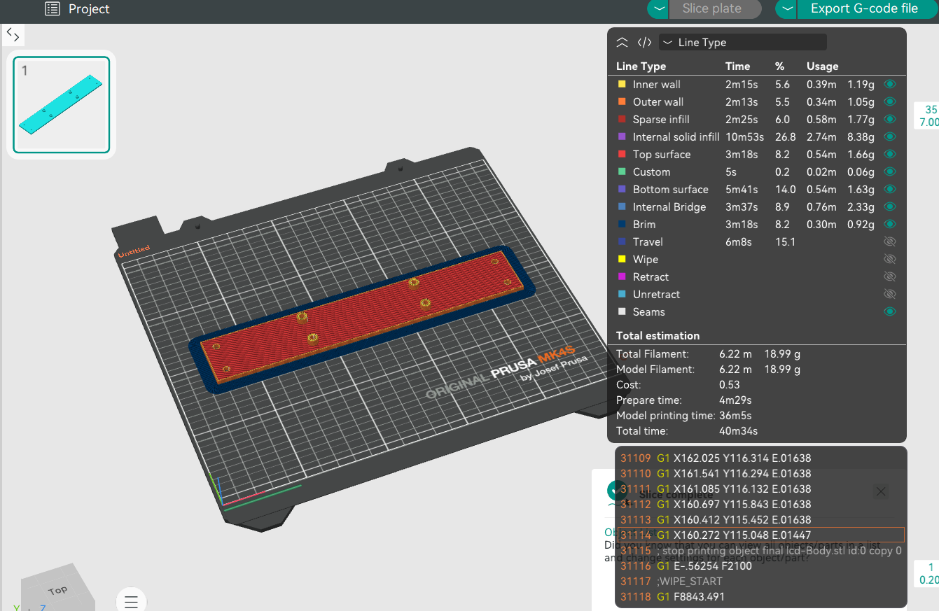
After confirming that the design worked as intended, I printed two additional parts, since the project uses three displays in total and each display required its own mounting structure.
Mounting and Fastening
All enclosures and mounting structures were designed with dedicated mounting tabs and mounting holes so that they could be securely attached to the main structure using screws, bolts, and nuts. The PCB, power supply, and LCD displays also have dedicated mounting points to ensure their stable and secure installation. This modular fastening approach simplifies system assembly, maintenance, and disassembly when necessary.
Electronic System
The electronic system of my final project is built around a custom-designed PCB that I designed and fabricated during Week 9. The board is based on the Seeed Studio XIAO RP2040 microcontroller and serves as the central control unit of the entire system. During Week 9, I designed the schematic, created the PCB layout, manufactured the board, assembled all the components, and verified its functionality.
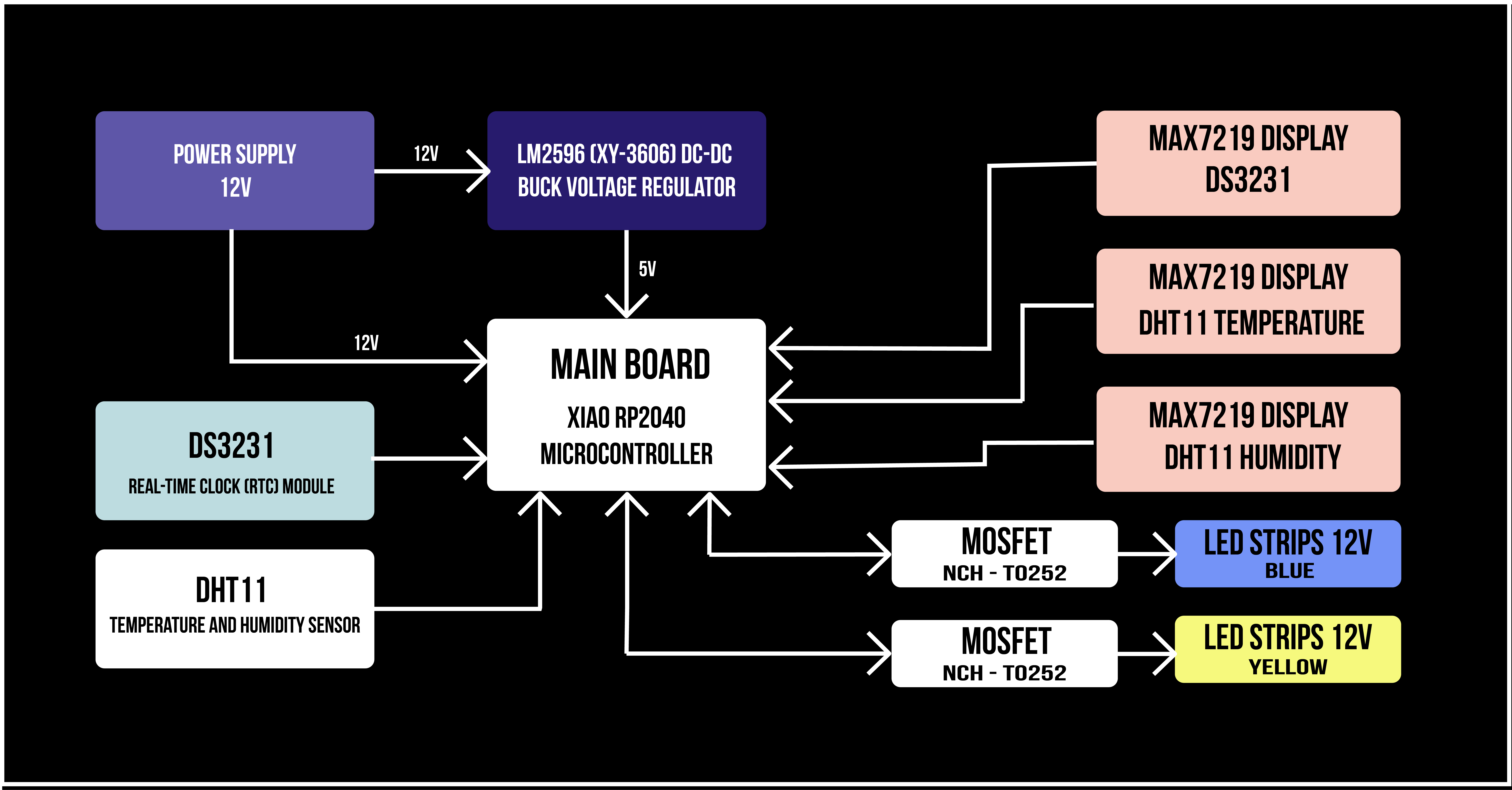
In the final project, this PCB is responsible for coordinating all electronic modules. It reads data from the sensors, communicates with the DS3231 Real-Time Clock (RTC) module, controls the MAX7219 LED matrix displays, and switches the 12 V LED strips through MOSFET drivers. All electronic modules are connected to the main PCB, forming a single integrated electronic system.
Electronic System Block Diagram
To better illustrate the overall operation of the project, I created a complete block diagram of the electronic system. The diagram shows how the power supply, the main PCB, sensors, RTC module, LED matrix displays, and LED strips are interconnected, providing a clear overview of the communication and power distribution throughout the system.
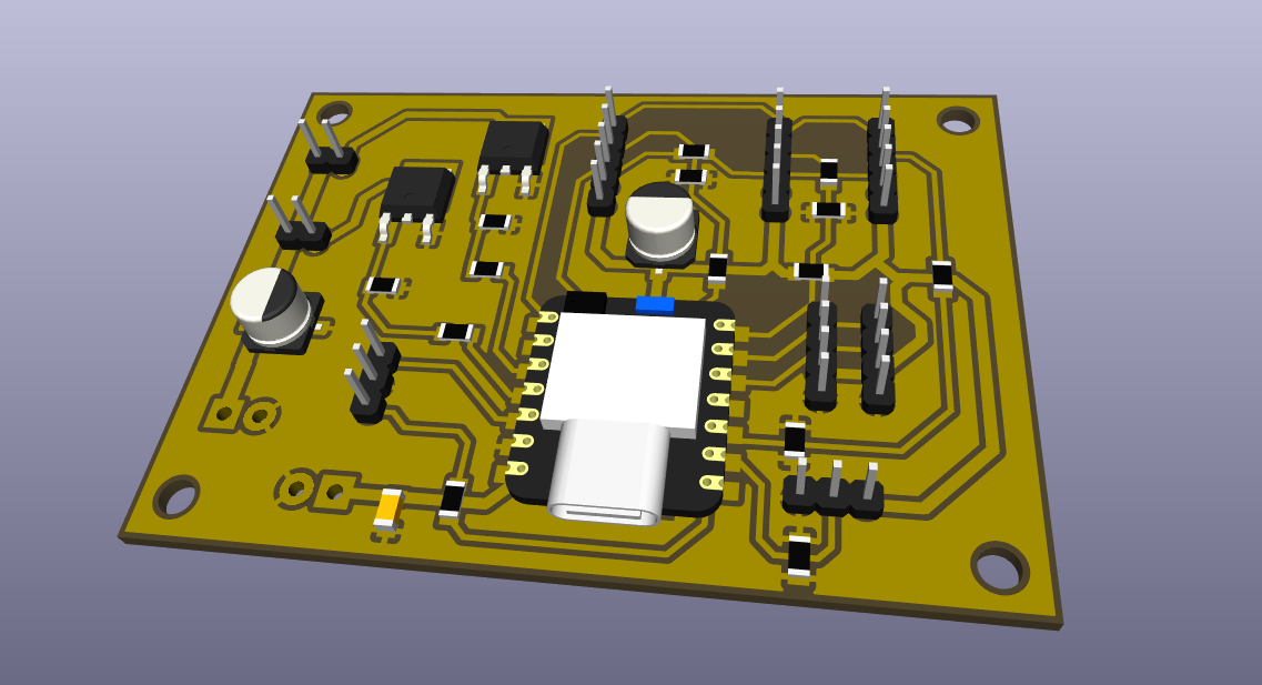
PCB 3D Model
Before manufacturing the PCB, I used the KiCad 3D Viewer to inspect the three-dimensional model of the board. This allowed me to verify the placement of all electronic components, connectors, and mounting holes before fabrication. The 3D model also helped ensure that the PCB would fit correctly inside the custom-designed enclosure without any mechanical interference.
Wiring Diagram
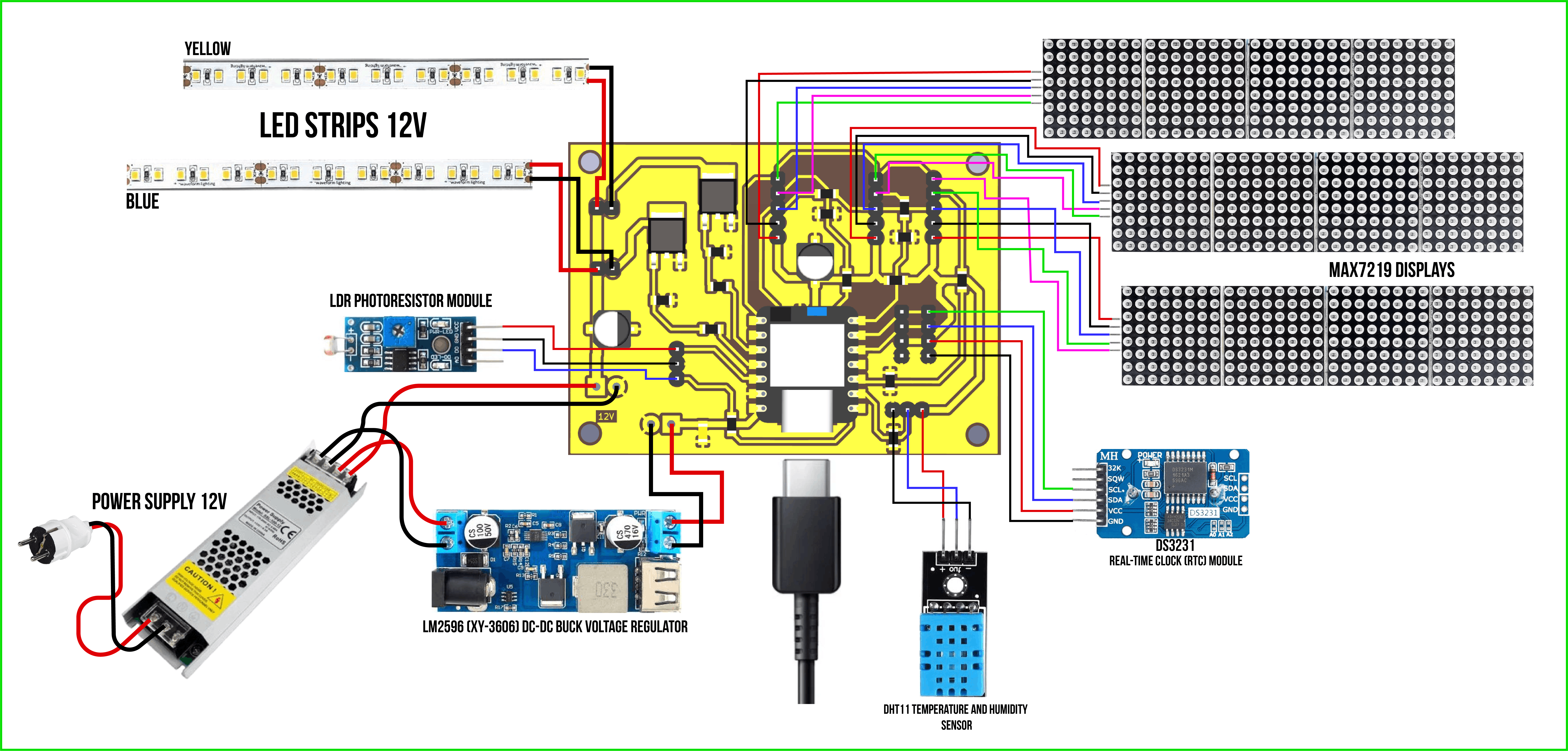
During the final system integration, I created a complete wiring diagram to document all electrical connections between the main PCB and the external modules. The diagram clearly illustrates both the power distribution and the signal connections throughout the system.
The wiring diagram includes:
- 12 V power supply
- LM2596 (XY-3606) DC-DC buck converter
- Main PCB
- Three MAX7219 LED matrix displays
- DS3231 Real-Time Clock (RTC) module
- DHT11 temperature and humidity sensor
- LDR light sensor
- Two 12 V LED strips
This diagram was used during assembly to verify all electrical connections, simplify the integration process, and make future maintenance easier.
Connectors
To simplify assembly, testing, and future maintenance, several types of connectors are used throughout the system.
- USB Type-C connector for programming and powering the Seeed Studio XIAO RP2040 microcontroller.
- 2.54 mm pin headers for connecting the MAX7219 LED matrix displays, DS3231 RTC module, DHT11 sensor, and LDR sensor.
- Screw terminal connectors for connecting the 12 V power supply to the main PCB.
- Jumper wires for interconnecting the main PCB, LED matrix displays, RTC module, DHT11 sensor, and LDR sensor.
Using removable connectors makes it easy to assemble, test, disconnect, and replace individual modules without additional soldering. This improves the reliability, maintainability, and overall integration of the electronic system.
Power System
The power system of my final project is based on a 12 V power supply, which provides the main power for the entire system. The 12 V output is used directly to power the LED strips, while the electronic components require a lower voltage.
For this purpose, an LM2596 (XY-3606) DC-DC buck converter is used as a voltage regulator. Its function is to convert the input 12 V voltage to the lower voltage required by the electronic system. This allows the 12 V lighting system and the low-voltage electronic components to be powered from the same main power source.
The power supply, voltage regulator, main PCB, LED strips, and other electronic components are interconnected as part of one integrated power system. The power distribution and connections between these components are shown in the electronic system block diagram and wiring diagram presented above.
Assembly
After fabricating all the enclosures and mounting components for the electronics, I proceeded with the assembly stage. I gradually assembled all the parts by installing them into their corresponding cases and mounting structures, in order to integrate the individual modules into a single complete and functional system.
During the assembly process, I made the necessary electrical connections between the main PCB, power supply, voltage regulator, sensors, displays, and LED strips, ensuring proper organisation of both power distribution and data connections. Each component was securely fixed in its designated position, resulting in a stable and well-organised system layout.
Before the final assembly, I also completed the design of the main board enclosure lid by filling the Fab Lab Armenia logo area with epoxy resin. The resin was applied using the original logo colors, which gave the enclosure a more expressive and aesthetic appearance.
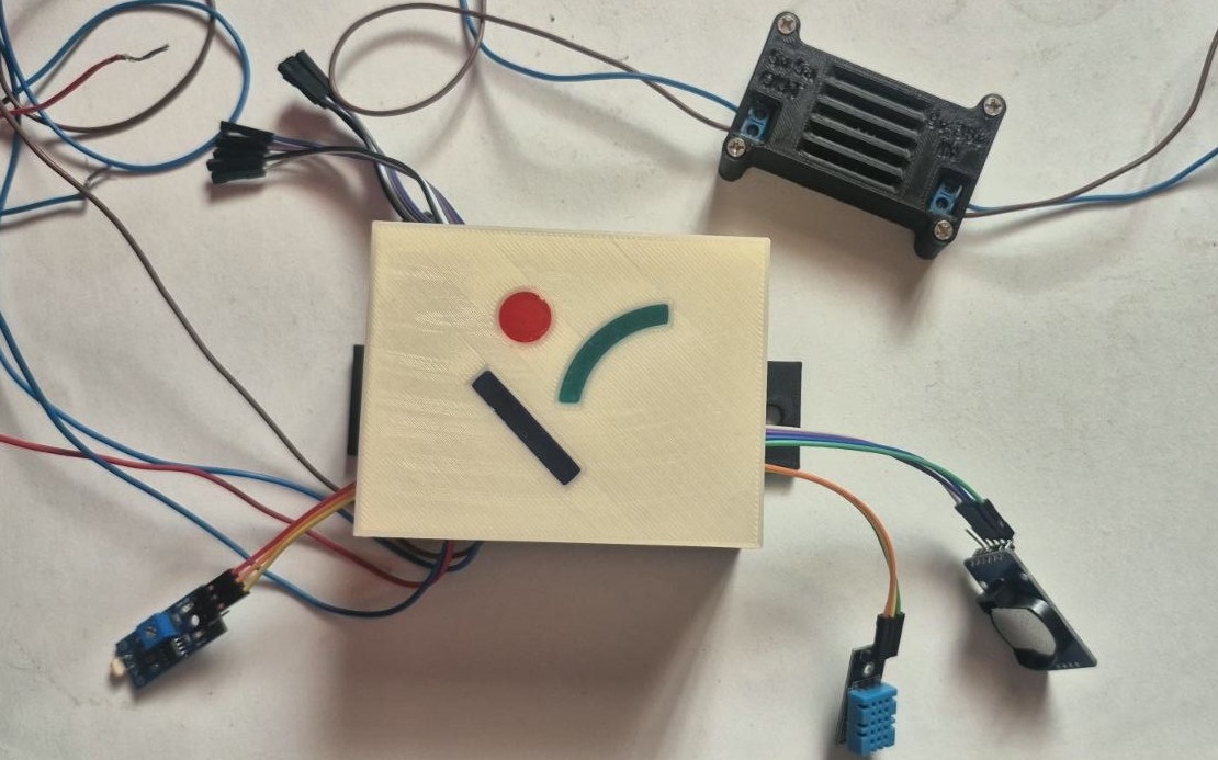
At this stage, the electronic subsystem of the project was fully assembled and tested as an independent functional system. All major electronic modules were connected and installed in their respective enclosures, forming a unified working subsystem that was ready for final integration into the mechanical structure.
Using a laser cutting machine, I cut the acrylic base for the displays. After that, I assembled the displays onto the acrylic base, aligning them with the pre-designed mounting holes and positioning to ensure correct layout and stable fixation. As a result, the display module became a solid and well-organized structure.
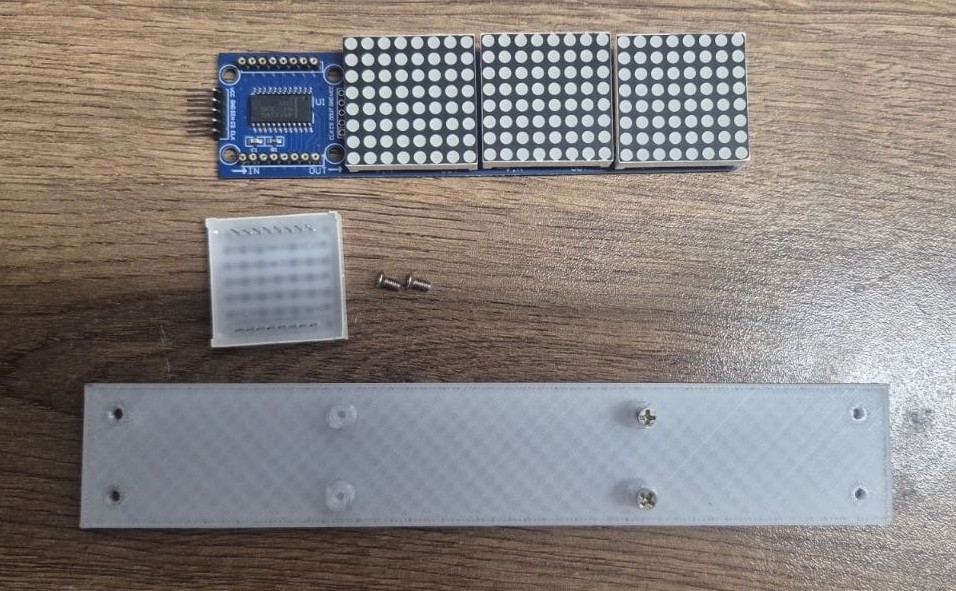
After assembly, I tested the module on the metal frame to verify the dimensional fit and installation accuracy. The test confirmed that all dimensions were correct and the module fit into the intended position without any issues, validating the accuracy of the design and its readiness for final integration.
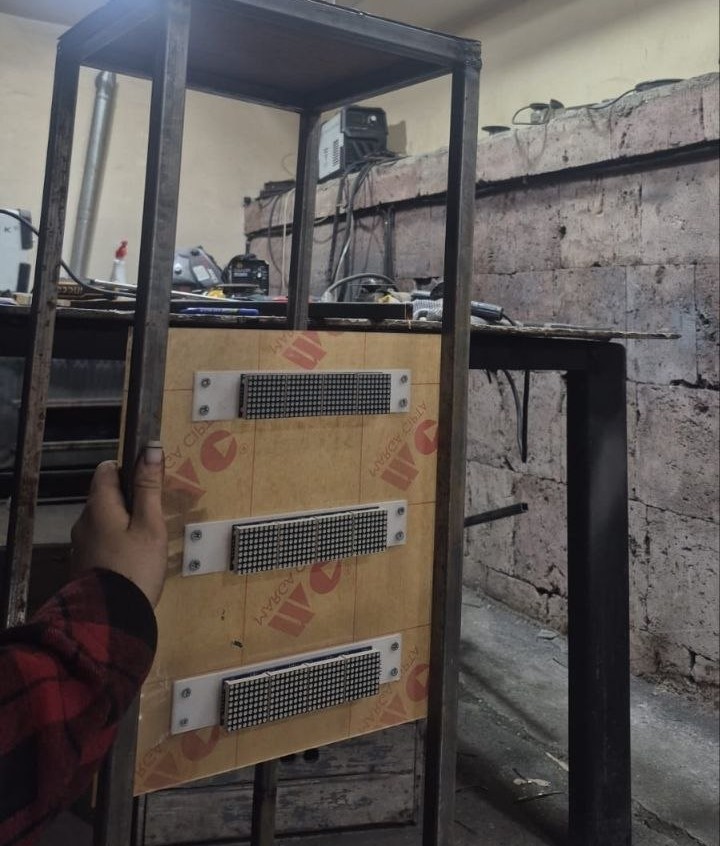
The final installation of the components into the complete metal frame had not yet been completed, as the final version of the frame was still under development. However, all modules were fully prepared and ready for final integration.
Final Packaging and System Integration
At this stage, the prepared mechanical, electronic, and display subsystems were brought together for final packaging and system integration. The main PCB, power supply, voltage regulator, LED displays, sensors, and LED strips were prepared for installation in their designated positions within the overall structure.
The electronic modules were installed in their protective enclosures, while the display module was assembled on the acrylic base. The mounting points and fastening elements designed during the system integration process allow the different components to be securely attached to the main structure using screws, bolts, and nuts.
The wiring was also organised during the final packaging process, ensuring that power and signal connections could be routed safely and in an organised manner between the different modules. The enclosures protect the electronic components, while the mounting structures ensure the stable positioning of the displays and other elements.
At the time of documenting this week, the final metal frame and the complete mirror-based structure were still under development. Therefore, the complete installation of all prepared modules into the final structure had not yet been completed. However, the individual enclosures, display mounting structure, electronic subsystem, and power system had already been designed, fabricated, assembled, and tested, and were ready for final integration.
The remaining work includes completing the final metal structure, integrating the mirror and acrylic display assembly, installing the prepared electronic enclosures and LED lighting, and completing the final packaging and system integration of the project. The complete final result and the final integrated system will be documented and presented on the Final Project page as the project develops.
Conclusion
This week focused on integrating the mechanical, electronic, and structural parts of my final project. I designed and fabricated protective enclosures and mounting structures, prepared the wiring and connectors, and assembled and tested the electronic subsystem.
The main PCB, sensors, displays, LED strips, power supply, voltage regulator, and display mounting system were successfully prepared and tested as functional parts of the project. The different subsystems were also checked for compatibility and prepared for integration into the main structure.
Although the complete final assembly had not yet been finished during this week, the main mechanical and electronic components had been designed, fabricated, assembled, and tested. This provided a solid foundation for completing the remaining mechanical integration and final assembly of the project.