Week 6. Electronics design
Group Assignment
The goal of this week’s group assignment was to use the test equipment available in our lab to observe and analyze the operation of a microcontroller-based circuit board. During the assignment, we explored different measurement tools and learned how they can be used for testing and debugging electronic systems.
Particular attention was given to the use of a logic analyzer. By using it, we were able to observe digital signals, analyze their timing characteristics, and better understand the communication between the microcontroller and other components. This helped us gain practical experience in monitoring and interpreting digital data signals.
This activity improved our understanding of electronic testing and debugging techniques and demonstrated the importance of measurement tools in electronics development. The knowledge gained during this assignment will be useful for future PCB testing and system development tasks.
The complete documentation of the group assignment can be found on the Group Assignment page.
Individual Assignment
Basic Circuit Analysis
Electronics Design individual assignment includes circuit simulation, the purpose of which is to test the circuit’s operation in a software environment in advance, ensuring that all components are connected correctly, the calculations are accurate, and the circuit will function as intended before physical fabrication. During the assignment, Onik Babajanyan explained Ohm’s Law to me, which describes the relationship between voltage, current, and resistance and is one of the fundamental laws for calculating electrical circuits.
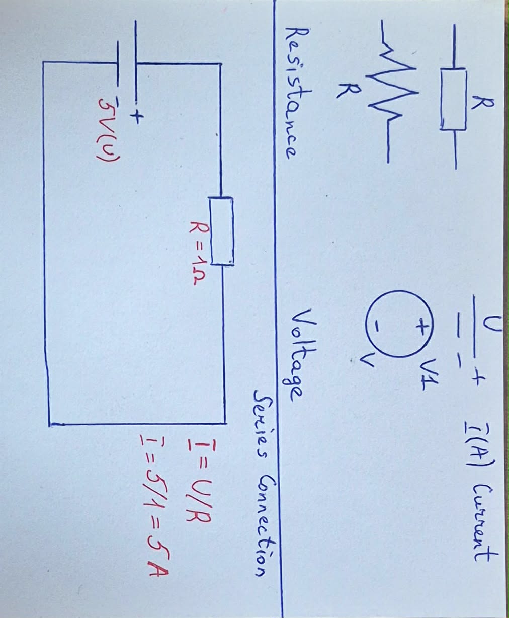
According to Ohm’s Law, current is equal to voltage divided by resistance (I = V / R). To properly understand this relationship, it is important to distinguish the symbols and measurement units: R is resistance and is measured in ohms (Ω), I is current and is measured in amperes (A), and U or V is voltage measured in volts (V). The relationship between these quantities allows calculation of any unknown parameter in a circuit if the other two are known, which is important both for theoretical analysis and for circuit design and simulation.
Circuit Description
The given electrical circuit consists of a 5V voltage source and a single resistor R = 1Ω connected in a closed loop. In the circuit, current flows from the positive terminal of the source through the resistor and returns to the negative terminal. This configuration represents the simplest single-resistor electrical circuit and is used as a classical example to demonstrate the application of Ohm’s Law.
Current Calculation
The current in the circuit is calculated using Ohm’s Law, which states that current equals voltage divided by resistance. For this circuit, the voltage is U = 5V and the resistance is R = 1Ω. Substituting these values into the formula gives I = U / R = 5 / 1 = 5A. Therefore, the current flowing through the circuit is 5 amperes. Using this circuit, we calculated the amount of electric current flowing through the circuit, which represents the charge passing per unit time. Since the circuit contains only one resistor, the entire voltage drops across it, which corresponds to the theoretical principles of simple circuits.
Analysis and Conclusion
The analysis of this circuit shows that current is directly proportional to voltage and inversely proportional to resistance, which fully agrees with Ohm’s Law. Since the resistance value used is small (1Ω), the resulting current in the circuit is large (5A). This confirms that when resistance is small, current increases significantly, and when resistance is large, current decreases.
This simple circuit makes it possible to theoretically understand the relationship between voltage, current, and resistance and serves as a fundamental example for analyzing and designing electronic circuits. Such preliminary calculations are an important stage before simulation and physical implementation, as they help predict circuit behavior and prevent possible errors or component damage.
LTspice Simulation

Image source: LTspice official Facebook page
The circuit was recreated in LTspice to verify its operation through simulation and to confirm the theoretical calculations. A DC voltage source set to 5V was placed, and a 2Ω resistor was connected in series in the circuit. The negative terminal of the source was connected to ground to define the reference node. To run the simulation, a transient analysis command was added with a duration of 1 second. As a result, the current flowing through the circuit was observed to be about 2.5A, which fully matches the theoretical value calculated using Ohm’s law: I = V / R = 5 / 2 = 2.5A.
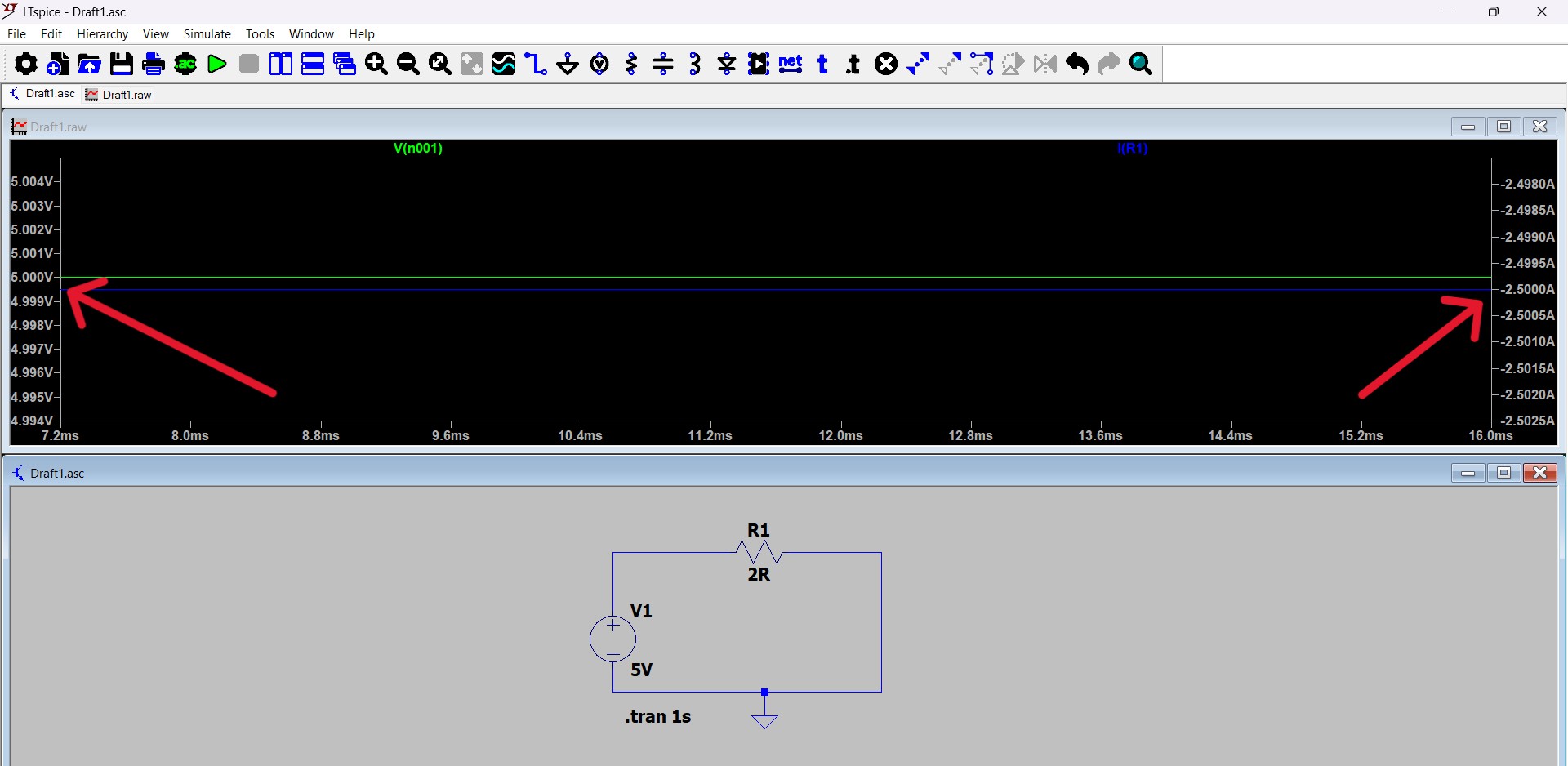
The current value was measured in LTspice using the probe tool by clicking on the corresponding component, which displayed both the graph and the precise numerical value.
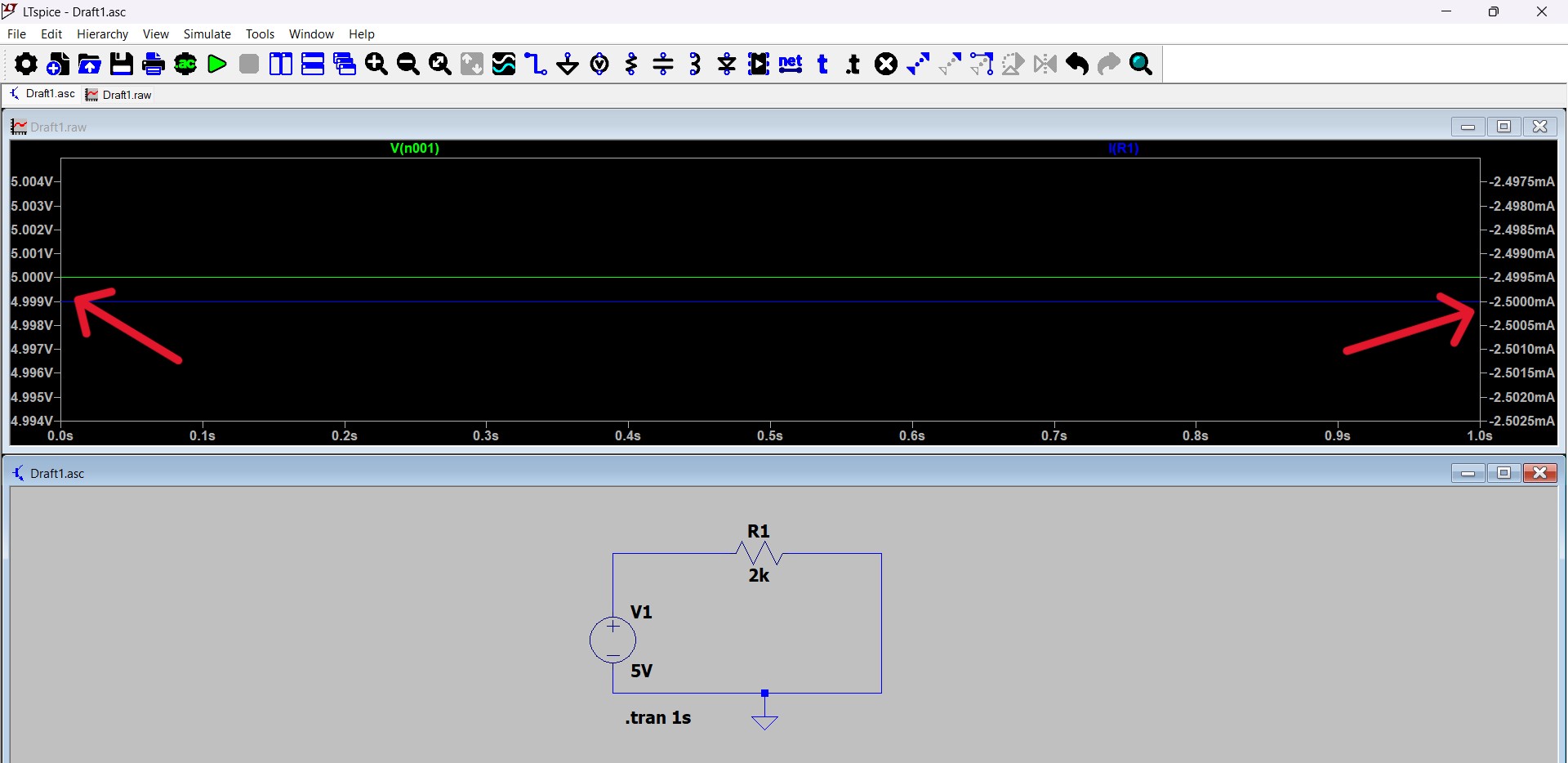
In the second experiment, the resistance value was changed to 2kΩ. In this case, the current became 2.5mA, meaning it decreased by a factor of 1000, because the resistance became 2000Ω instead of the previous 2Ω. This also agrees with Ohm’s law: I = 5V / 2000Ω = 0.0025A = 2.5mA.
In the third experiment, the circuit was modified to form a voltage divider circuit. In this case, two resistors were connected in series: R₁ = 2kΩ and R₂ = 2kΩ, while the voltage source remained the same at 5V. In a series connection, the total resistance equals the sum of the resistances: R_total = R₁ + R₂ = 2000Ω + 2000Ω = 4000Ω.
According to Ohm’s law, the current flowing through the circuit is: I = V / R = 5 / 4000 = 0.00125A = 1.25mA.
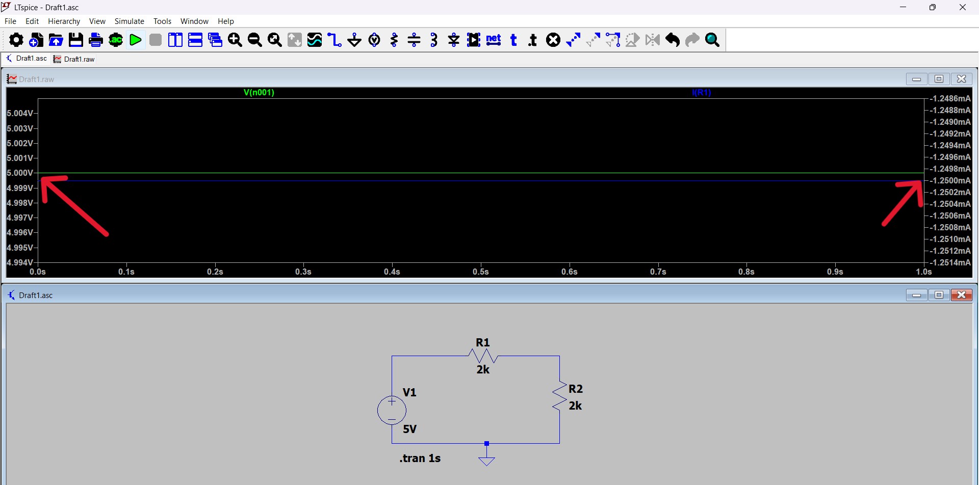
From the simulation graph, a current of about 1.25mA was observed, which fully matches the theoretical calculation. Since the resistors are equal, the voltage is divided equally, meaning each resistor has about 2.5V across it. This confirms the operating principle of the voltage divider and shows that the simulation results match the theoretical model.
The voltage divider circuit is used when it is necessary to reduce a higher voltage to a level that is safe for a device. For example, if we have a board that operates at a maximum voltage of 3.3V (such as a Xiao RP2040 microcontroller module), and we connect it directly to a 12V battery, the device may be damaged because it would receive a voltage higher than its allowed limit. In such a case, a voltage divider is used to divide and reduce the input 12V so that the output becomes a safe level, for example around 3.3V. This helps protect electronic components and ensures their correct operation.
Voltage Divider
This section presents the application of a voltage divider circuit whose purpose is to reduce a high input voltage and make it safe for a microcontroller input. The corresponding calculations are provided, and it is explained how the resulting voltage values can be used to monitor the condition of a power source, such as the charge level of a battery.
We have a 12V battery, and it is necessary to monitor whether it is properly charged. To do this, the voltage must be supplied to a microcontroller so it can measure the battery voltage. When fully charged, the battery provides about 12.5V, and when the charge decreases, it may drop to around 11.5V. However, a microcontroller input pin can typically tolerate only about 3.3V maximum, so this voltage cannot be connected directly, as it could damage the device. To solve this problem, a voltage divider circuit is used. For example, let us choose the upper resistor as R₁ = 20kΩ. We must select the second resistor so that when the input voltage is 12.5V, the output becomes about 3.3V. The voltage divider formula is:
Vout = Vin * R2 / (R1 + R2)
The divider circuit was calculated in order to reduce a high input voltage and obtain a safe output voltage for the microcontroller. The supply source was Vin = 12V, and two series resistors were chosen: R₁ = 20kΩ and R₂ = 2kΩ. The lower node of the circuit was connected to GND as the reference node.
First, the current flowing through the circuit was calculated:
I = Vin / (R1 + R2)= 12 / (20000 + 2000)= 12 / 22000
Next, the output voltage across the second resistor was calculated:
Vout = I * R2
or directly using the divider formula:
Vout = Vin * R2 / (R1 + R2)= (12 * 2000) / 22000= 1.09 V
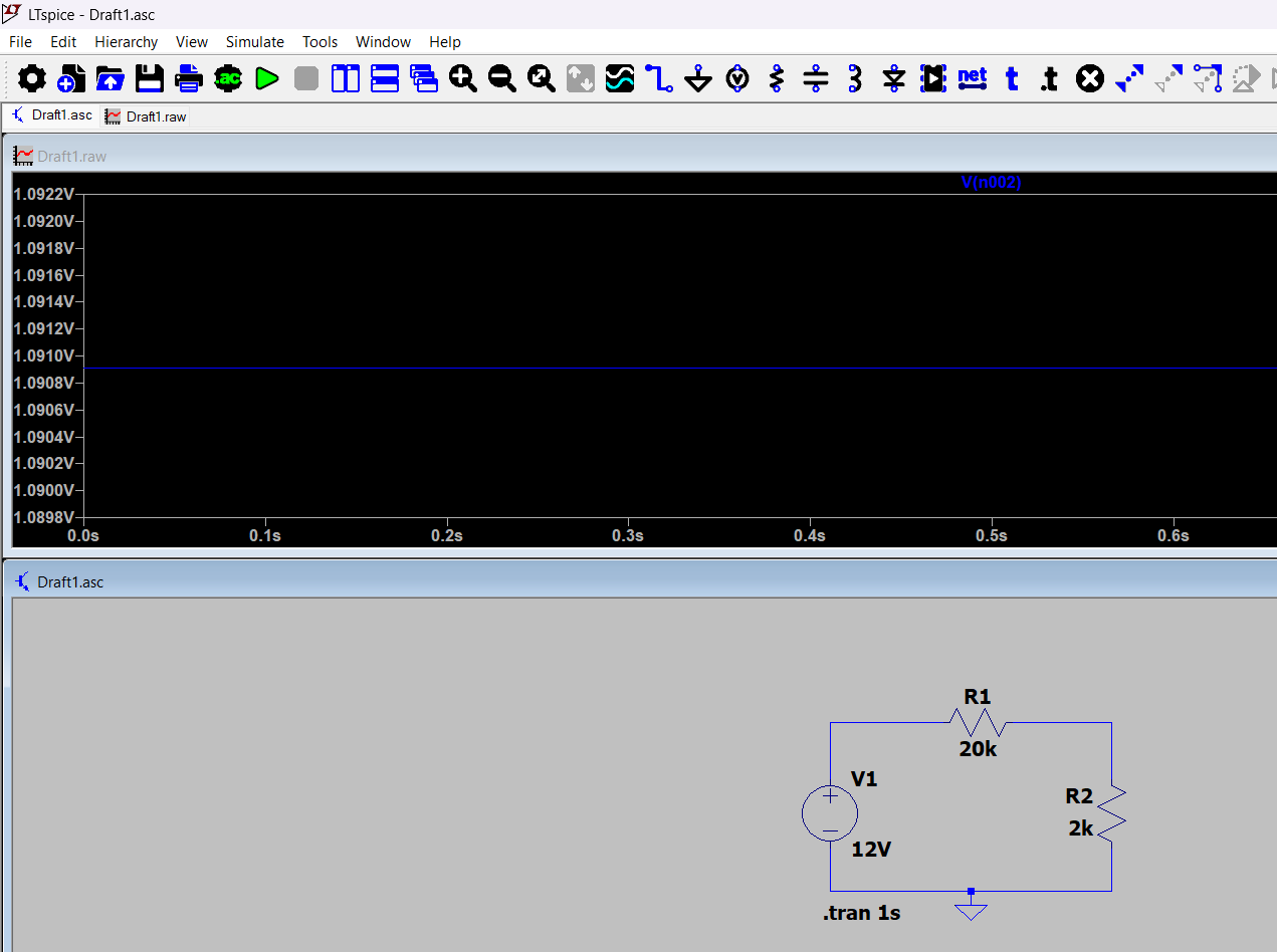
The result is approximately 1.09V, which is significantly lower than 3.3V and therefore safe for a microcontroller input. This confirms that the selected resistor ratio is appropriate for reducing high voltage for measurement or sensing purposes.
If the measured voltage at the microcontroller input pin is approximately 1.09V, this indicates that the source voltage at the divider input is about 12V, meaning the battery is fully charged (around 100%). This matches the calculation, since with the chosen resistor ratio a 12V input is divided to about 1.09V.
If the battery voltage decreases during operation and becomes 11V instead of 12V, the divider output voltage will also decrease. According to the calculation:
Vout = Vin * R2 / (R1 + R2) = 11 * (2 / 22) = 1 V
Thus, if the microcontroller input pin measures about 1V (instead of 1.09V), a condition can be defined in software indicating that the battery is in a discharged state, for example around 20% charge. In this way, the microcontroller can monitor battery status simply by measuring the divider output and comparing it to predefined threshold values.
If we change the input voltage to 11V and use a divider with R₁ = 20kΩ and R₂ = 5kΩ, then according to the formula:
Vout = Vin * R2 / (R1 + R2)
we obtain:
Vout = 11 * (5 / (20 + 5))=11 * (5 / 25)=2.2 V
This means that if the microcontroller input pin reads about 2.2V, the program can interpret this as a drop in battery voltage. In that case, the microcontroller can respond—for example, by generating a sound alert, turning on a red LED indicator, or sending a warning signal. This approach allows automatic monitoring of battery status and timely notification when the charge decreases.
Capacitors
Capacitor in Electronic Circuits
A capacitor is one of the fundamental components used in electronic circuits. Its main function is to store electrical energy temporarily in the form of an electric field. A capacitor consists of two conductive plates separated by an insulating material called a dielectric. When voltage is applied across the plates, electric charge accumulates on them, allowing the capacitor to store energy.
The ability of a capacitor to store charge is called capacitance and is measured in farads (F). In practical electronics, smaller units such as microfarads (µF), nanofarads (nF), and picofarads (pF) are more commonly used.
The basic relationship that describes a capacitor is:
Q = C × V
where Q is the stored charge (coulombs), C is the capacitance (farads), and V is the voltage across the capacitor (volts).
Capacitors are widely used in electronic circuits for several purposes. One common application is filtering and smoothing voltage in power supply circuits. When a capacitor is connected across a power supply line, it can store energy and release it when the voltage temporarily drops, helping stabilize the voltage level.
Another important use of capacitors is decoupling or bypassing in microcontroller circuits. In such cases, a small capacitor (for example 0.1µF) is placed between the power supply (VCC) and ground (GND) close to the microcontroller. This helps remove noise and sudden voltage fluctuations that may affect the operation of the microcontroller.
Capacitors are also used in timing circuits, signal filtering, and energy storage applications. Because they can charge and discharge over time, they are often combined with resistors to form RC circuits that control timing behavior in electronic systems.
Understanding the behavior of capacitors is important when designing electronic circuits, especially when working with microcontrollers and sensors, because they help improve stability, reduce noise, and protect sensitive components.
Capacitor in a Parallel Circuit
The diagram below shows a simple electronic circuit that includes a capacitor. On the left side of the circuit there is a 12V battery, which acts as the power supply. To the right of the battery a capacitor is connected, and further to the right there can be a load, for example a motor or a small lamp/LED.
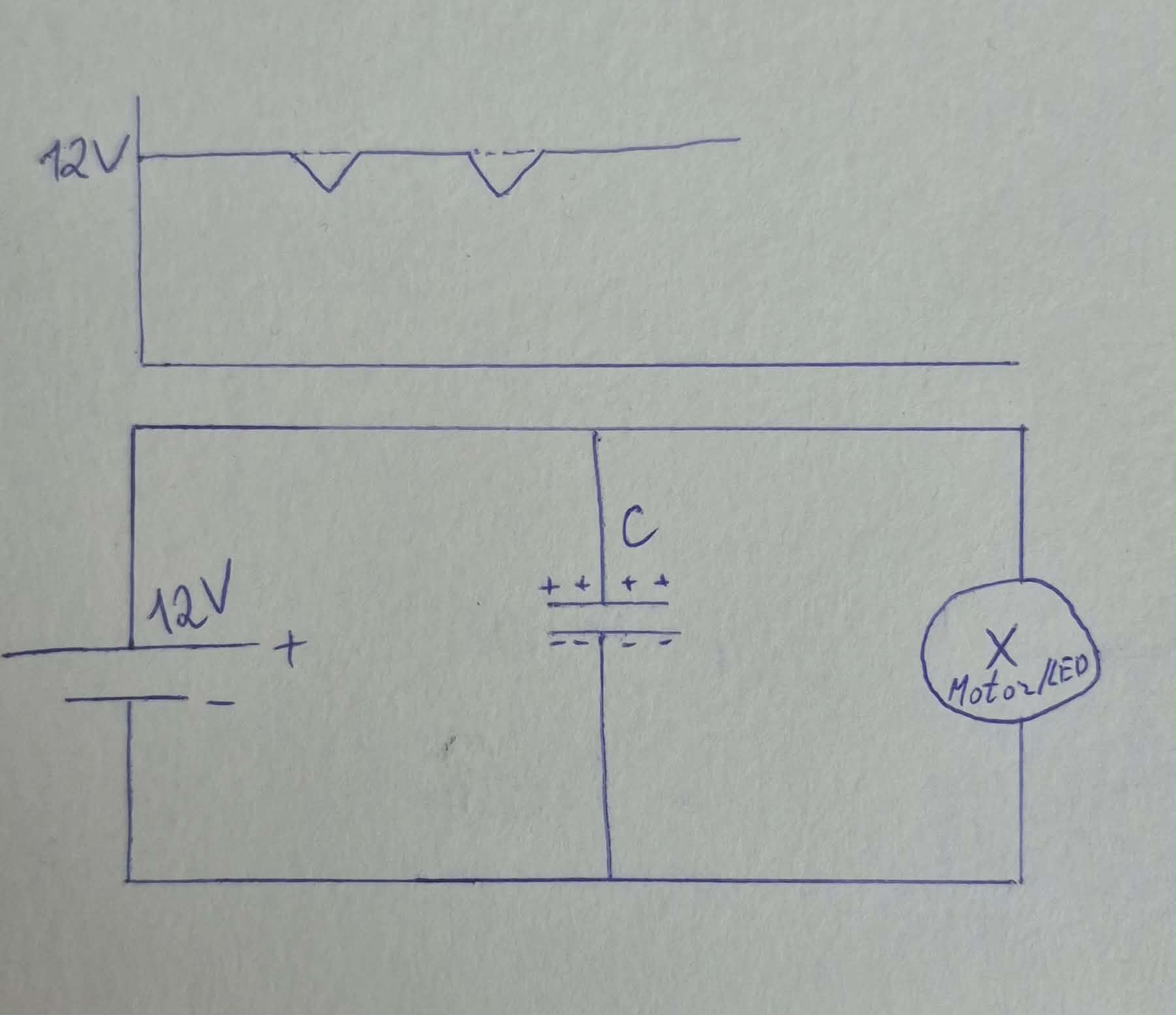
In this circuit the capacitor is connected in parallel with the power supply. When the circuit is powered, current does not continuously flow through the capacitor as it does through a resistor. Instead, the capacitor stores electrical energy between its plates.
The ability of a capacitor to store energy is called capacitance (C). When voltage is applied across the capacitor, an electric field is created between its two conductive plates. During this process positive charges accumulate on one plate, while negative charges accumulate on the other plate. From physics we know that opposite charges attract each other, and this attraction forms the electric field where the energy is stored.
In this configuration the capacitor acts as a temporary energy storage element. While the circuit is operating, the capacitor charges and stores energy. If later a device is connected to the circuit or if there is a voltage fluctuation or drop, the capacitor can discharge and help compensate for the voltage drop, keeping the circuit more stable.
For this reason, capacitors are widely used in electronic circuits for voltage stabilization, noise reduction, and temporary energy storage.
Power Supply Noise and Capacitor Filtering
In real electronic systems, a power source is never ideal. Every battery or power supply has a small internal resistance called parasitic resistance. In this simulation the 12V battery is modeled with a very small internal resistance of 0.1Ω. Additionally, a small AC signal of 0.4V is added to represent noise or ripple that can appear in real power supplies.
No Capacitor (First Simulation)
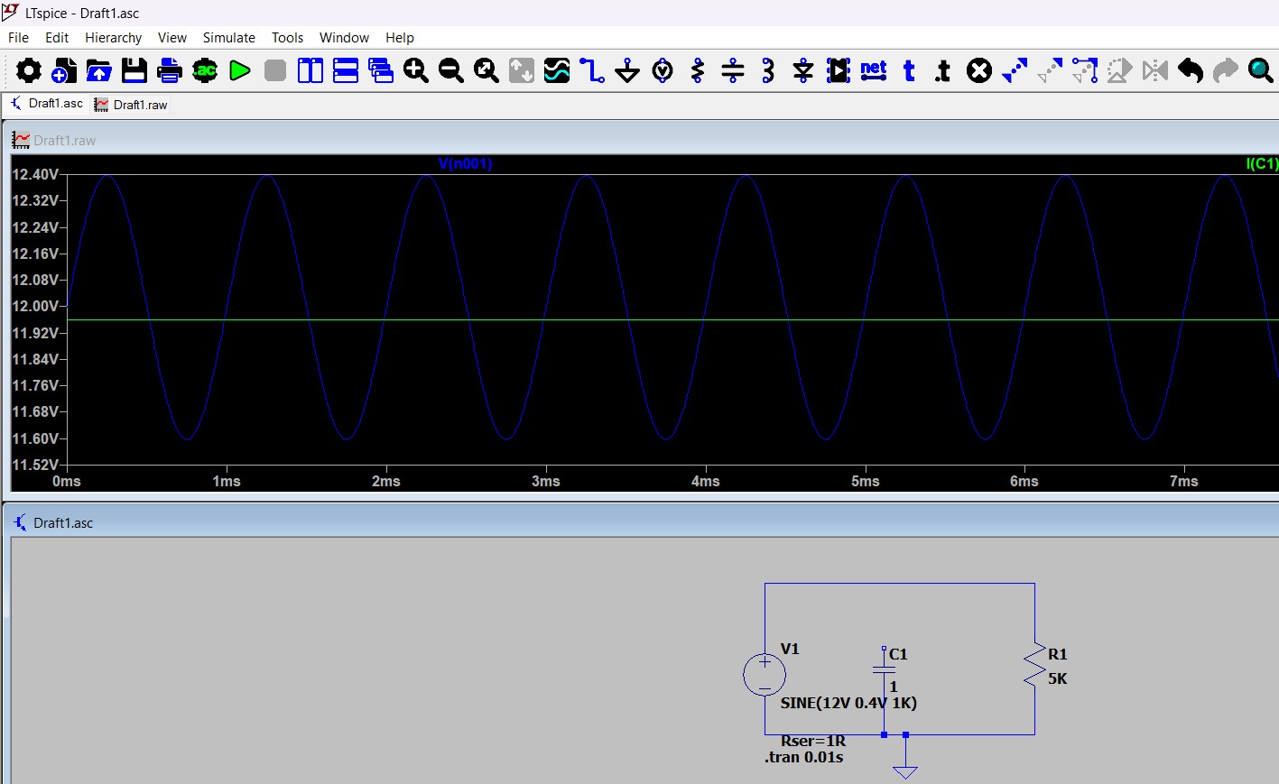
In the first simulation the circuit includes a 12V power source with a small AC component and a 5kΩ resistor load. Because the source contains a small AC signal, the output voltage is not perfectly stable.
From the graph we can see voltage oscillations around 12V. This means that the voltage is slightly increasing and decreasing over time. In electronic systems this behavior is called power supply noise or ripple.
Such oscillations can be dangerous for electronic devices, especially for sensitive circuits such as microcontrollers, sensors, or computers. A stable power supply is very important for reliable operation.
In real life, the electricity in our homes is AC power, which varies sinusoidally between positive and negative values (for example about −220V to +220V in many regions). When we connect devices like a laptop charger, the charger converts this AC voltage into a stable DC voltage, for example 12V or 19V, using rectification and filtering circuits.
If this conversion and filtering is not done correctly, the output voltage may contain large fluctuations, which can damage electronic devices such as laptops or embedded systems.
Capacitor Filtering (Second Simulation)
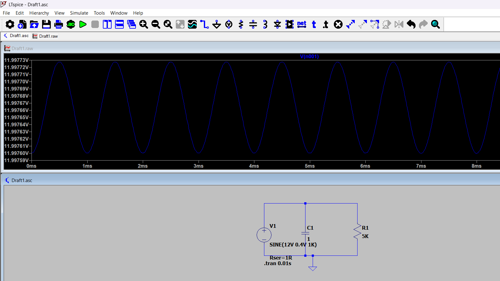
In the second simulation a capacitor is connected in parallel with the power supply and the load. The capacitor acts as a filter for the power supply.
When the voltage slightly increases, the capacitor stores energy by charging. When the voltage drops, the capacitor releases energy by discharging. Because of this behavior, the capacitor helps smooth the voltage.
As we can see in the second graph, the voltage oscillations become much smaller, and the output voltage becomes almost a straight line near 12V. This means the power supply is now much more stable.
For this reason, capacitors are widely used in electronic circuits as decoupling or filtering capacitors, helping reduce noise and stabilize the power supply voltage.
Designing the PCB in KiCad

Source: CADLAB.io – Visual version control for KiCad
This week I designed the electronics for my Final Project using KiCad. The workflow included installing the Fab Library, creating the schematic, assigning footprints, designing the PCB layout, and verifying the design using ERC and DRC.
Fab Library Installation
Before starting the schematic design, I installed the Fab Library in KiCad using the Plugin and Content Manager. To do this, I opened the Plugin and Content Manager from the KiCad menu, searched for the Fab Academy Library, and installed it. After the installation was completed, I restarted KiCad so that the new library would be loaded correctly.
The Fab Library contains the symbols and footprints commonly used in Fab Academy projects, making both schematic capture and PCB design much easier. After restarting KiCad, I verified that the library had been installed successfully by opening the Schematic Editor and checking that the Fab Academy components were available through the Add Symbol tool. The same components also became available in the PCB Editor for footprint assignment.

Creating the Schematic
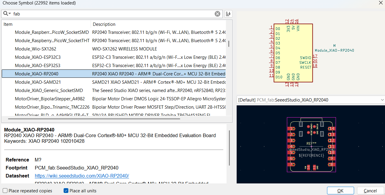
After installing the Fab Library, I opened the Schematic Editor and started creating the electronic schematic for my Final Project. First, I added all the components required for the design. Using the Add Symbol tool, I selected the necessary components from the Fab Library, including the Seeed Studio XIAO RP2040 microcontroller, the voltage regulator, resistors, capacitors, MOSFET, connectors, and the other electronic components used in the project.
Connecting Components and Using Net Labels
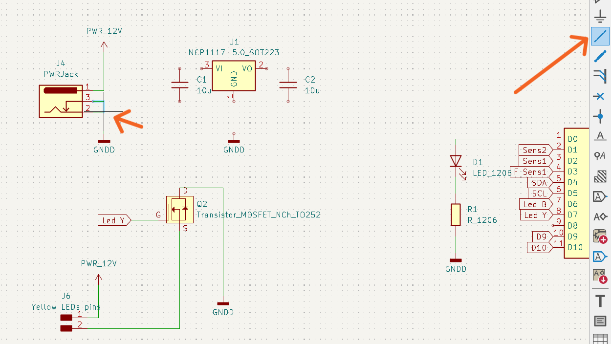
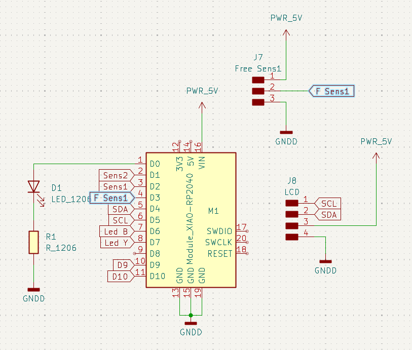
After placing all the components, I connected them using electrical wires. To keep the schematic clean and easy to read, I used Net Labels instead of drawing long wires across the schematic. I assigned meaningful names to the important nets, such as 12V, 5V, GND, SDA, SCL, and the signal lines for the sensors. This approach made the schematic much more organized and simplified future editing.
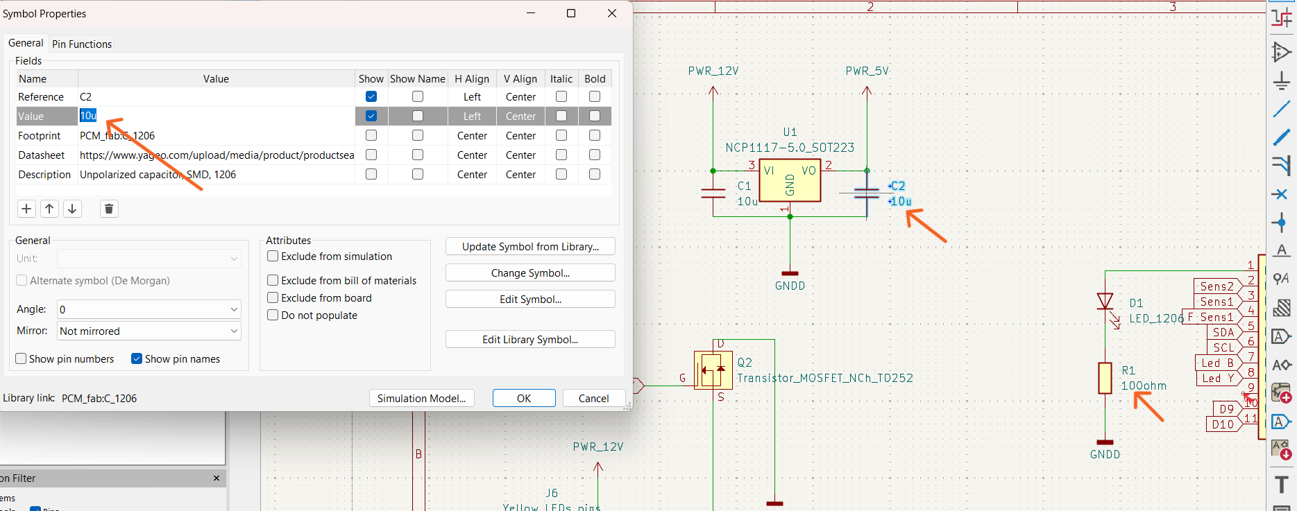
Assigning Component Values
Once all the components were connected, I assigned the appropriate values and designations to each one.
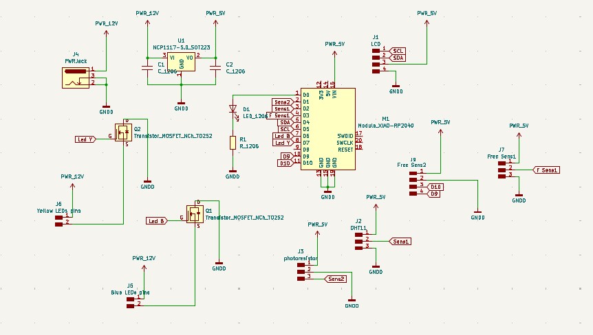
I specified the resistance values for resistors, the capacitance values for capacitors, and the correct part names for the voltage regulator, connectors, and the remaining components. This step was important to ensure that every component could be correctly identified during the PCB design process.
Electrical Rules Check (ERC)
After completing the schematic, I ran the Electrical Rules Check (ERC) to verify all electrical connections.
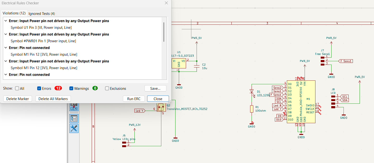
The ERC reported a few messages, mainly related to pins that were intentionally left unused in this project. For example, the 3.3V power pin was not required because the system operates from a 5V supply, and several unused GPIO pins were intentionally left unconnected. Since these pins were not needed for the intended functionality, the reported messages did not affect the operation of the circuit. After reviewing the ERC results, I confirmed that all essential connections were correct and that the schematic was ready for the next stage of the design process: PCB layout.
Main Electronic Components
As the main controller of the system, I used the Seeed Studio XIAO RP2040 microcontroller module. This board is compact, has enough input/output pins, and supports several communication protocols such as I2C, which is useful for connecting the LCD display.
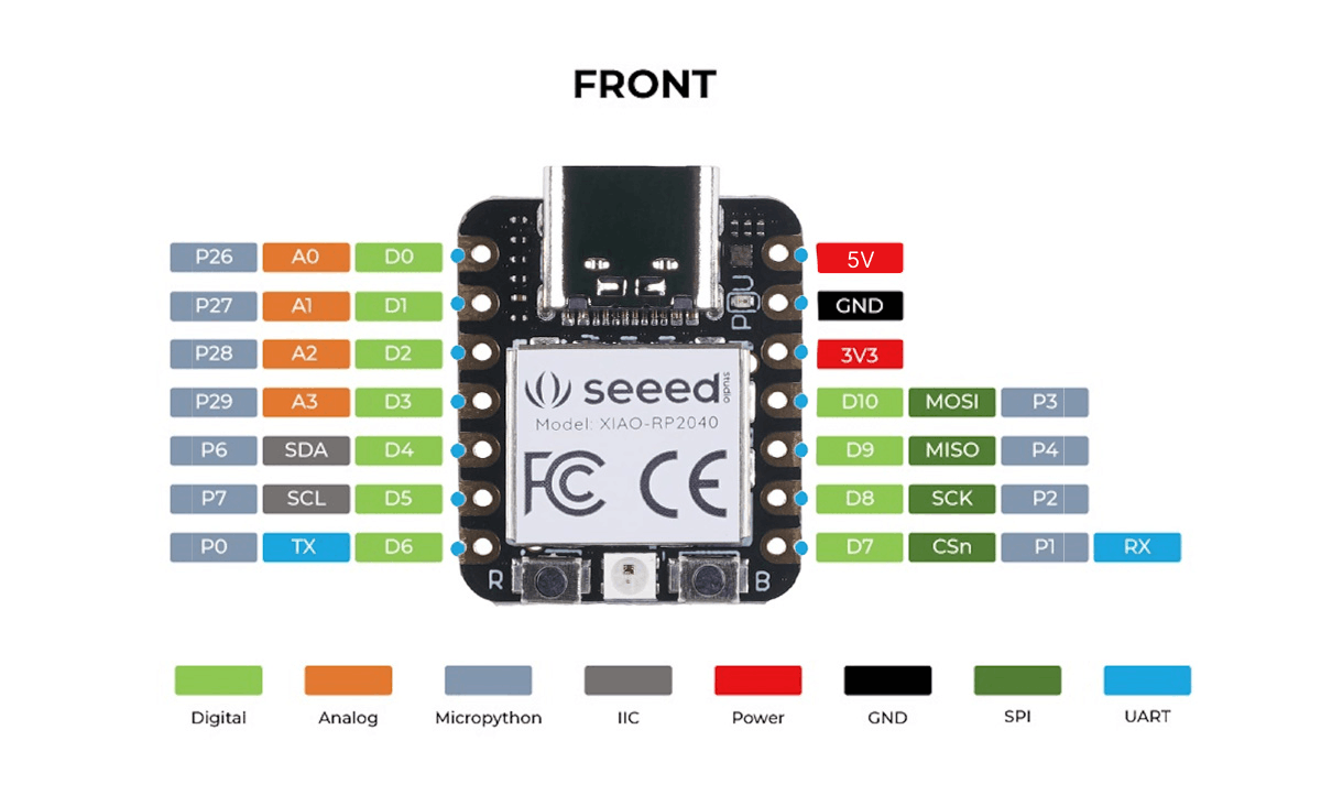
Image source: Zephyr Project Documentation, XIAO RP2040 Board Documentation.
While designing the power system, I planned for the entire board to be powered by a 12V adapter.
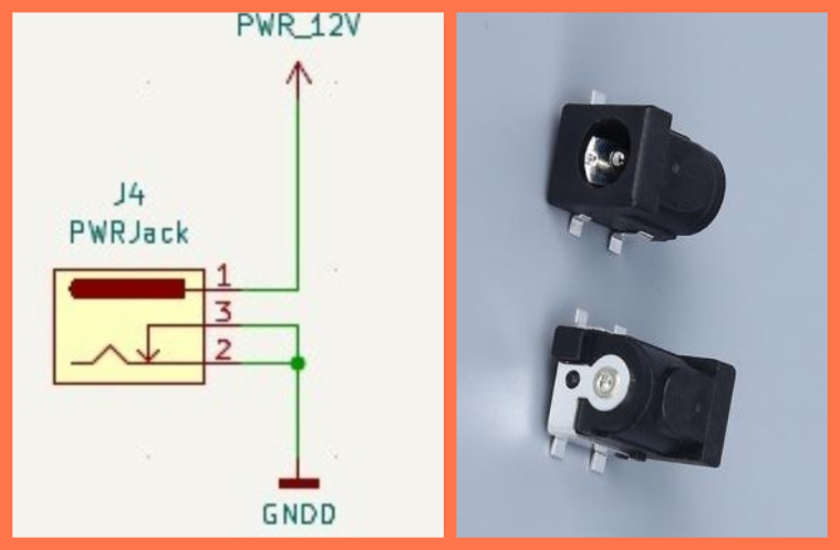
Source: KLS Electronic. SMT DC Power Jack Connector (Model 2525)
The 12V power enters the board through a power jack connector. Since the microcontroller and some sensors require 5V to operate, voltage regulation was necessary. For this purpose, I used the NC1117 Voltage Regulator, which converts the 12V input voltage into a stable 5V output voltage. Capacitors were added at the input and output of the regulator to stabilize the voltage and reduce electrical noise.
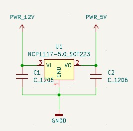
Source: Robu.in – NCP1117ST33T3G 3.3V 1A LDO Regulator
After completing the power circuit, I connected the sensors and the other components.
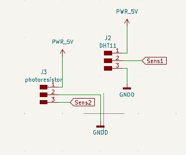
To measure the ambient light level, I used a Photoresistor (LDR).
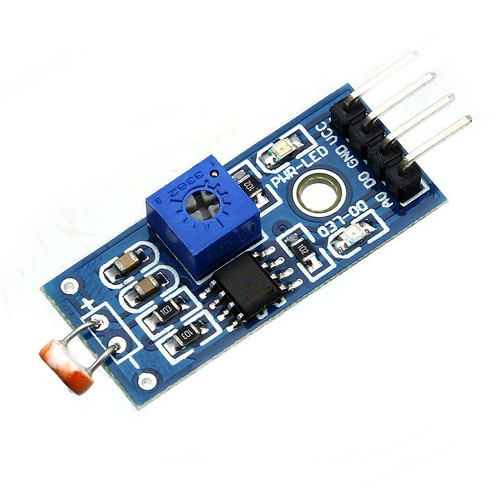
A photoresistor changes its resistance depending on the intensity of the light falling on it. This sensor is connected to the microcontroller so that the system can read changes in light levels and decide when to turn the LED lighting on or off.
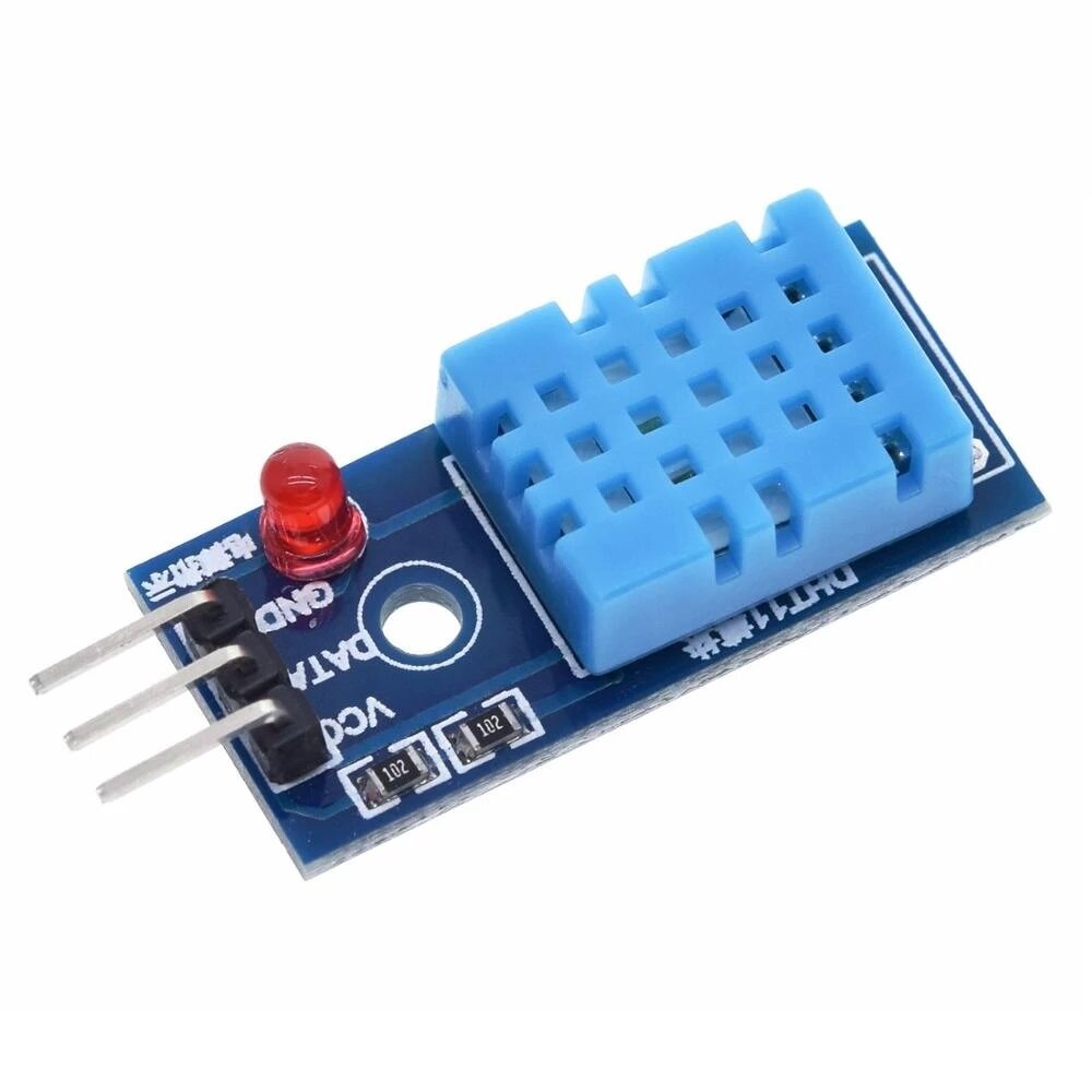
To measure environmental conditions, I used the DHT11 sensor.

Source: OSEPP, DHT11 Datasheet, p. 5. Retrieved from ALLDATASHEET
This sensor provides digital data about the surrounding temperature and humidity. It is connected to a digital pin of the microcontroller and powered with 5V.
To display the collected data to the user, I used an I2C LCD Display.
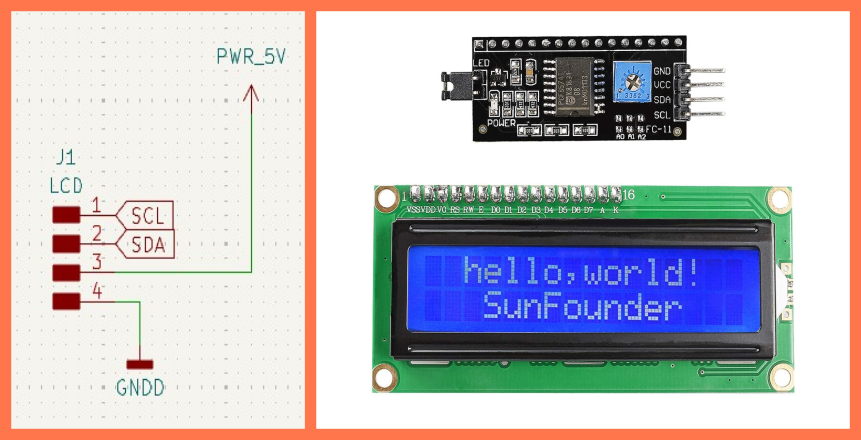
Source: SunFounder IIC/I2C/TWI LCD1602 Display Module. Image retrieved from Amazon
The LCD display is connected to the microcontroller using the I2C communication protocol, which requires only two wires: SDA and SCL. This approach saves microcontroller pins and simplifies the connections.
The system also includes 12V LED strip lights that will be used for lighting control.
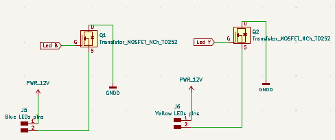
Since the microcontroller pins cannot directly control high-voltage loads, the LED strips are controlled using MOSFET transistors.
The MOSFETs act as electronic switches: the microcontroller sends a small control signal to the gate, allowing the transistor to safely turn the 12V LED strip on or off.
After finishing the schematic design, the next step was assigning footprints to all the components. The footprint defines how each component should be physically placed and soldered onto the PCB.
After assigning the footprints, I moved to the PCB design stage in KiCad. During this stage, I placed the components in a way that kept the connections as short and organized as possible. Proper component placement is important because it simplifies routing and improves the overall reliability of the circuit.
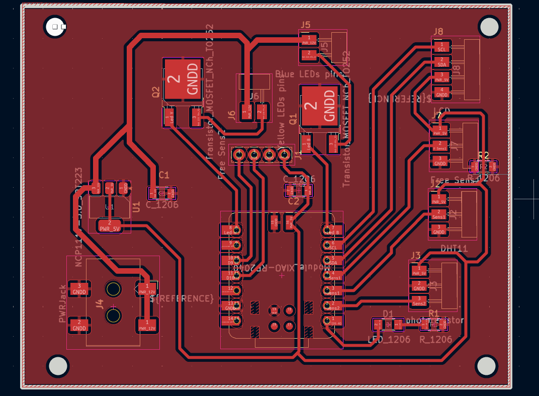
After positioning the components, I routed all the electrical traces between them. I tried to keep them as short and organized as possible while avoiding unnecessary crossings. During the PCB design, a full ground plane was used, which helps reduce electrical noise and improve the overall stability of the system. In addition, the Edge Cuts layer was added to define the board outline and cutting boundaries. Mounting holes with a diameter of 3.2 mm were also included so that the board can be securely fixed to a surface or structure in the future.
During the design process, I also considered the possibility of expanding the system in the future. For this reason, I left several free sensor pins on the microcontroller that can later be used to connect additional sensors.
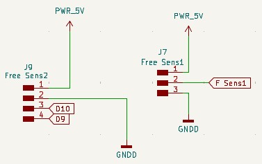
These pins are brought out to connectors, which will make it easier to add new modules without redesigning the entire board. This approach makes the system more flexible and modular, allowing future integration of additional sensors such as motion sensors, gas sensors, or other environmental monitoring devices.
PCB Design
After assigning the footprints to all the components, I switched to the PCB Editor to design the board layout. The PCB design process included configuring the board rules, routing the electrical traces, adjusting the component labels, defining the board outline, and verifying the design using the Design Rule Check (DRC).
Board Setup (Design Rules)
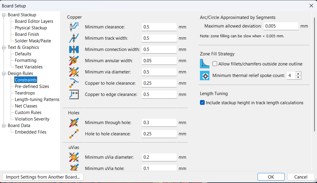
Before starting the PCB routing, I configured the Board Setup by defining the required Design Rules. In the Constraints tab, I specified the minimum track width, minimum clearance between tracks, and the minimum via and hole sizes according to the manufacturing requirements. These settings helped ensure that the PCB could be manufactured correctly and reduced the likelihood of design rule violations during the DRC process.
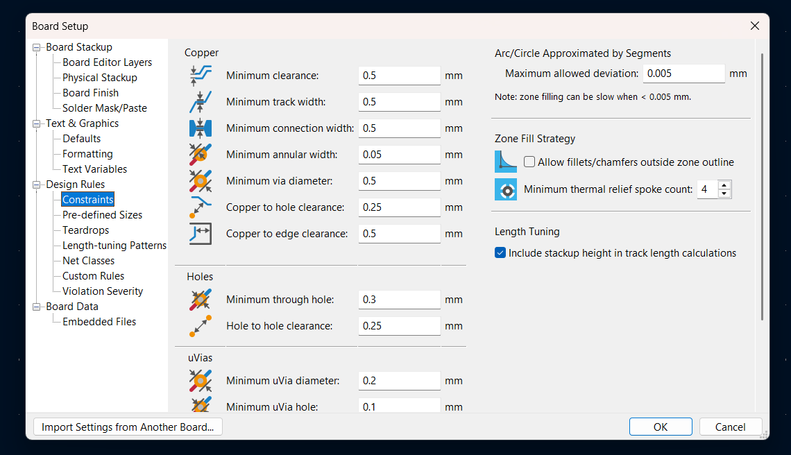
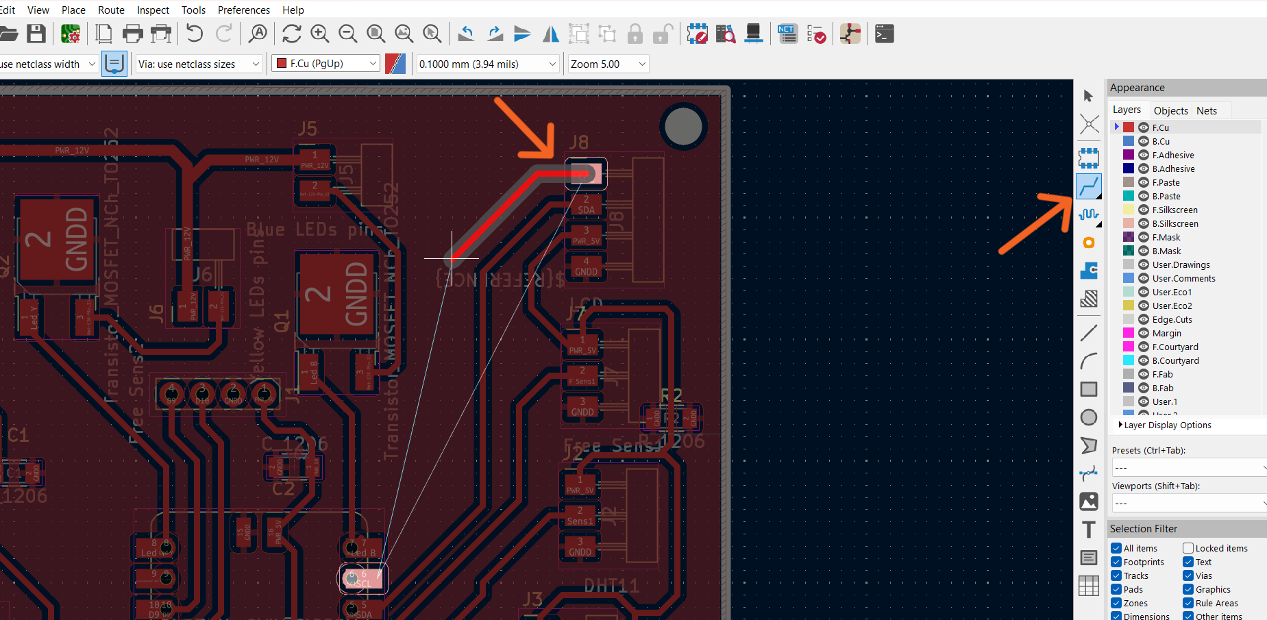
Tracing the Tracks
After configuring the board settings, I started routing the PCB traces using the Route Tracks tool. I connected all the pads that belonged to the same electrical net while keeping the traces as short and organized as possible. I also followed the design rules defined in the Board Setup to maintain the required clearances and track widths. In addition, I used a ground plane to reduce electrical noise and improve the overall stability of the circuit.
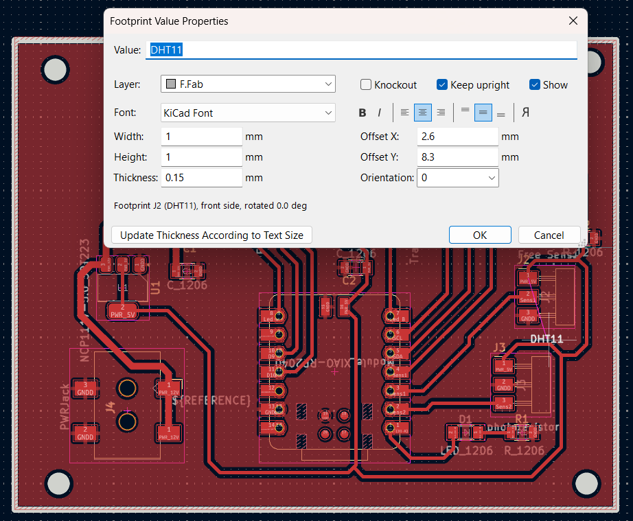
Adding Component Names
After completing the routing, I adjusted the component names (Value) on the PCB. Using the Footprint Value Properties window, I modified the position, size, and visibility of the labels to ensure that they were clearly readable and did not overlap with other PCB elements. This makes the board easier to assemble and inspect.
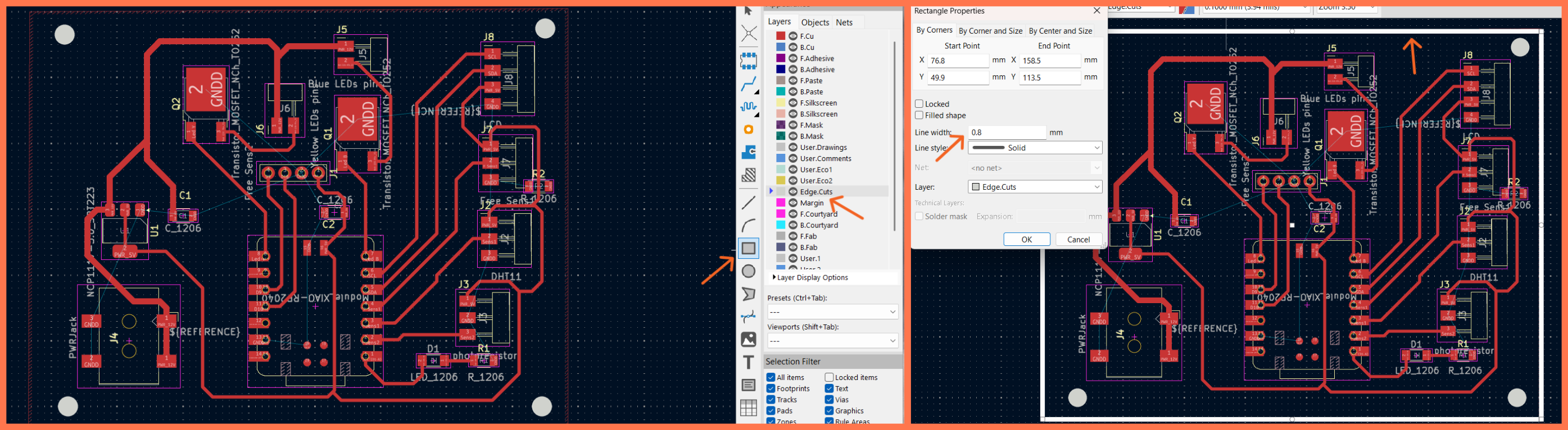
Adding Edge Cuts
As one of the final steps of the PCB design, I drew the board outline using the Edge.Cuts layer. This layer defines the final shape and dimensions of the PCB and specifies the cutting boundary used during manufacturing. The outline was designed to accommodate all the components while maintaining the intended board dimensions.
KiCad DRC Analysis
After completing the PCB layout in KiCad, a Design Rule Check (DRC) was performed to identify potential design errors before manufacturing.
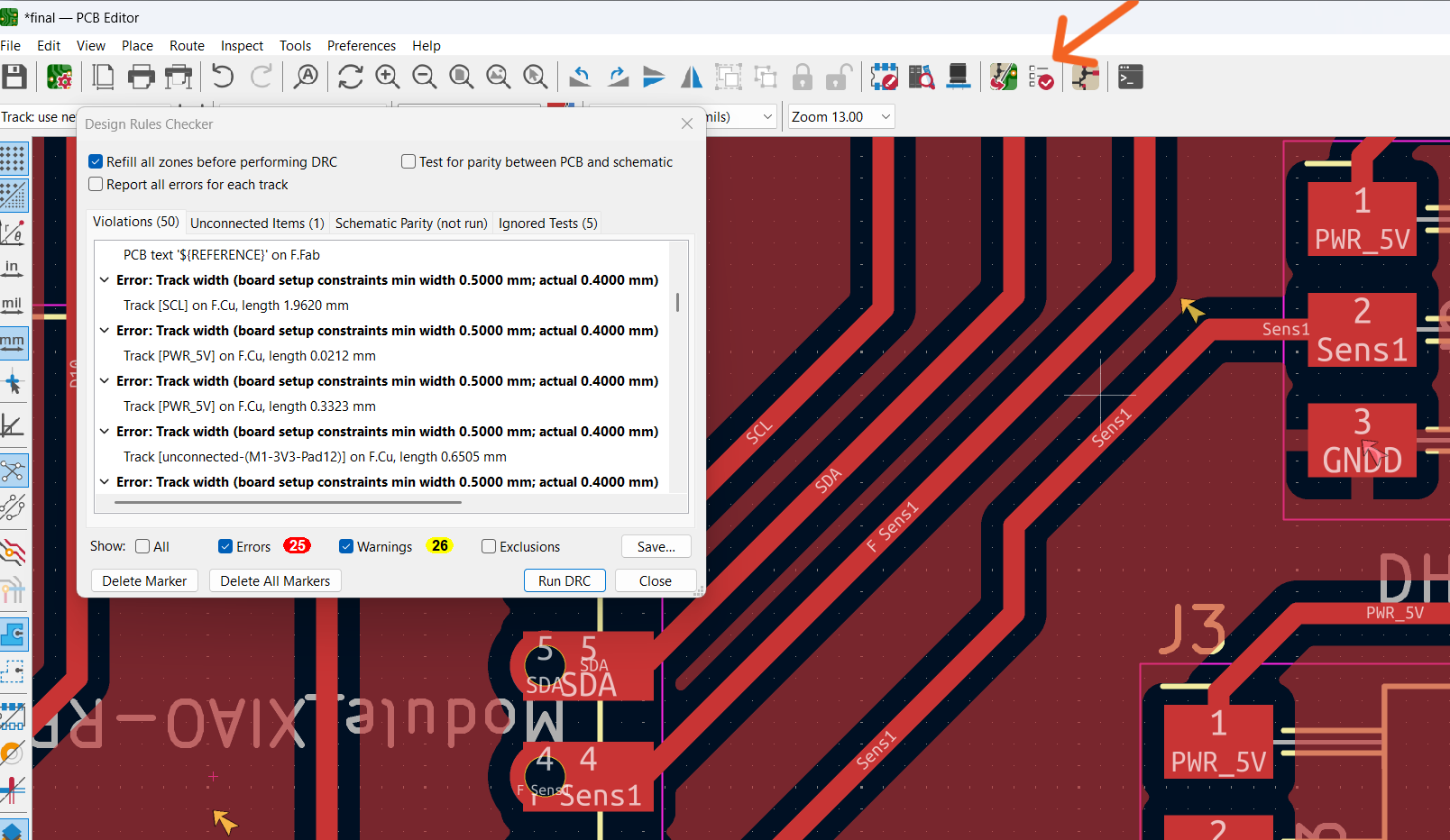
During the first DRC run, several errors and warnings were detected, mainly related to violations of minimum clearance between traces and some incorrect connections. In particular, the system indicated that the defined 0.5 mm minimum clearance was not respected in some areas, meaning that certain tracks were placed too close to each other.
In addition, some unconnected or partially connected nets were also identified, which could lead to incorrect operation or short circuits.
Based on the DRC results, the PCB layout was revised by adjusting routing paths, increasing distances between traces, and fixing the problematic connections. After these modifications, the DRC was run again, and no errors were detected, confirming that the design met the manufacturing requirements.
This iterative verification process played an important role in improving the reliability of the design and preventing potential manufacturing issues, ensuring that all connections and clearances comply with KiCad design rules.
This iterative verification process played an important role in improving the reliability of the design and preventing potential manufacturing issues, ensuring that all connections and clearances comply with KiCad design rules.
Final PCB Layout
The final PCB layout includes the microcontroller, voltage regulator, sensors, LCD display, MOSFET drivers, power input, LED strip connections, and mounting holes. After completing the routing, defining the board outline, and resolving all DRC issues, the board was ready for manufacturing and assembly.
3D PCB View
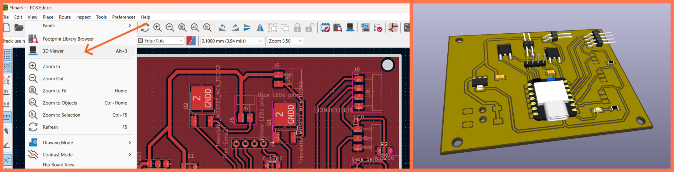
After completing the PCB layout, I used KiCad’s built-in 3D Viewer to inspect the board in three dimensions. This allowed me to verify the placement and orientation of the components, evaluate the overall appearance of the PCB, and confirm that the design was ready for manufacturing. Some components are not visible in the 3D view because their corresponding 3D models are not available in the KiCad library. However, their footprints and electrical connections are correctly included in the PCB design.
Conclusion
This week gave me a complete understanding of the electronics design workflow, from basic circuit analysis to creating a manufacturable PCB.
I began by studying the fundamental principles of electronics, including Ohm’s Law, voltage dividers, and the role of capacitors in filtering and voltage stabilization. By performing simulations in LTspice, I compared theoretical calculations with simulation results and gained a better understanding of circuit behavior before physical implementation.
I then designed the electronics for my Final Project in KiCad. This process included installing the Fab Library, creating the schematic, assigning footprints, performing ERC checks, designing the PCB layout, routing the traces, defining the board outline, and verifying the design with DRC. After resolving all design rule issues, I completed a PCB that is ready for manufacturing and assembly.
Overall, this assignment helped me understand the complete electronics design workflow, from theory and simulation to schematic design and PCB layout. The PCB developed during this week will be used as the main controller board for my Final Project.