Electronics Production
Group assignment
Here is a link to the group assignment page, where my group and I documented the characterization of the design rules for your in-house PCB production process
Individual Assignments:
Electronic production is the manufacturing of electronics. There are several processes to build PCBs, such as etching (acid), milling, and copper cutting. There are also different types of PCBs, including FR1, FR2, and FR4 (which is the one we have at the lab).
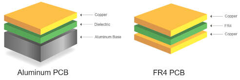
The term "FR4" stands for "Flame Retardant 4," indicating that it meets certain fire resistance standards. FR4 is known for its high dielectric strength, which makes it an excellent insulator. It also provides good dimensional stability and resistance to moisture absorption. FR4 is composed of woven fiberglass cloth saturated with an epoxy resin binder. However, its composition (the fiberglass) is hazardous to mill without the proper precautions. The primary concern when milling FR4 is exposure to fiberglass dust, which can irritate the skin, eyes, and respiratory system if inhaled.
But we take precautions to prevent this.- The machines we have at the lab are closed off.
- We use dust collection systems or vacuum attachments on milling equipment to minimize airborne dust.
- Other precautions could also be used, such as using gloves and masks.
- During the global open time zoom call, it was also mentioned that applying a small coat of oil on the board would trap the fiberglass dust and prevent it from becoming airborne. However, I have not tried this yet as it depends on the type of oil used, as some could attack the copper.
Design Process
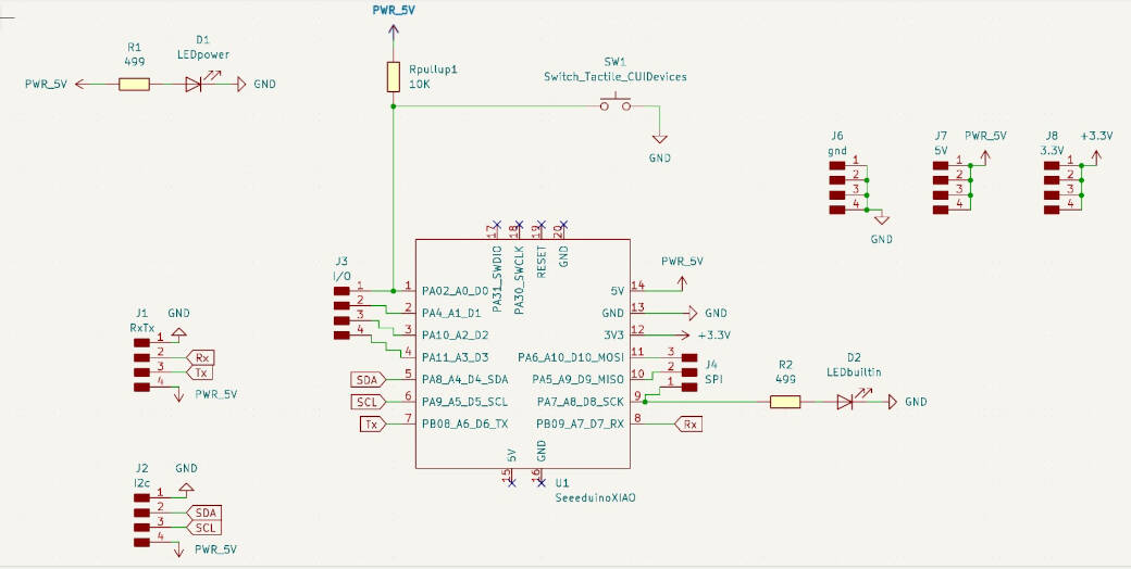
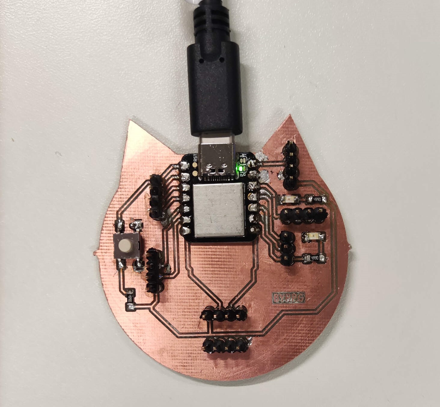
In KiCad, I downloaded the Fabacademy library, where I retrieved the correct model of the microcontroller I would be using (SeeeduinoXIAO). From there, I started building my board. The board is composed of the microcontroller, LEDs (so that I can program them later to test our PCB), a button, and different ports and resistors. This was designed in the schematic editor. To connect these components in an organized manner, I used the label tool, which connects them but does not display the line of the connection, thus making the schematic clear to look at.
Once I was satisfied with this design, I saved it. Then, on the toolbar at the top,
I clicked "open PCB in board editor" 
 . Once the new environment was opened, it was blank, and to retrieve the schematic information,
I clicked on the button at the toolbar "update PCB with the changes from schematic". A window popped up, and I clicked "update PCB".
. Once the new environment was opened, it was blank, and to retrieve the schematic information,
I clicked on the button at the toolbar "update PCB with the changes from schematic". A window popped up, and I clicked "update PCB".
From there, I had the components, but they were not yet placed in the correct locations. If you zoom in on the components using either, you’ll see white straight lines between the pins. These are called air-wires and tell you which pins to connect – according to your schematic. From this, I moved the components to their respective places so that they were closest to the pins they should be connected to. Note that you should try to arrange this in a way that the wires do not cross each other (this is not as important with a simple board, but it's good practice now for when I start making more complicated ones to simplify troubleshooting). To arrange the parts, I used the keyboard shortcut "M" to move and "R" to rotate.
creating the tracks
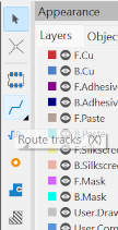
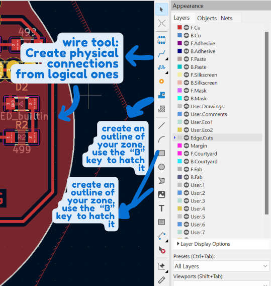
Once satisfied with my component placement, the next step I took was to replace the air-wires with copper traces by drawing tracks to connect the components. These tracks would form the conductive pathways on the finished board. To begin this process, I clicked on the "Route Tracks" button located on the toolbar, usually found on the right side, or pressed "X" on the keyboard as a shortcut. Then, I proceeded to draw tracks by clicking and dragging from one connection point to another, following the guidance provided by the air-wires. I continued drawing tracks until all air-wires were replaced, ensuring that every component was interconnected and there were no isolated "islands" of unconnected components remaining. This step is crucial for ensuring the proper functionality of the circuit on the final PCB.
Adding the ground plane and dboard outline
Connecting everything is not the only crucial step in this process.
I left all of my grounds disconnected from the microcontroller because I decided to create a ground layer which will connect all of the grounds together.
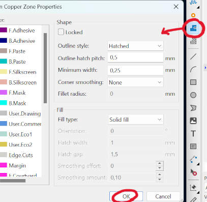
First, I created a 'zone' by clicking on the button usually located on the right toolbar.
When you hover over this button, it says 'Add a filled zone'.
You can also use the keyboard shortcut 'Ctrl+Shift+Z'.
With this, I clicked where I wanted to start the zone.
This action made a window pop up to edit the zone properties,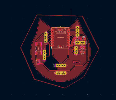 and I clicked 'GND' and hit OK. Next, I drew my zone and pressed 'B' to hatch it. Lastly, I drew the outline of the board.
Since I wanted to customize this shape into a cat outline, I created an arc to make the bottom part of the cat's head and used the line tool to create the ears and connect them to each other.
This outline I drew is the one the milling machine will cut through completely.
This means that there will be a tool change near the end of the milling process.
With the machine we have in the lab, I won't have to worry about the tool change because it happens automatically.
and I clicked 'GND' and hit OK. Next, I drew my zone and pressed 'B' to hatch it. Lastly, I drew the outline of the board.
Since I wanted to customize this shape into a cat outline, I created an arc to make the bottom part of the cat's head and used the line tool to create the ears and connect them to each other.
This outline I drew is the one the milling machine will cut through completely.
This means that there will be a tool change near the end of the milling process.
With the machine we have in the lab, I won't have to worry about the tool change because it happens automatically.
Exporting the gerber files
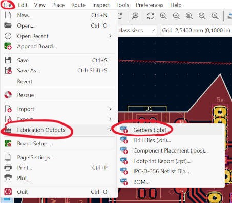
Once I was satisfied with my board, I exported the gerber files. To do this, I clicked on the top left corner of the toolbar, "File", and then "fabrication outputs" and then "gerber files". After this, a window popped up called "plot" where I selected all my preferred settings and chose where to save the files. Then, I clicked "plot" and then "generate drill files". And bam! I had my files ready, I saved a copy onto my USB stick and I was ready to mill my board.
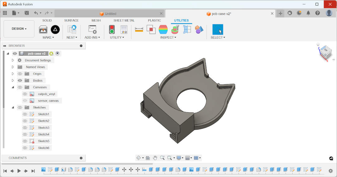
For the extra credits and to simplify things, I designed and 3D printed a case for the embedded programming assignment to hold the sensor and the PCB. I did this by exporting the edge cuts from KiCad as an SVG and importing it into Fusion 360 as a canvas. (I did this because when I imported it as an SVG, it was not to scale). With the canvas, I was able to "calibrate" the SVG to the correct size, and then I used the sketch tools to draw the case around the PCB and the sensor. I then extruded the sketch to the desired height and added a few fillets to the edges to make it look more polished. For the part that holds the sensor, I took a picture of the sensor and imported it into Fusion as a canvas, and then traced the outline of the sensor and extruded it into the PCB case with the option to "join" the two bodies. I also added a few other details to hold the sensor in place and a hole at the bottom of the PCB case so that I can push it out if needed.
The PCB production process
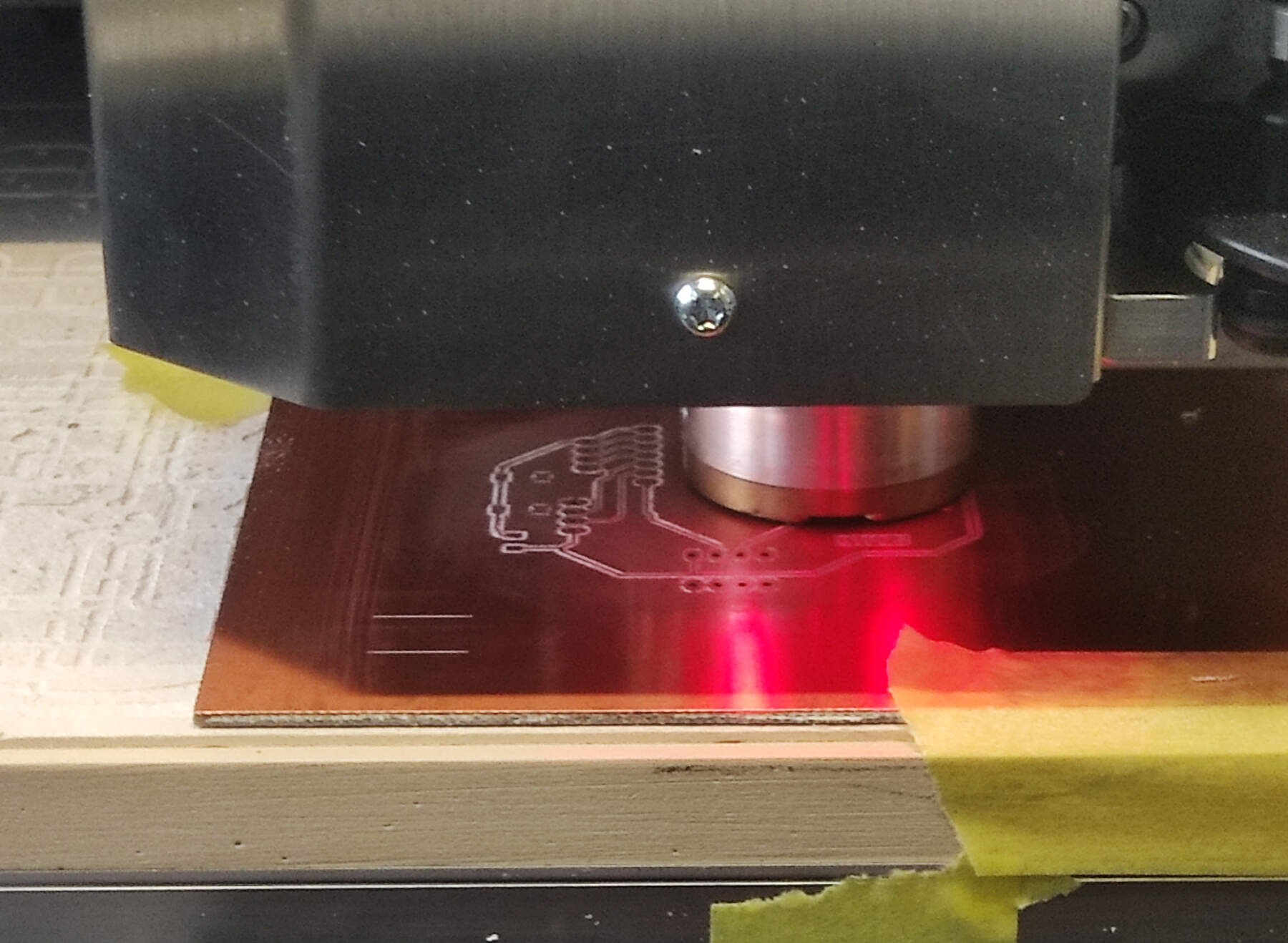
One of the machines we have at the lab (LPKF ProtoMat S104), which I used in the individual assignment part, uses gerber files in the software to control it. Therefore, I did not use MODS here; instead, I used KiCad. On Thursday, our instructor Ahmed introduced us to this software. We started by creating a simple board design, and later he showed us how to mill it.
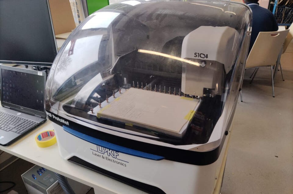
Milling The PCB Board
This is the software manual for Circuit Pro, the software we use to run on the CNC, I used this manual to study the parts I didn´t quite understand, it was helpfull. The controlls and navigation of the software is better documented in the group assignment page Here.
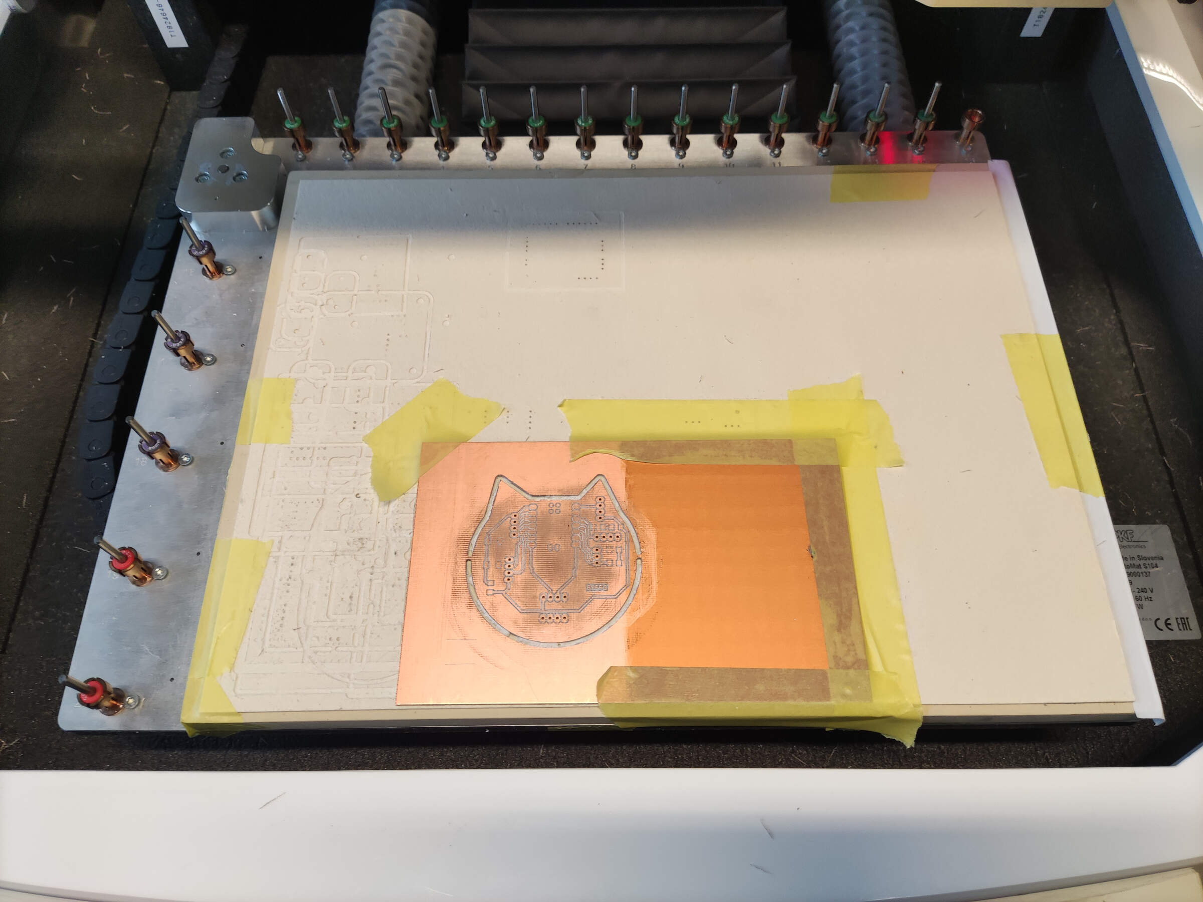
 After placing the board in the CNC machine, to make it adhere to the sacrificial paper layer on the machine bed, we use a weak painter's tape.
With our machine, we do not need to use double-sided tape, as there is a vacuum system to help secure the materials and remove dust. (its always good to tape down at least 3 points of contact)
After placing the board in the CNC machine, to make it adhere to the sacrificial paper layer on the machine bed, we use a weak painter's tape.
With our machine, we do not need to use double-sided tape, as there is a vacuum system to help secure the materials and remove dust. (its always good to tape down at least 3 points of contact)
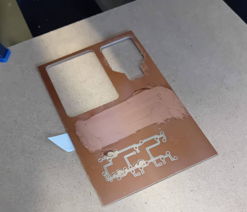
As you can see in this image, there is no dust (yay! no airborne fiberglass dust to inhale ;) )
Soldering
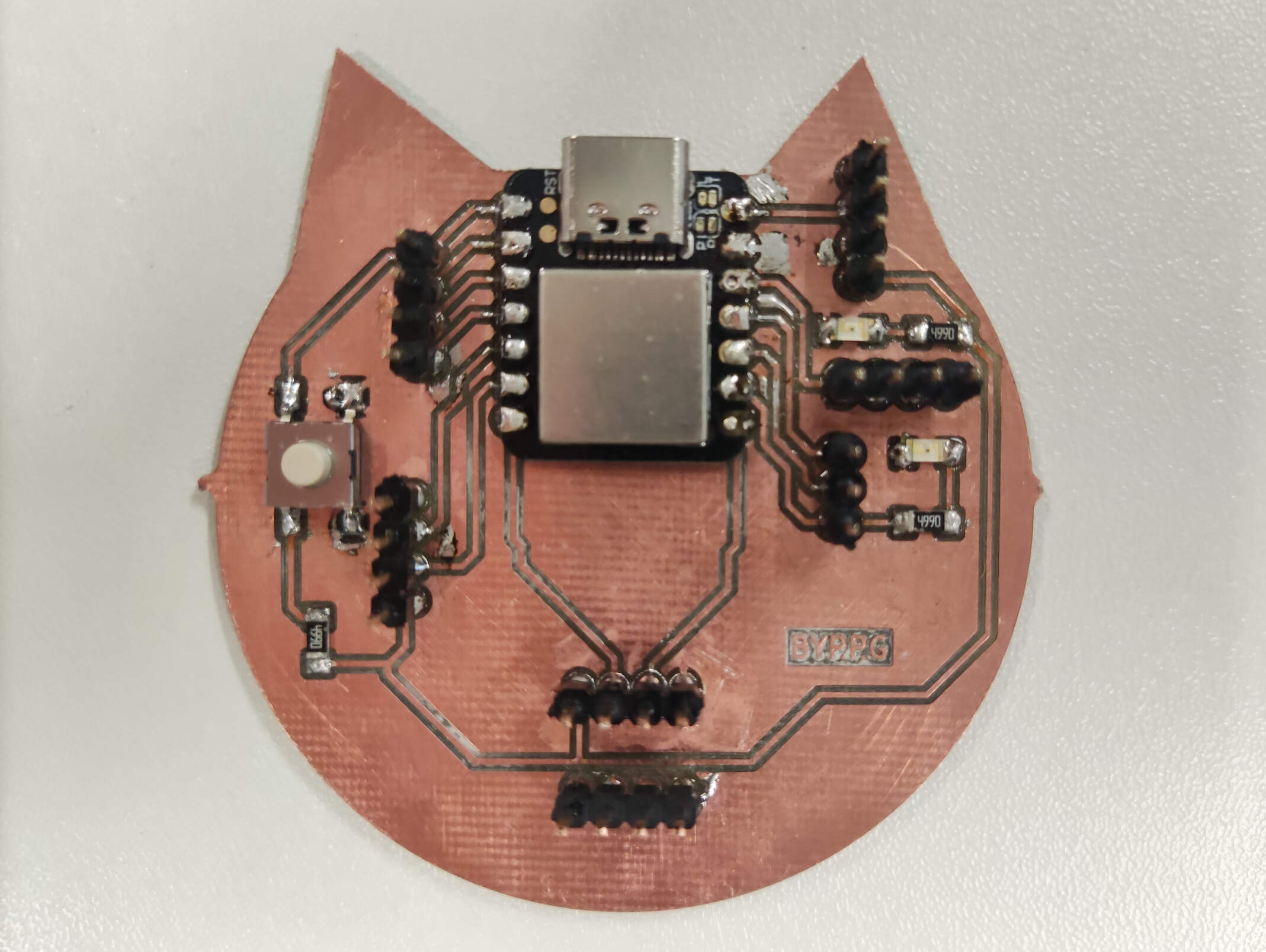
Components List
| Name | Description and data sheet | Quantity |
|---|---|---|
| Controller | Seeeduino XIAO SAMD21 | 1 |
| LED (R_1206) | Programable LEDs for testing | 2 |
| Resistor (R_1206) | 499Ω | 3 |
| Button | For testing the LEDs | 1 |
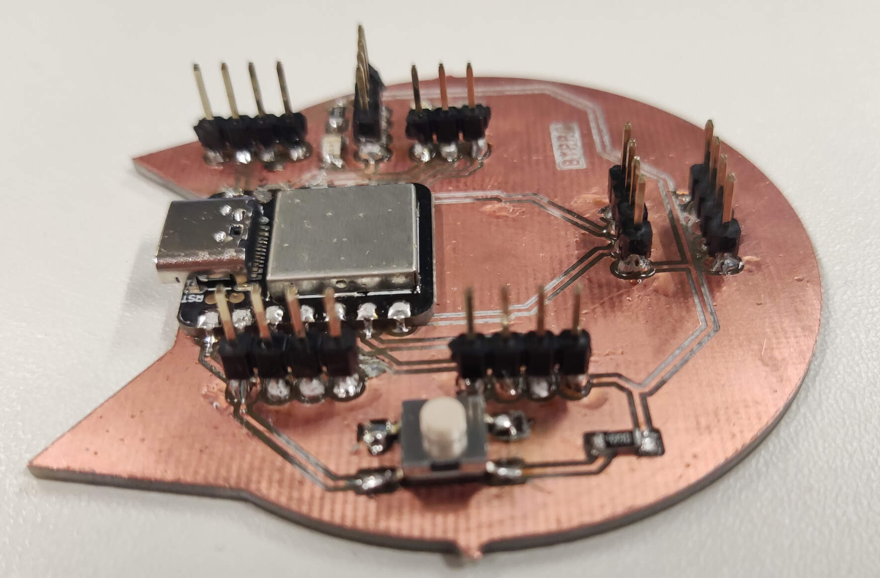
To start off with soldering, I first needed to separate the components necessary. To find out the specifications of each component, I consulted my schematic design for my PCB. I right-clicked on the components, and a little window popped up.
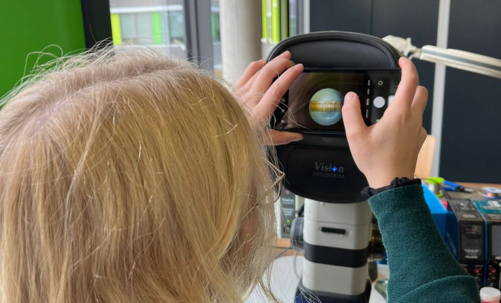
I went to "properties" and clicked on a link that sent me to the component's datasheet. For example, to find the correct orientation for the LEDs, the datasheet indicated the negative pole as the capacitor line, which is a fine green line on the actual LED. To further ensure this, I also checked it with a multimeter in the diodes setting.
| Soldering Station Setup |
|---|
| Fume Extractor |
| Workmat |
| Lamp with LED and magnifier |
| Anti Static Anti Magnetic Tweezer |
| Soldering station |
| Tin Copper alloy solder wire |
| Flux |
| Solder wick |

After this, I started soldering the components. I made a few mistakes, such as having an excess of solder in certain points, which risked the possibility of a short circuit. However, this experience taught me the wonders of using solder wick. Solder wick, also known as desoldering braid, is a thin, braided copper wire used to remove excess solder from electronic components and circuit boards. When heated with a soldering iron, the solder wick absorbs the molten solder, allowing it to be cleanly and effectively removed from the joint.
After soldering, I cleaned the board with a special WD40, to remove any residues like flux
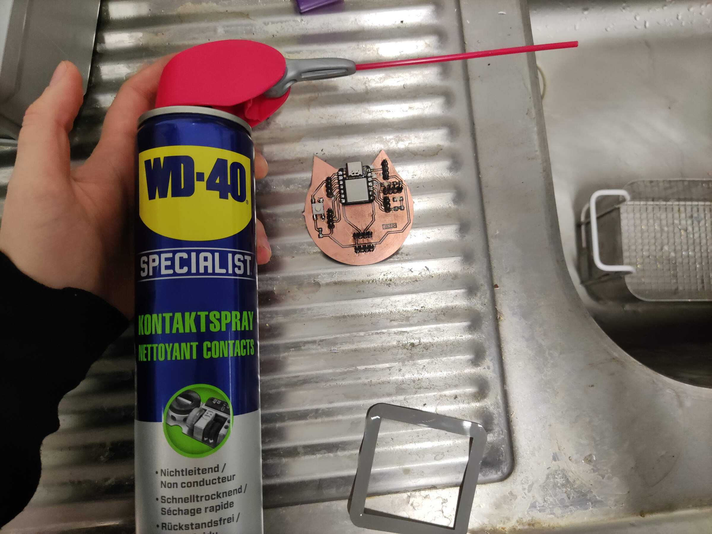
After applying the wd40, i left it for a while so it would evaprate... And just like that my PCB was done!... well amost ;) now I just had to check if it actually worked.
Testing
After soldering, I tested the board. I connected the board to my computer and opened the Arduino IDE, from there I uploaded a simple blink code to the board.
Huzzah!! it works