Electronics Production
Electronics production is a multifaceted process encompassing the creation, assembly, and testing of electronic components and devices. This dynamic field involves the transformation of raw materials and electronic components into functional products, ranging from simple circuit boards to sophisticated electronic systems. The production journey typically includes designing circuit layouts, fabricating printed circuit boards (PCBs), populating them with electronic components, and employing various manufacturing techniques to ensure reliability and efficiency. Quality control and testing play integral roles in the electronics production process, ensuring that the final products meet industry standards and perform optimally. As technology advances, electronics production continues to evolve, incorporating innovations that drive the development of cutting-edge electronic devices essential to our interconnected world.
- Characterize the design rules for your in-house PCB production process
- Send a PCB out to a board house
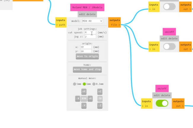
ROLAND MDX-40
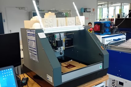
In the lab in Kamp-Lintfort there are two operating small CNC milling machines for milling PCBs: Roland M-40 and the LPKF.
Set Up
The set up of the machine consists of the Roland , the computer that is connect to it (used to control), and a vacuum cleaner for the milled material.
To initiate a milling operation, it is crucial to properly prepare the PCB material and secure it to the machine bed. The laboratory employs one-sided photosensitive FR-4 for PCBs, necessitating the removal of the photosensitive coating using acetone. To verify the absence of the photosensitive layer, observe a lack of shine on the material. Additionally, confirm that the material is of the correct size.
Prior to milling, inspect the cleanliness of both the machine bed and the interior of the Roland machine. Any debris between the bed and sacrificial layer or the sacrificial layer and the PCB material can result in surface irregularities and milling errors. It is essential to maintain a clean environment, as dust can compromise the adhesion of the double-sided tape used to affix the PCB material. Utilize a vacuum for cleaning the machine's interior thoroughly.
For securing the PCB material to the sacrificial layer, employ double-sided tape. If the sacrificial layer exhibits damage or unevenness, promptly replace it to ensure a level milling surface. Attention to these details will contribute to the precision and success of the milling process.
For securing the PCB material to the sacrificial layer, employ double-sided tape. If the sacrificial layer exhibits damage or unevenness, promptly replace it to ensure a level milling surface. Attention to these details will contribute to the precision and success of the milling process.
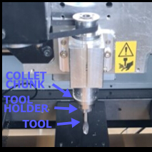
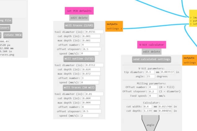
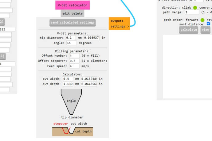
The subsequent step involves selecting the appropriate drill bit for the milling operation. Opt for a V-bit with a diameter of 0.4 mm and a 15° angle on the tip. When it comes to exchanging or inserting a drill bit, utilize two wrenches—one for the collet chuck and the other for the tool holder. Hold the collet chuck securely with one wrench while loosening the tool holder with the second wrench. Exercise caution to catch the tool once it is released.
IMPORTANT: DO NOT LET THE TOOL FALL DOWN! That can damage the bit severely, so it can not be used anymore.
Controls
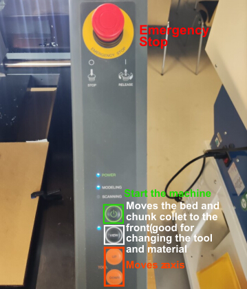
To Turn on the machine use the switch on the right side. Then use the start button on the panel. Open the Roland V-Panel on the computer. If the software shows an error of not being connected to the machine check if the Roland is turned on or if the USB connection is unplugged. For moving the CNC head use the speed options and the arrow buttons in the panel. NOTE: The control of the x-axis is the other way around as it moves the bed not the CNC head.
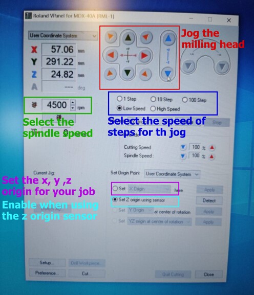
The subsequent step involves leveling the z-axis to establish the relative origin with respect to the material. Various approaches were explored for this purpose, with three methods tested. Initially, the paper method was employed, where a sheet of paper was inserted between the tool and the material. The z-axis was gradually lowered until the tool made contact with the paper, allowing for slight movement without resistance. This leveling technique proved effective, prompting the initiation of the first job, which involved characterizing the Roland machine.
However, the job was promptly halted by our local instructor who observed that the tool was cutting too deep. The excessive dust production and machine sound indicated the issue. The mistake was traced back to an oversight in the material thickness setting, which was subsequently corrected to 1.5 mm before restarting the job.
For the second attempt, an alternative approach was adopted—loosening the tool until it made contact with the surface and then tightening it again. Despite implementing this method, the tool failed to touch the surface during the job, necessitating another interruption. The underlying cause appeared to be a slight upward movement of the tool during the tightening process.
To address this issue, we implemented the z-leveling sensor as a final solution. In this process, the sensor is strategically positioned between the tool and the material, and the 'Set Z origin using sensor' function is activated in the VPanel on the computer. This initiates an automatic leveling of the z-axis. Through this method, successful leveling was achieved, paving the way for the completion of the initial cut—referred to as the characterization process.
Mods
The Mods Project is giving the possibility to create a .rml file out of an .png file. The .rml file is like g-code and gives information about the movement of the axis. It is a accepted file format for the Roland CNC machines.

Characterization
As previously stated, we utilized a file supplied by the Fabacademy for the characterization process and generated a fabrication output file using Mod. The completed characterization demonstrated impeccably clean edges, with no traces failing to connect, even when dealing with very high-resolution traces (0.001). This outcome indicates a high level of tool precision, a well-secured bed fixture, an undamaged tool, and accurate parameter settings. Due to the specified minimal cut width set at 0.02, there is no clearance available for thinner traces in the fabrication output file, and consequently, in the milling job as well. While the trace width of 0.001 remains visible, it is advised against using traces smaller than 0.07. This precaution is taken to avoid potential disruptions in the connections between components through the traces, ensuring the reliability and integrity of the electronic circuit.

LPKF ProtoMat S104
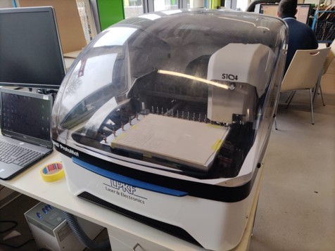
The second CNC machine for PCB milling in the lab, was the LPKF.
Set Up
The Setup of the LPKF consists of the CNC machine itself, a computer to process files and send jobs to the machine and a dust extractor.
To commence a milling operation, proper preparation of the PCB material and secure fixation on the bed are crucial steps.
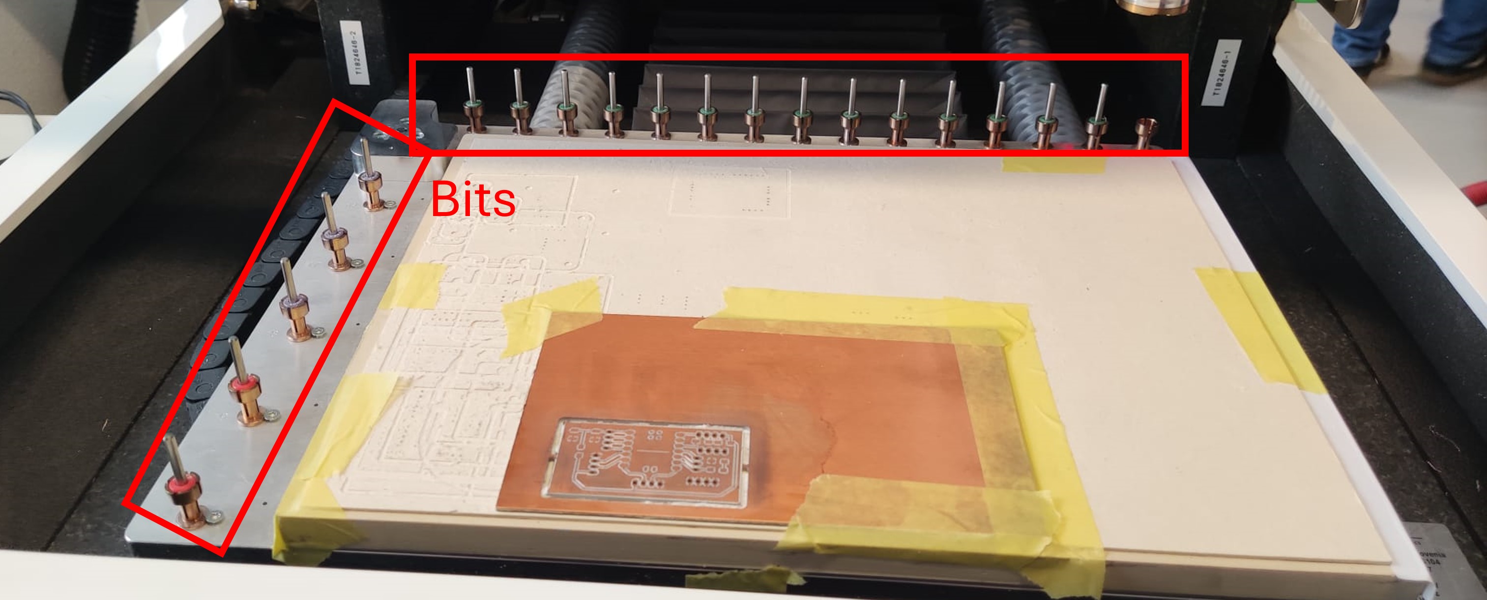
For both drill and milling bits, it's crucial to note that all bits are securely housed within the machine's enclosure, and the machine autonomously manages their use throughout the milling process.
Set Up
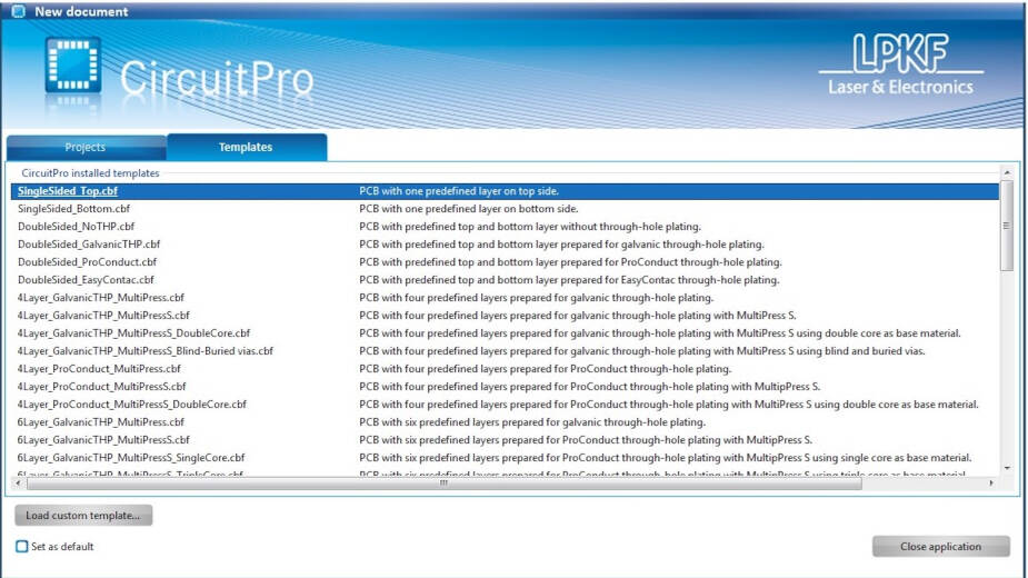
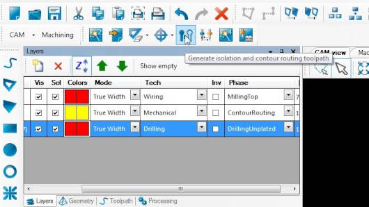
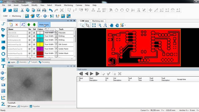
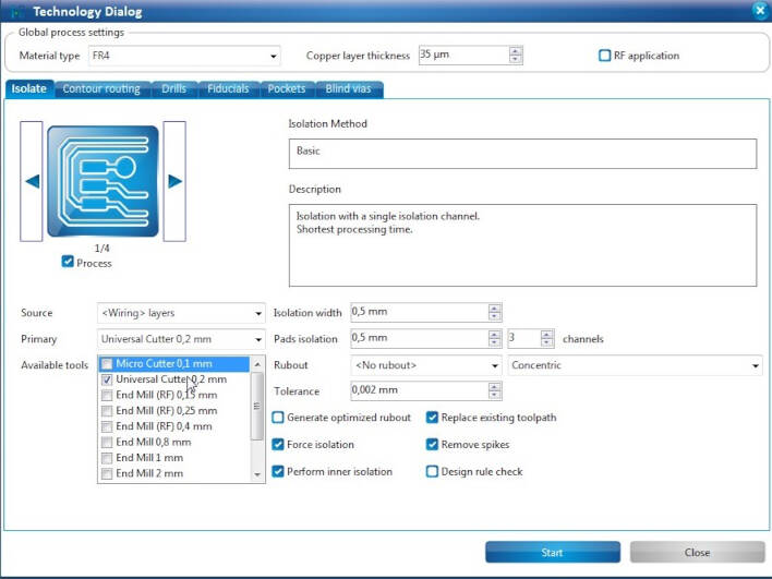
The machine is operated and job initiation is facilitated through the 'LPKF Circuit Pro PM' software provided by the company. To commence a job, follow the outlined steps below:
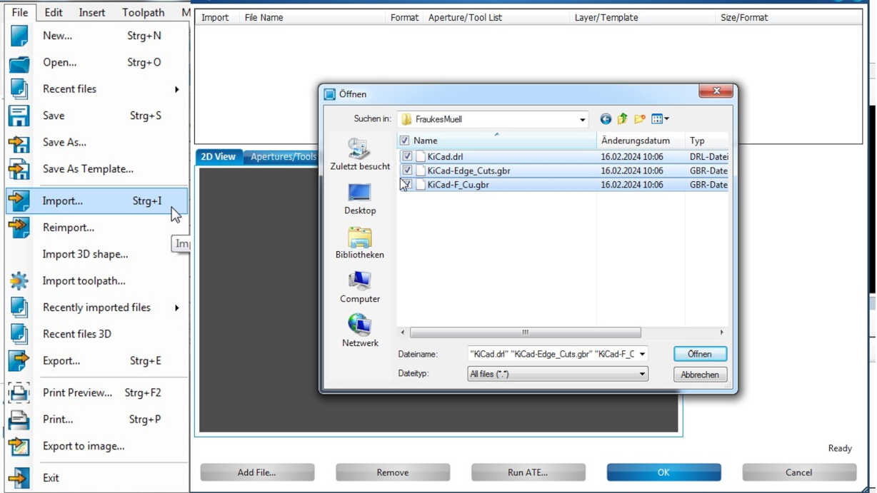
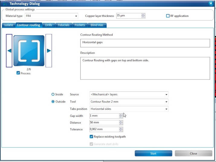
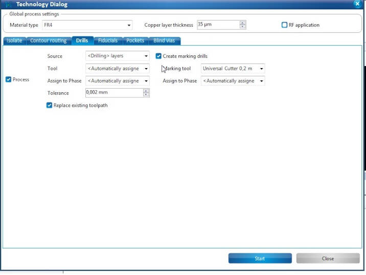
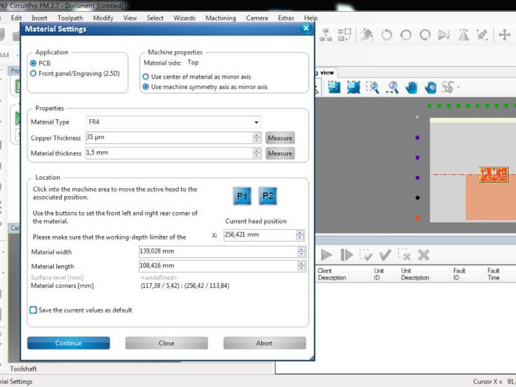
After these steps, save your job on the computer, as the machine can recover a job very easily and use the saved file, if problem occur. The machine will start the milling.
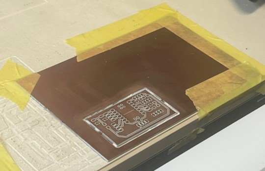
Characterization
As for the Roland MDX-40, we used a file that was supplied to us. However, instead of the .png, the LPKF uses gerber files that our instructor generated from the .png file we used on the Roland and by this supplied the file. After milling the traces with the software CircuitPro as described above, we obtained an incredibly precise milling. No trace failed. In contrast to the Roland, it was even able to mill out clearances up to the second smallest dimension, namely up t 0.02mm. This demonstrates a highly precise machining and precise automated steps of the LPKF. Nevertheless, as copper is still visible for all traces, milling each path once apparently is not enough to isolate the traces from each other. Similar to the Roland, it is advised to not set the trace and clearance width to the minimum of the possible range but instead increase it slightly to be safe. We propose traces and clearances should not be smaller than 0.05 mm, ensuring the reliability and integrity of the electronic circuit.
