13. Embedded Networking and communications
This week I worked on Networking and Communications Assignment
Assignment
Individual assignment:
  design, build, and connect wired or wireless node(s)
  with network or bus addresses
Group assignment:
send a message between two projects
Inividual Assignment
For this assignment, I reviewed my colleague’s Nervene Bhagwandass, assignment, of same. Upon doing this, I observed that he as well reviewed Adrian Torres, and took inspiration for these assignments. The basis of this assignment, was to design and manufacture two boards to communicate with each other. I was able to achieve this by creating two boards: * Bridge * Node
These boards would utilise the serial bus method of communicating with each other. Mainly, via the TX and RX pins/ ports on the microchip. The TX port is used to “Transmit” signal, where as the RX port is used to “Recieve” signals. The microchip of choice for this assignment was the faithfull ATTiny 412.
Process
The process of designing, milling and soldering these boards, was very simialr to previous electronics assignments, in that, Fusion 360 was utilised to achive the design, Carbide Create was used to set up and edit for milling and lastly, Carbide Motion was used to perform the actual milling process. More of this is seen in the following images seen further in the assignment documentation, as it progresses.
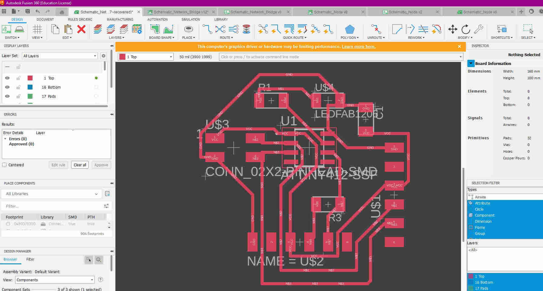
The Image above shows the schematic of the Bridge PCB, designed in Fusion 360, that utilises the ATTiny 412 Chip
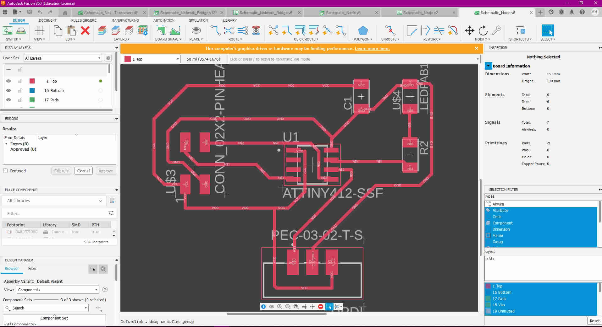 The image above shows the schematic of the Node PCB, designed in Fusion 360, that also utilises the ATTiny 412 Chip
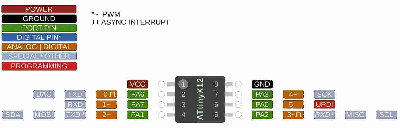 And here we have old reliable, the ATTiny 412 Pinout, which always serves as the ideal guide when allocation I/O’s, as well as determining where our TX & RX pins can be configured.
The components used for this assignment were as follows: * 1 kΩ resistor (X2) * 4.99kΩ resistor (x1) * 1uF capacitor (unpolarised) (x2) * Green & Red LED (x2) (1 Each) * 2x2 Vertical Conn Header (x2) (used for the serial bus connection) * 15 Pin Conn Header (broken into 6 x 6 x 3, for FTDI and UPDI repsectively) * 2 ATTiny 412 Chips
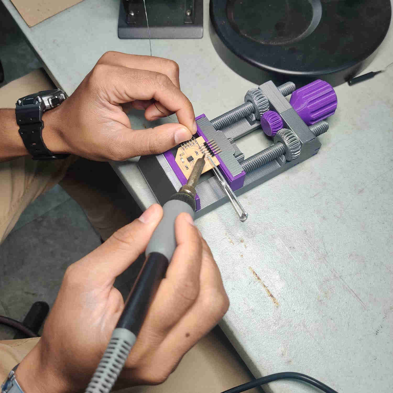
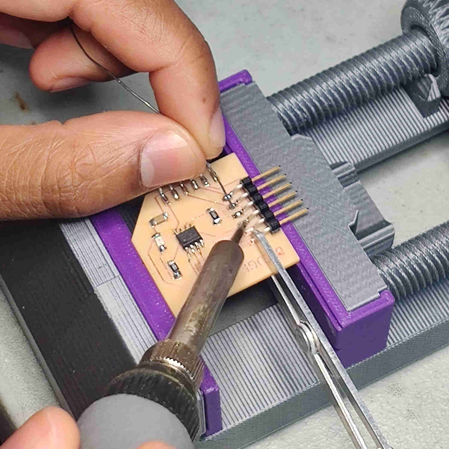
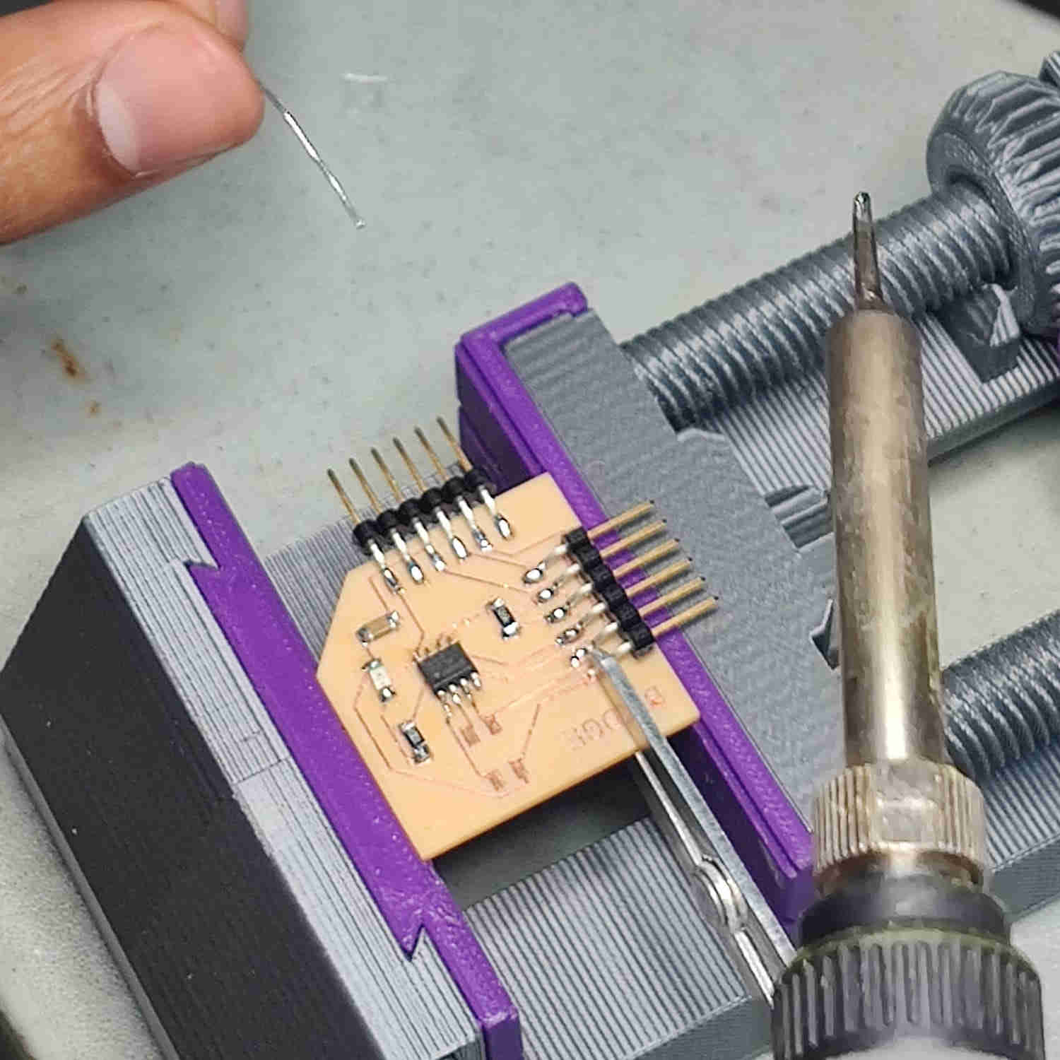
Once the milling was completed, with the aid of Carbide Create and Carbide Motion, the soldering procees was done. The following images/ video, just showcase myself soldering my components to the Bridge board.
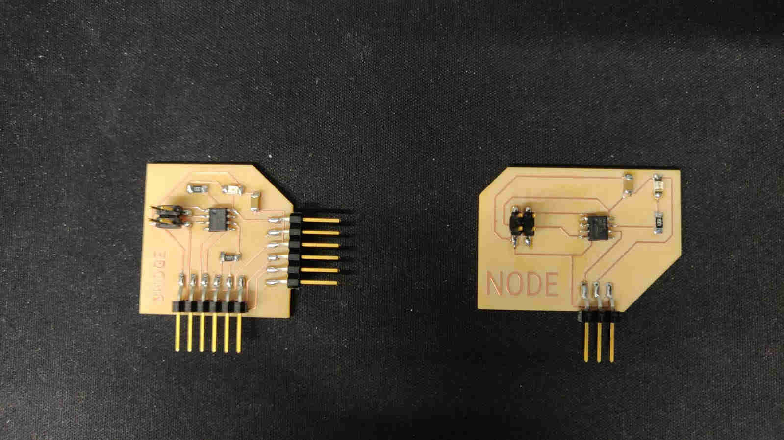 And here we have our complete boards, the Bridge and the Node.
Programming
At this point, it’s a no braier that the programming app of choice would undoubtly be the Arduino IDE. As I’ve used this app for previous assignments, I’ve grown to understand and appreciate the versatility of it.
Bridge
Firstly, I had to program the Bridge board. To do this, I connected the FTDI cable directly to the FTDI conn header (seen on the southern side of the Bridge PCB). Below, is the sketch that was used for the Bridge program.
#include <SoftwareSerial.h>
SoftwareSerial mySerial(0,1); //RX, TX
int v=0;
int nodeid=1; //Node Identification
int i=0;

void setup() {
  mySerial.begin(115200); //initialize serial communications
  pinMode(4, OUTPUT); // led
}

void loop() {
  for (i=1;i<=3;i++){ // initialization; condition; increment
  mySerial.println(i); // print value to Serial
  delay(1000);
  }

  while (mySerial.available () == 0 ) {}  //while serial is 0
  v = mySerial.parseInt();
  if(v == nodeid)        //If the value of v equals the identification of the node
{
  digitalWrite(4,HIGH);   // LED comes on
  delay(200);       // Indicates time between on/off
  digitalWrite(4,LOW);   // LED comes off
  delay(200);    // Indicates time between on/off
}
else
{
  digitalWrite(4,LOW);   // keep LED off
 }
}
Once uploaded, I knew that the sktech would be saved within the chips memory. I ensured prior to soldering, that the Bridge PCB would be equipped with a RED LED to distinguish it from it’s “colleague” the Node.
Node
Similarly, for the Node PCB, using the Arduino IDE, I uploaded the skecth to the Node PCB memory. This time I connected the UPDI adapter module to the UPDI pins on the board. Below is the aforementioned sketch for the Node.
#include <SoftwareSerial.h>
SoftwareSerial mySerial(2,3); //RX, TX
int v=0;
int nodeid=2;//Node Identification

void setup() {
  mySerial.begin(115200); //initialize serial communications
  pinMode(4, OUTPUT); // led
}

void loop() {
  while (mySerial.available () == 0 ) {} //while serial is 0
  v = mySerial.parseInt();
  mySerial.println(v);
  if(v == nodeid)     //If the value of v equals the identification of the node
{
  digitalWrite(4,HIGH);  // Put LED on
  delay(200);           // Indicates time between on/off
  digitalWrite(4,LOW);  // Put LED off
  delay(200);           // Inicates time between on/off
}
else
{
  digitalWrite(4,LOW);   // Turn LED off
 }
}
Again, to distinguish the Node, I added a GREEN LED to the PCB prior to soldering.
Once both programs were uploaded to thier respective boards, it was time to test. To achieve this, 4 jumper wires were used. This is how they were connected to fulfil the SERIAL BUS connection.
- ORANGE connected VCC>VCC
- YELLOW connected GND>GND
- BLUE connected RX>TX
- GREEN connected TX>RX
This is seen in the short video below:
PCB Files
Group Assignment
The Group Assignment was to send a message between two projects, this can be found here.