8. Electronics production
This week I worked on defining my final project idea and started to getting used to the documentation process. For this weeks assignment, we are required to mill, solder, test and program our own PCB boards.
Group Project
Individual assignment:
  make an in-circuit programmer that includes a microcontroller:
     extra credit: customize the design
     mill and stuff the PCB
     test it to verify that it works
     extra credit: try other PCB processes
# Milling My PCB
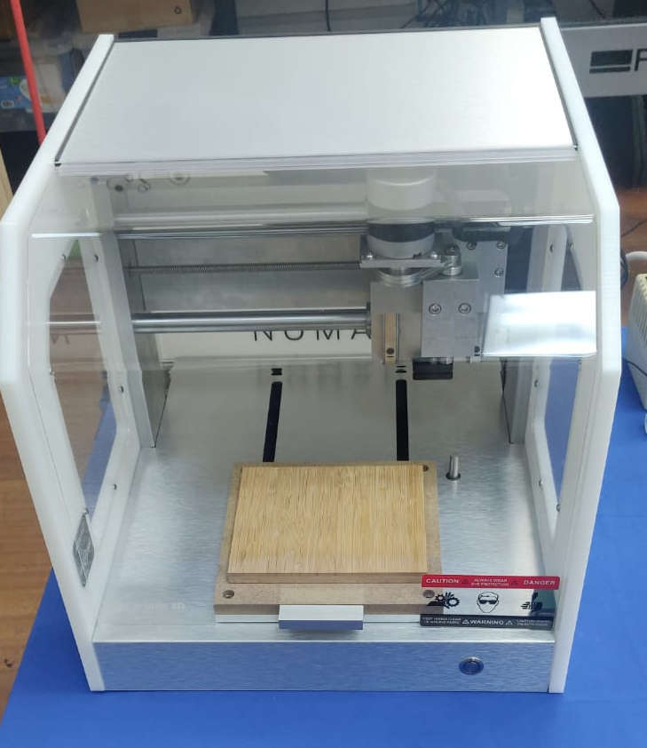
For this milling proces, we used the NOMAD 3 desktop milling machine to mill our PCB boards. As this machine was very new to us, we viewed the processes of setting it up and understanding the elements behind the milling process. The interface used for the Nomad 3 was the Carbide Motion. This piece of software allows us the ability to virtually mill most materials within the constraints of the machines workspace MDF wasteboard (8″ × 8″ × ½″)

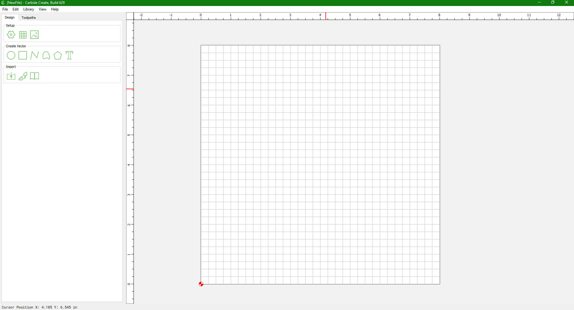
An additional editing and creating app/ software was included with the NOMAD 3, to work in tandem with the Carbide Motion. This app is called Carbide Create, and it provides a user friendly environment that would definetely appeal to any tinkerer/ engineer/ hobbyist/ technician. It possesses a plethora of easy to use features, from creating vectors with preset shape templates, to utilising boolean functions to manipulate various designs.
Both the Carbide Create and Carbide Motion came with simple step by step tutorials, that perfectly guides the user to understand the operation and features of the machine. I viewed these tutorials, and applied some of the proceduresI learnt towards the production of the PCB.

# Editing of PCB (Milling PCB Cont’d)
To actually achieve the milling of the PCB, I was guided by my Instructor Jason Wang of the Vancouver FabLab to utilise the USB-FT230XS-serial.traces, with the Nomad 3 CNC machine. (Note: While setting up our Nomad 3 CNC Milling machine, it was discovered that the collet ER-11 was missing from our package, as such, we weren’t able to actually mill the PCB board at this point in time)
The following are the steps to edit the PCB:
-
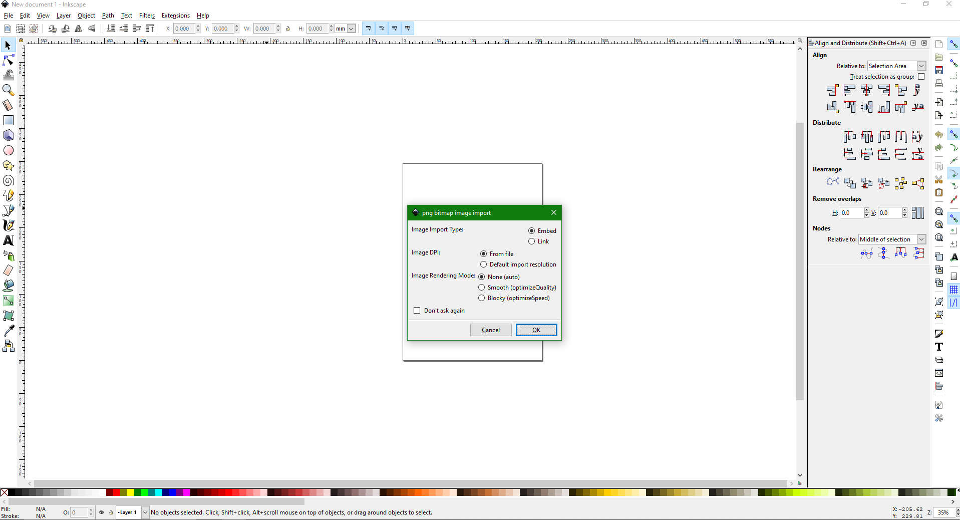
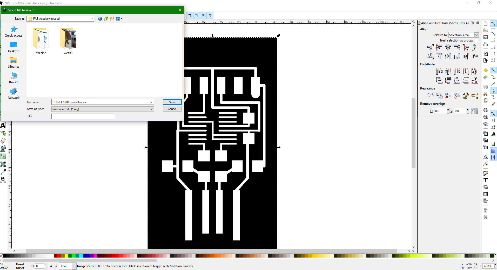
First, open the saved PNG image in INKSCAPE, ensure that image import type is select to Embed
-
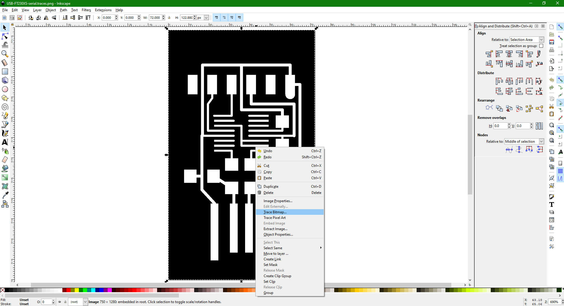
Next, select the image, right click on it and select “Trace bitmap”
-
The default settings should suffice, click ok

-
Seperate the traced shape from it’s original. the original is on the left and the traced is on the right

-
Save the traced image as .svg
-
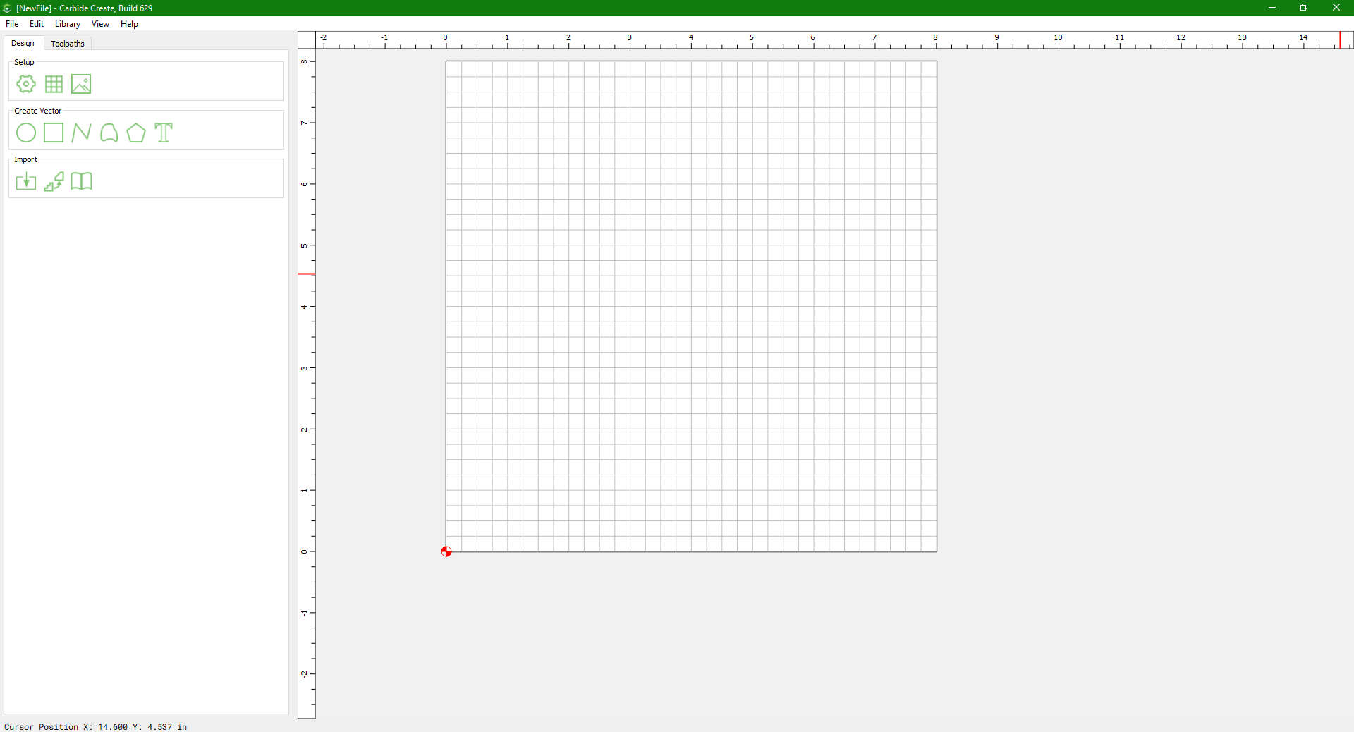
Next, open Carbide Create
-
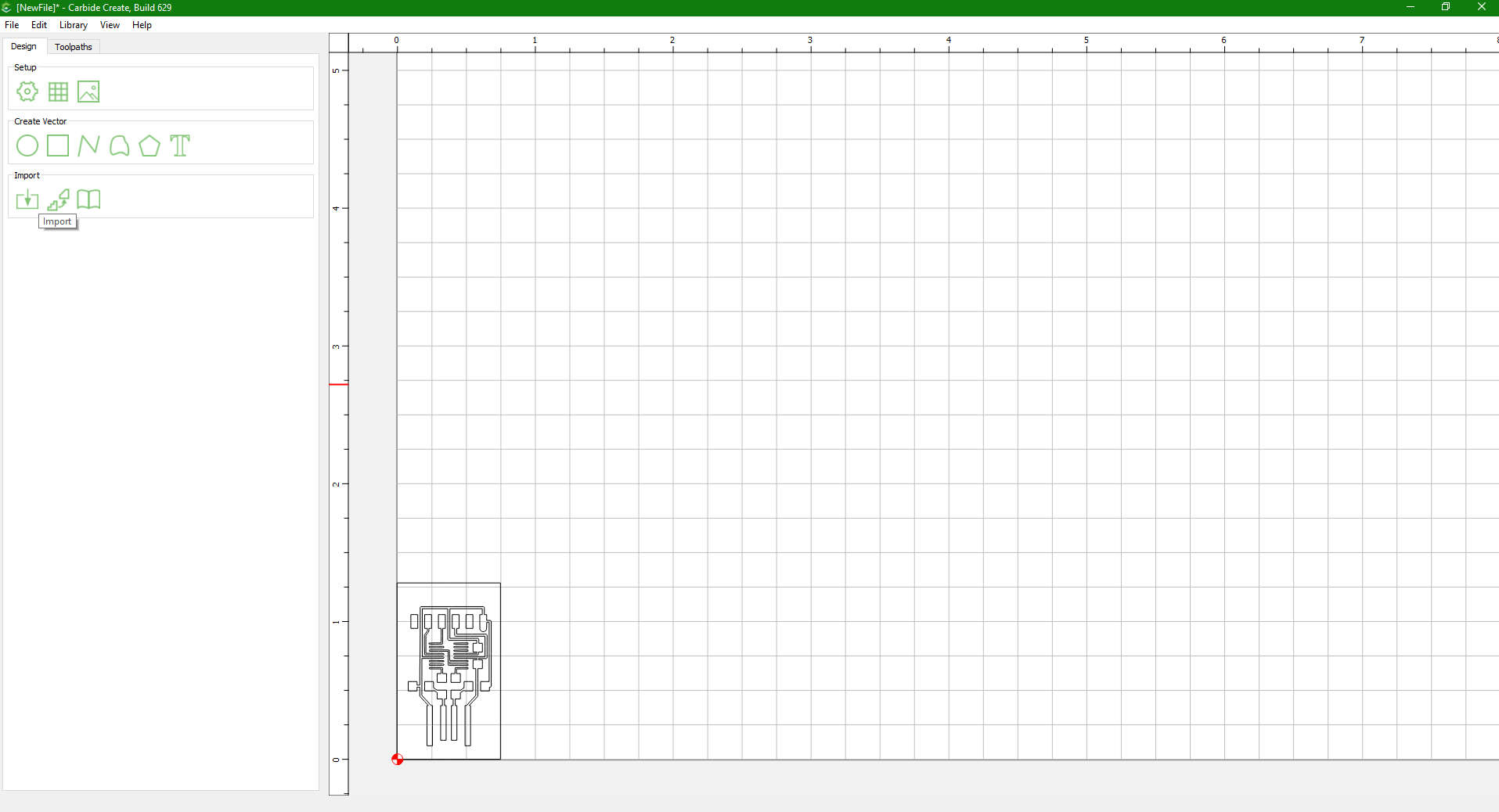
Import the svg file created in Inkscape
-
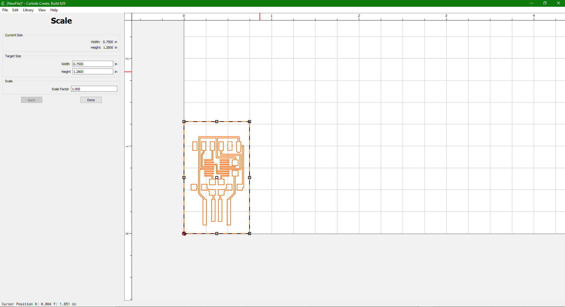
Select or highlight the svg file and select scale to check the scale size

-
Ensure the Current size is identical to the PCB size
-
Select the toolpaths tab
-
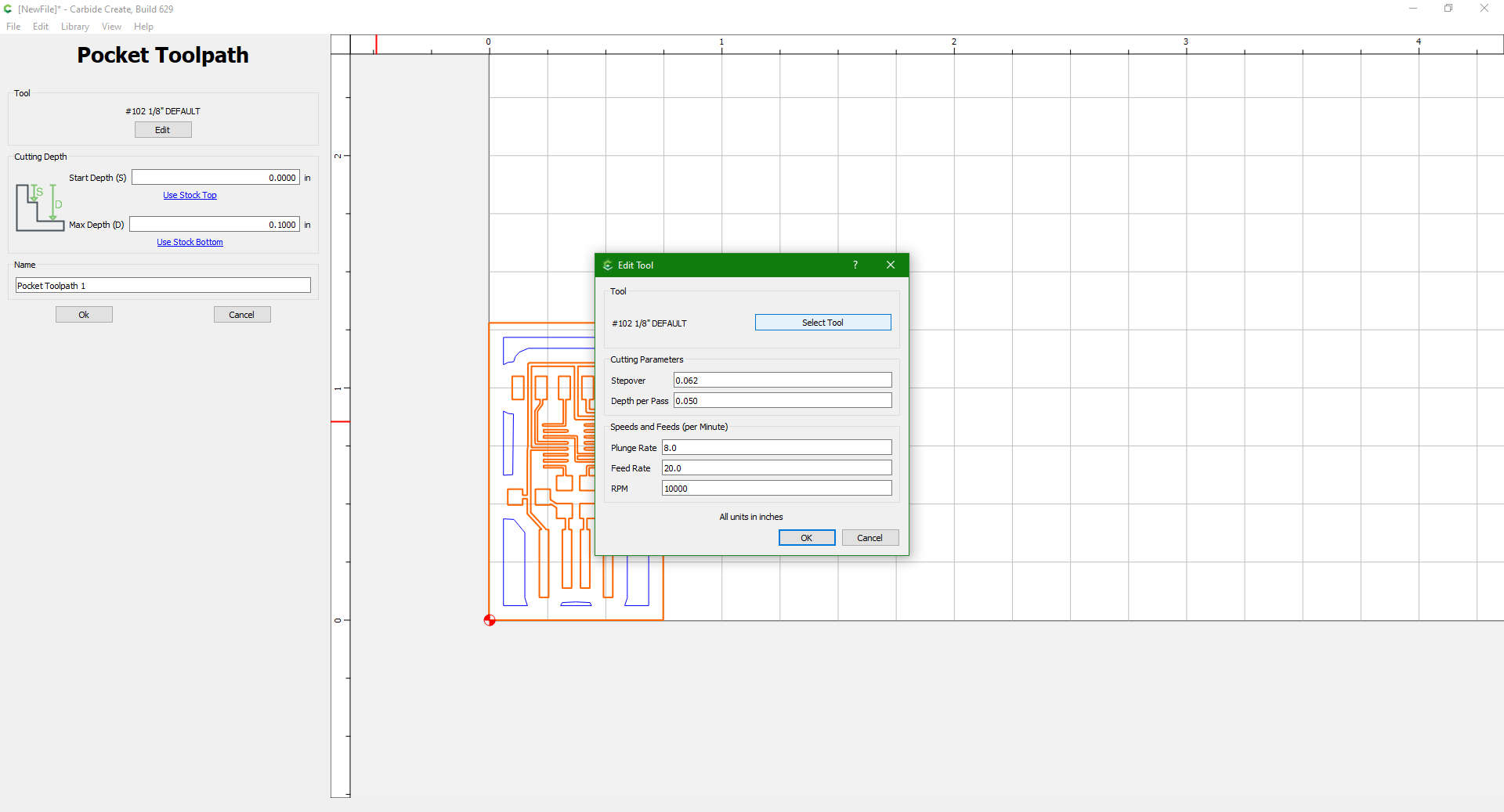
Select/ highlight the PCB and click pocket

-
In the Pocket toolpath, select the “edit” option under tool

-
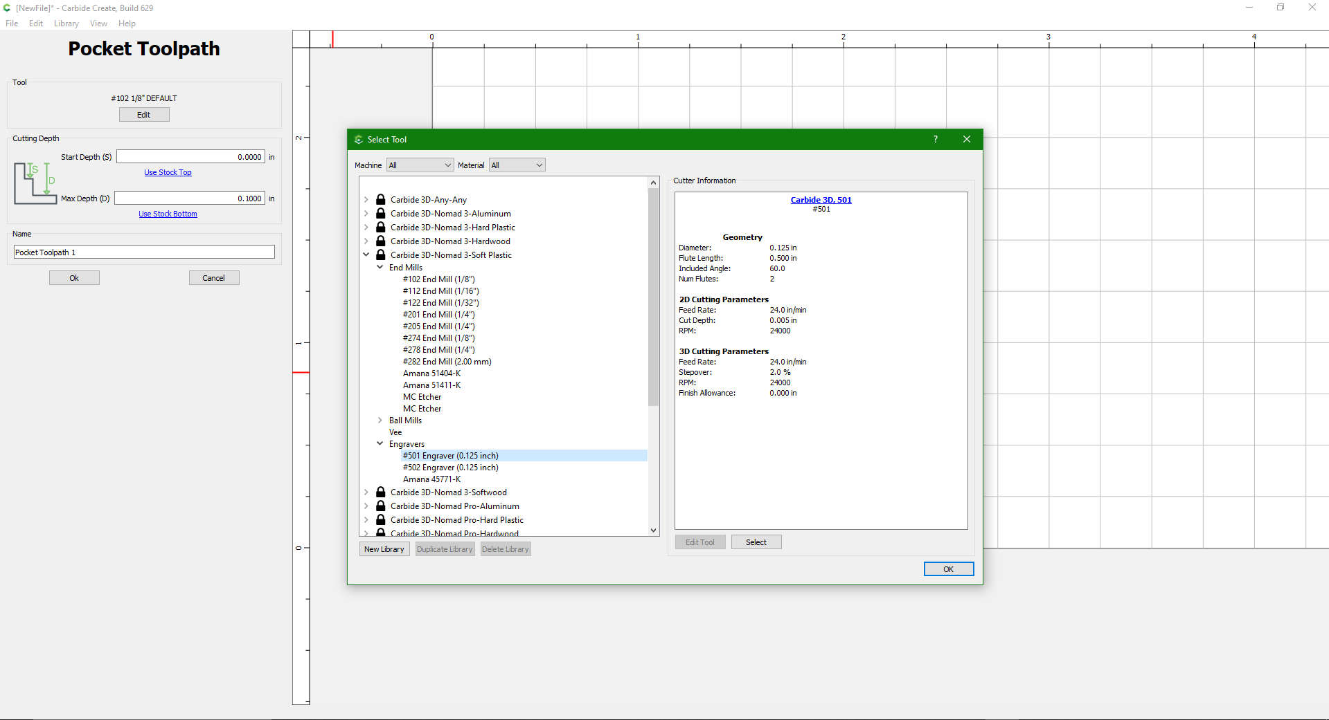
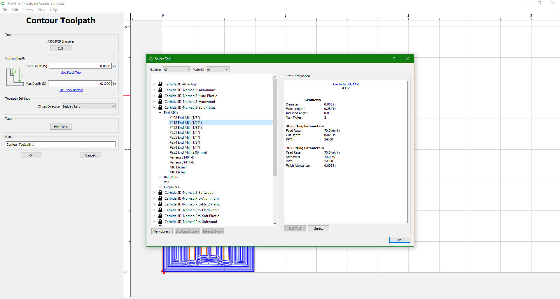
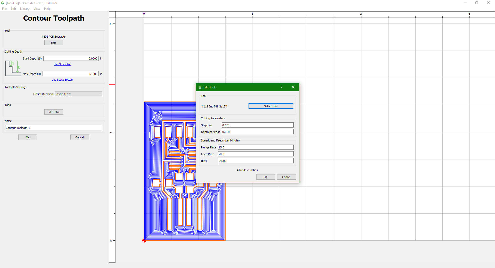
In the “Edit Tool” window, click “Select Tool”
-
In “Select Tool”, find “#501 Engraver” under “Carbide 3D Nomad 3 Soft Plastic> Engraver.” These are the parameters we need for creating a new tool profile for PCB milling. The reason we need to create a new profile for 501 bit, is because we need to use it as End Mill in place of Engraver.
-
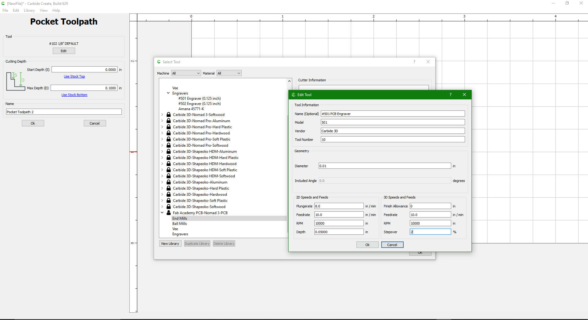
Click “New Library” at the bottom left corner, and create a new category.

-
Under the new category, right click on “End Mills” and select “Inch” under New Tool>End Mill>Inch.

-
Input the information we saw for the #501 bit into the field. (Or follow the photo below.) For the feedrate, 10 in/min is pretty conservative, 2 or even 3 times of the speed should also work, but let’s start safe.
-
After creating the 501 toll profile, select that, and click ok.

-
Before clicking ok again, copy the number under “Depth per Pass”. Then click OK.

-
Under “Max Depth”, put in the “Depth per Pass” number we just saw. This will be our starting point, and the theoretical cutting depth to cut the width we input in the “Diameter” in the tool profile. We can increase the Max Depth to get a thicker cut, or decrease it to get a thinner cut, in theory. Click OK.

-
We should be able to see the tool path that will take out the unwanted copper.
-
Select only the outer path, and click “Contour”, we will create the cut out tool path now.
-
Select #112 under Soft Plastic. (Use a thicker or thinner end mill to achieve this, depending on your PCB’s shape, use some discresion.) Click OK.
-
Double check the number and click ok
-
Input the PCB’s thickness in “Max Depth”, then click ok
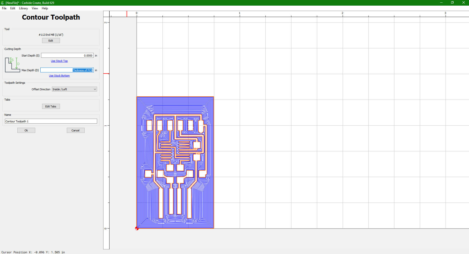
-
Now we have both tool paths for milling and cutting the PCB, Click “Save GCode”.
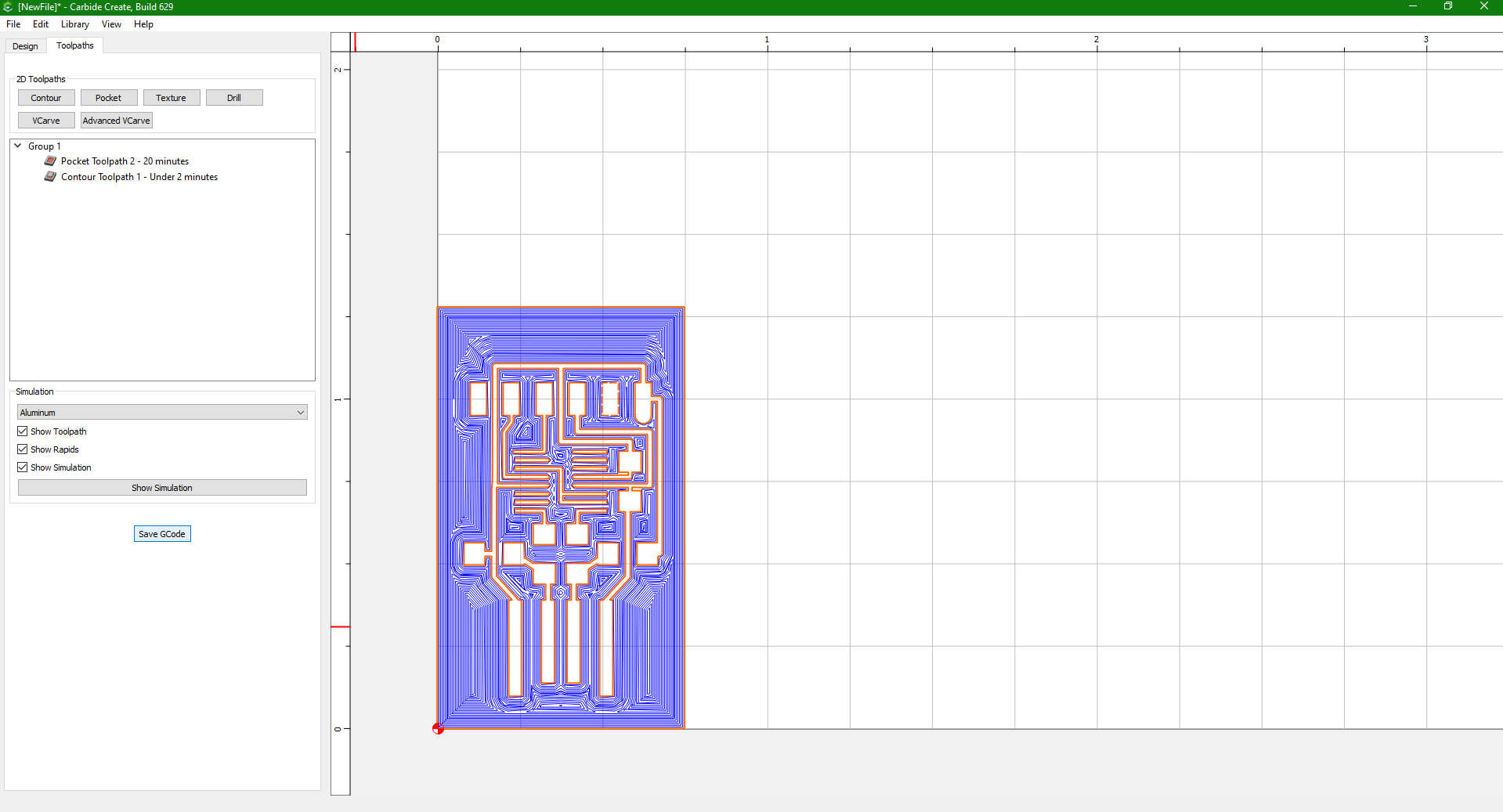
-
Save GCode

-
Select “Carbide 3D Nomad Pro” under Post Processor. Then Click ok and save the file
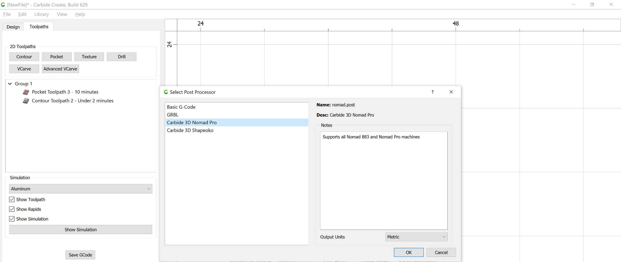
-
The GCode .nc file that we would use to mill the PCB, can be found here
” As mentioned earlier, due to the abcense of the collet chuck, the machine was not able to mill my pcb board, however, this will be done when one is aquired, until then, testing of the PCB is put on hold…But not for long..”
Useful links/ apps
Update!
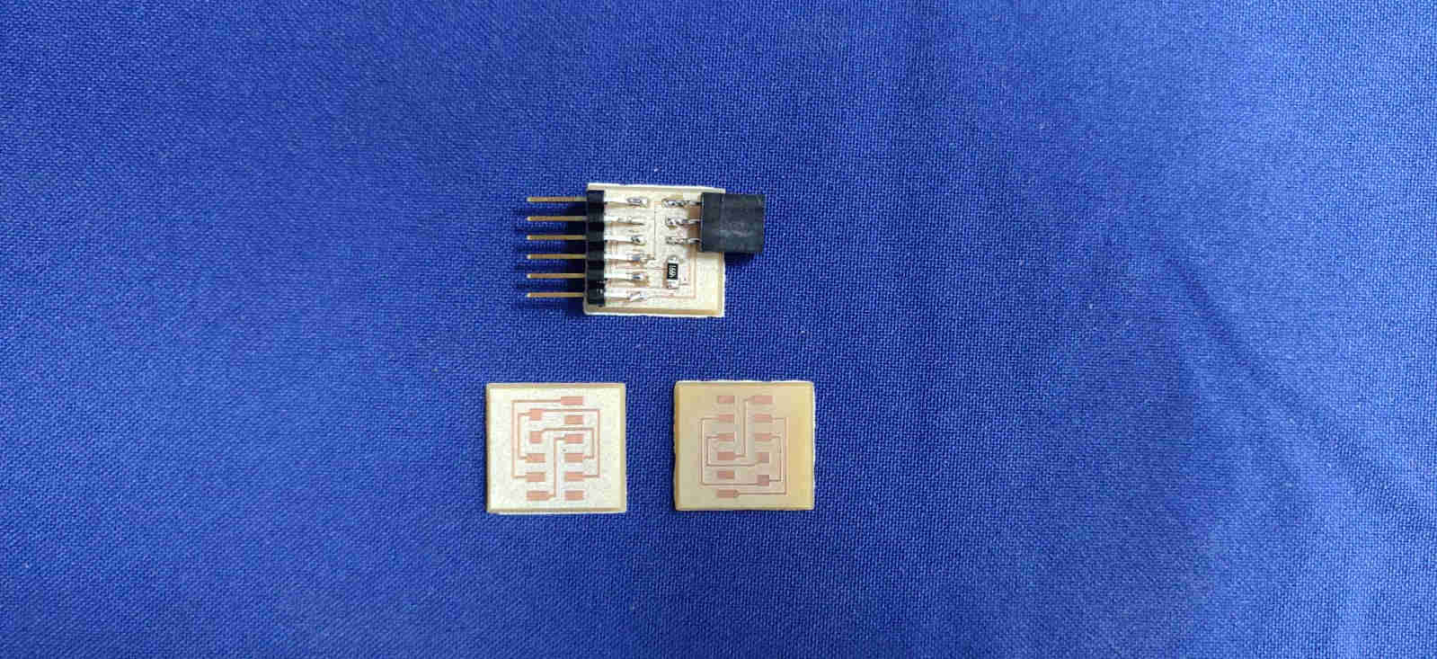
Within the week of the Electronics Design week, thankfully a collet was sourced, purchased and installed, that matched the Nomad 3. I was able to mill my PCB board, but opted to use the UPDI design instead of the FTDI as mentioned earlier. I used the same procedure to convert my UPDI found here @ Adrianino, and utilised Inkscape to ensure the traces were visible, when the png file was converted to a bitmap.

I must admit, there was great difficulty in determining the exact correct depth of which to set the 501 PCB Engraver, was quite a challenge and very time consuming. A good bit of resources were used up in the process of finding the precise depth to work with, ergo, mostly PCB boards.
Alas, I was finally able to get the right cut, and save the cutting parameters; Depth per pass, stepover, tool depth, etc, As well as the GCODE. The finished product was then soldered and an additional two copies of the UPDI were milled just in case of any mistakes whilst the soldering process was done.
Components used for the UPDI: - 499K Resistor, 6 Prong Header/ Connector, 3 Pin Connector


Upon Completion of soldering, I tested my UPDI board for continuity, with a FLUKE Multimeter, ensuring it works.
PCB REDESIGNED
Assignment
Group assignment:
 characterize the design rules for your in-house PCB production process
  send a PCB out to a board house
Individual assignment:
  make and test the development board that you designed
     to interact and communicate with an embedded microcontroller
  extra credit: make it with another process
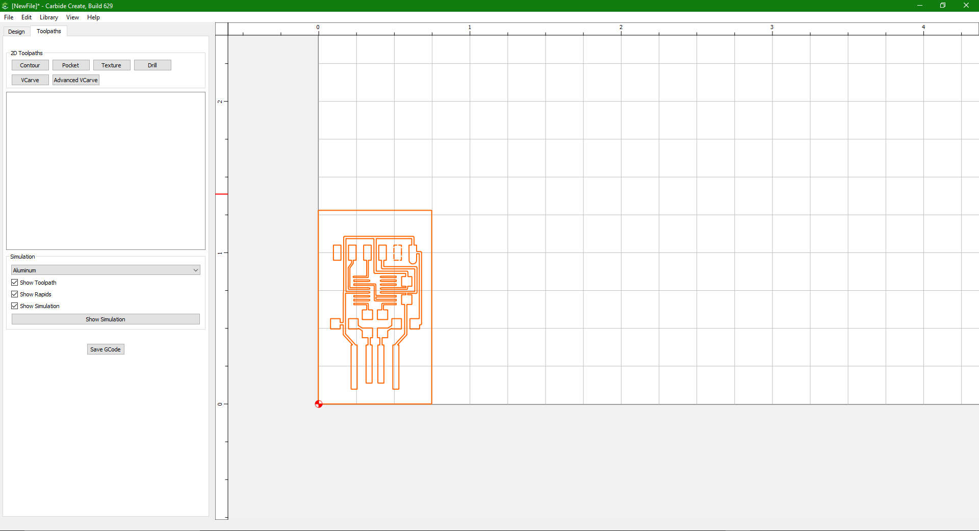
For the Individual Assignment, I decided to do two redesigns of the previously seen PCB in this assignment. I utilised Fusion 360 to accomplish this( as seen in the images below).
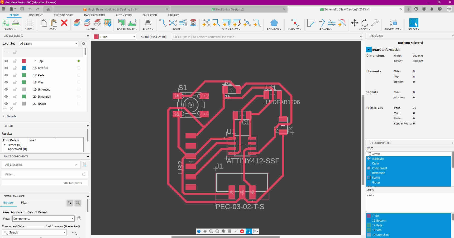
Redesigned PCB

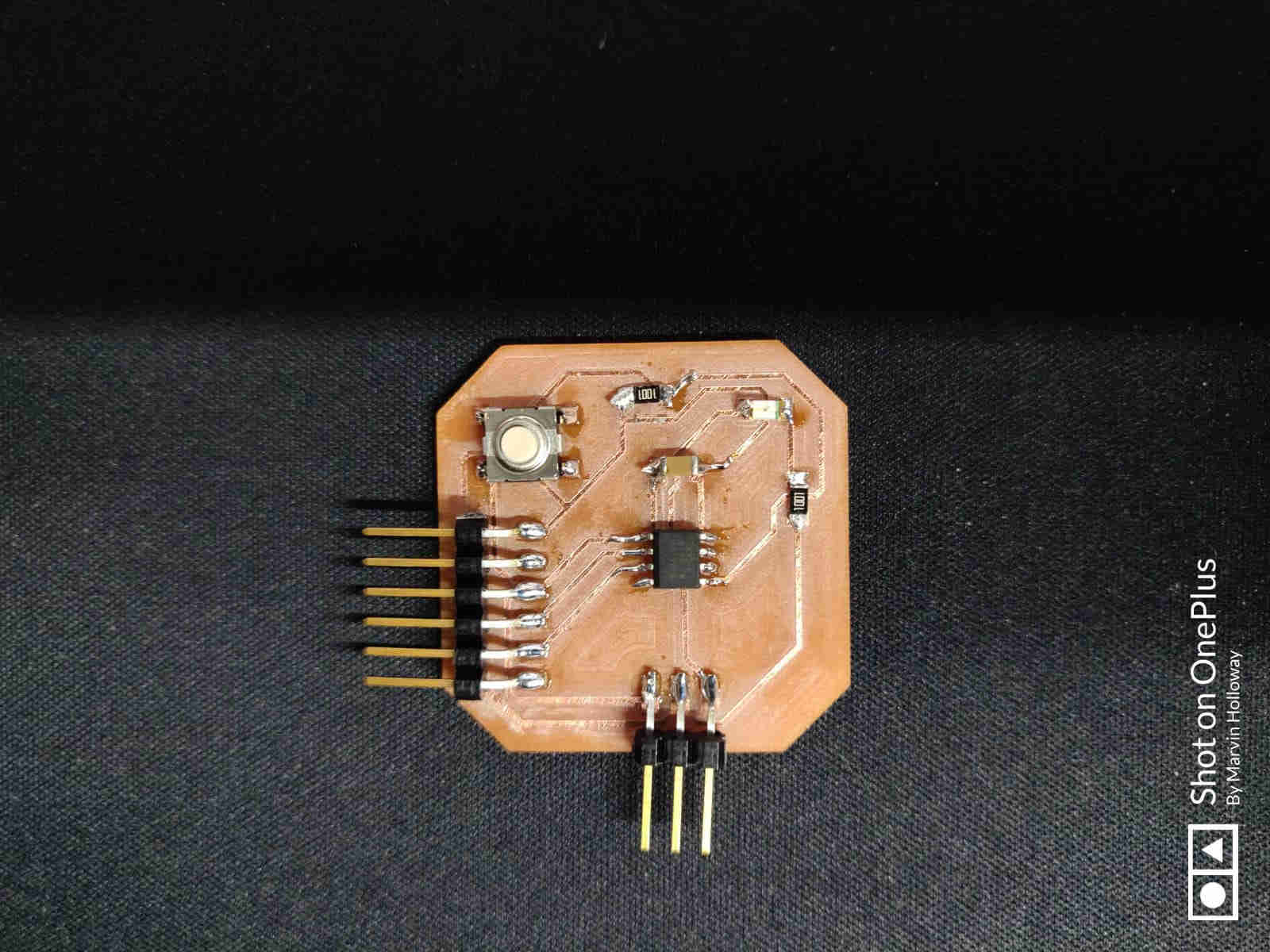
SUPERMAN PCB
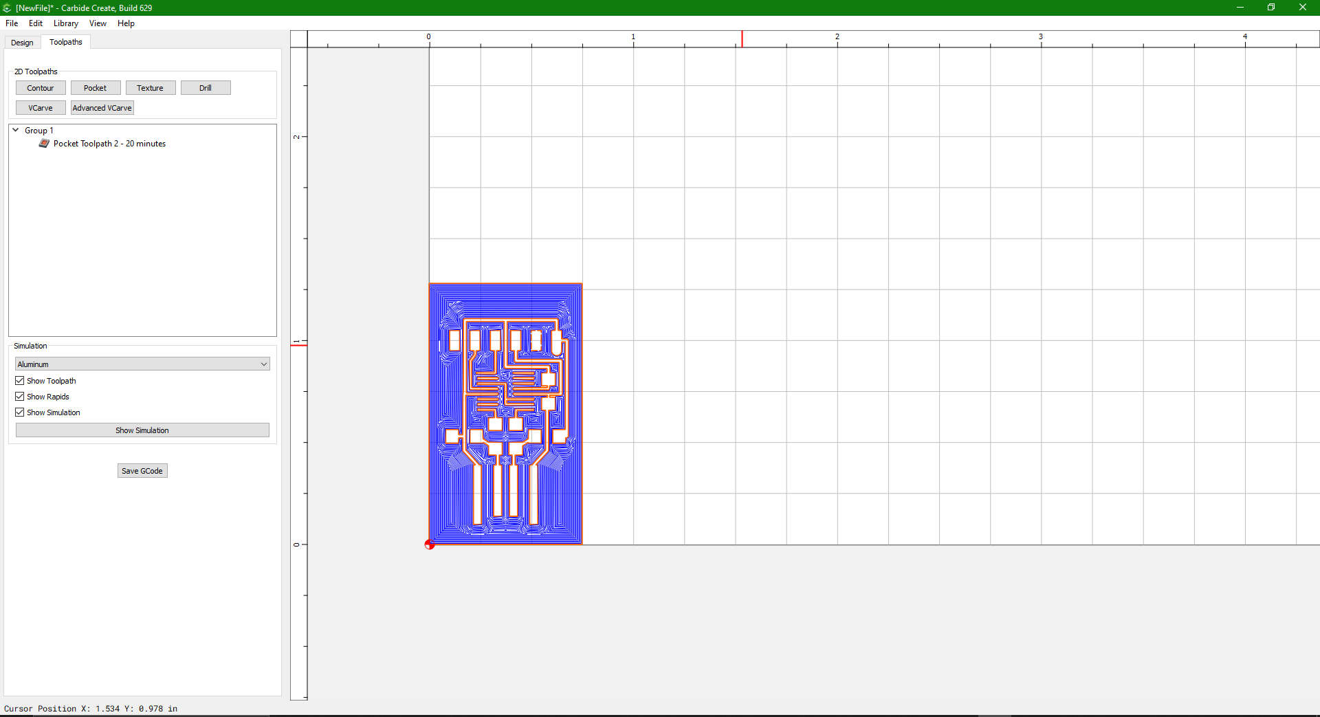
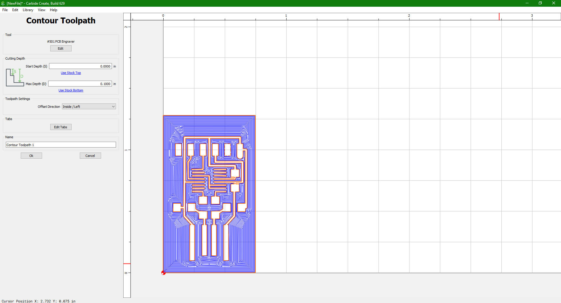
The process of MILLING the board remained very similar, with small variations, which was applied mainly to the contour and pocket settings. The very same precision mill was used, The NOMAD 3, and the ideal pocket and contour toolpath settings (seen in the images below) were used to achieve the desired outcome. Two new tools were used for the milling process, a 1/64 diameter with a 1/32 LOC (Pocketing) and a NOMAD #122 Squarecut (contouring). Also, it is worth mentioning that a UPDI board was also milled, using the same method used for the FTDI, above. The UPDI is essential for communicating the board via the FTDI cable.
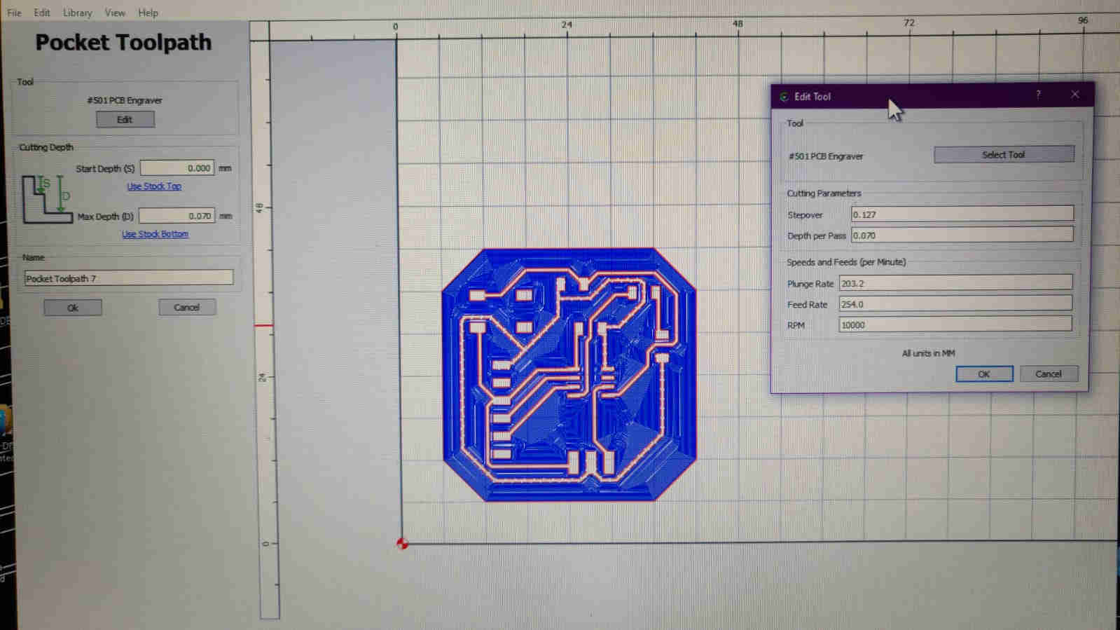
Pocket Toolpath
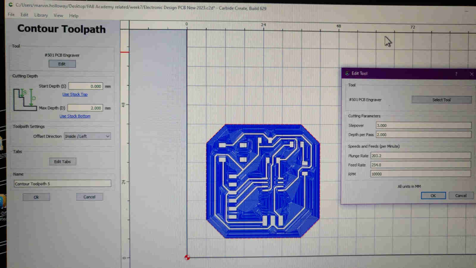
Contour Toolpath
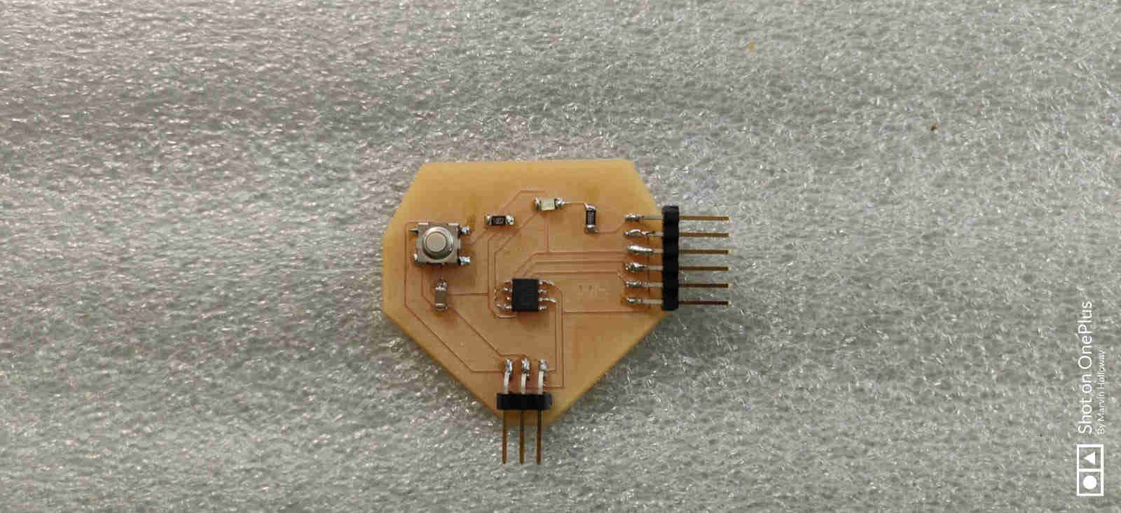
Once I was satisfied with the finished milled PCB, I proceeded to solder my components to them. In both PCB’s, the same components were used. These were:
- ATTiny 412 microcontroller (2)
- Resistor 1 Kilo ohm (x4)
- Capacitor (unpolarised) 1 Microfarad (x2)
- Tactile Switch (x2)
- LED (Blue/RED) (one of each)
Soldering
Undfortunately, the video of myself soldering the 2 aforementioned boards were corrupted, and therefore unusable, however, heres a very short video illustrating some of my soldering skills, on another board.
These were the end result, the completed PCB’s (see images below). All PCB’s were tested for continuity, conductivity, etc.
Testing
To perform a test on one these boards, I utilised the Arduino IDE software. I typed a simple sketch/ code to instruct the LED on the PCB to light when the switch was pressed.
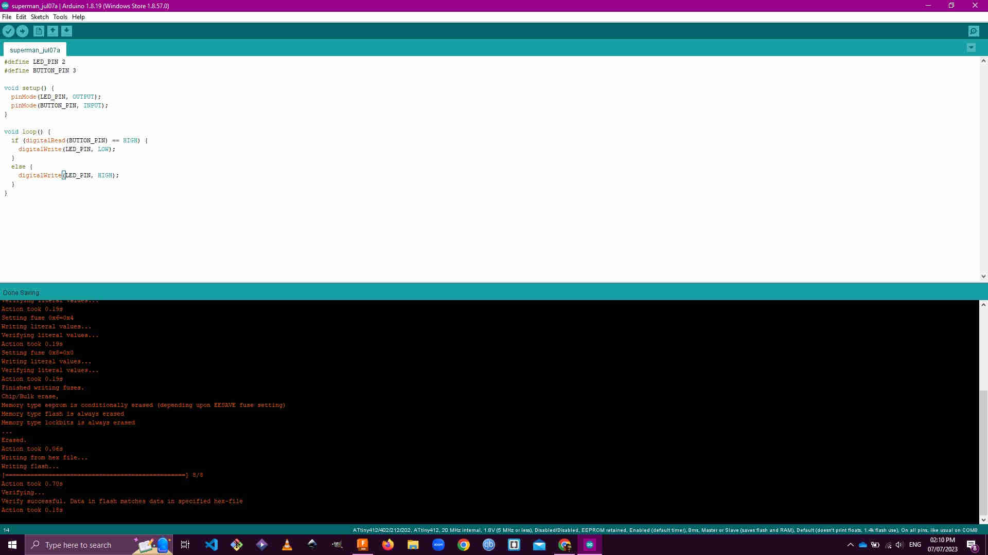
#define LED_PIN 2
#define BUTTON_PIN 3

void setup() {
  pinMode(LED_PIN, OUTPUT);
  pinMode(BUTTON_PIN, INPUT);
}

void loop() {
  if (digitalRead(BUTTON_PIN) == HIGH) {
    digitalWrite(LED_PIN, LOW);
  }
  else {
    digitalWrite(LED_PIN, HIGH);
  }
}
Success!It works! (Click on the Watch on YouTube Option)