6. Electronics design
This week I worked on defining my final project idea and started to getting used to the documentation process. - The assignment for this week was to redraw an echo hello-world board, add (at least) a button and LED (with current-limiting resistor) check the design rules, make it, and test that it can communicate extra credit: simulate its operation
Group Project
Individual Assignment
“For this weeks assignment, I decided to redesign my board to fit the microcontroller using the ATTiny 412 ssf. I took inspirations from Sophia Vona project tutorial. This was my first time designing a PCB, so it posed many challenges for me. Mostly, that of unfamiliar territory with rergards to the software. Thankfully enough, there were tutorials from past students within the Fab Academy to aid in this.
Designing the PCB
For my design, I utilised the EAGLE Software. After aimlessly trying to learn tutorials for this software, I realised that Dr. Neil Gershenfeld indicated in a previous class that Autodesk merged the Eagle software, with that of Fusion 360 😂 . It took some time to get used to the Fusion Electronics interface, as well as to add the Fab library, which was key in designing my board, but here is my progrees thus far:
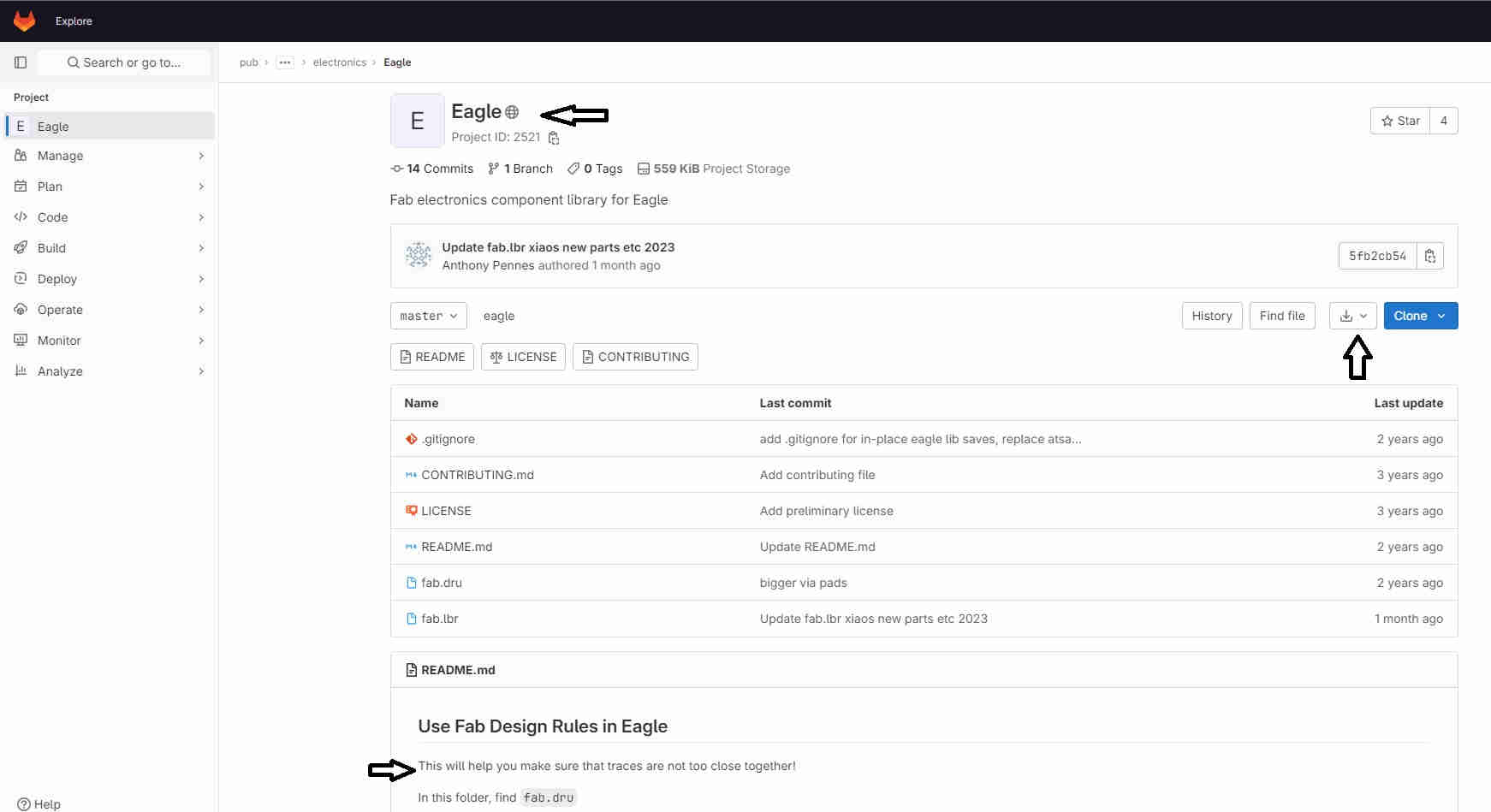
To add the FAB Library, I visited this link Fab Library, and selected the eagle as it pertained to the software app I was using. Next, I downloaded the fab.lbr file from the git hub, as seen in the images below.
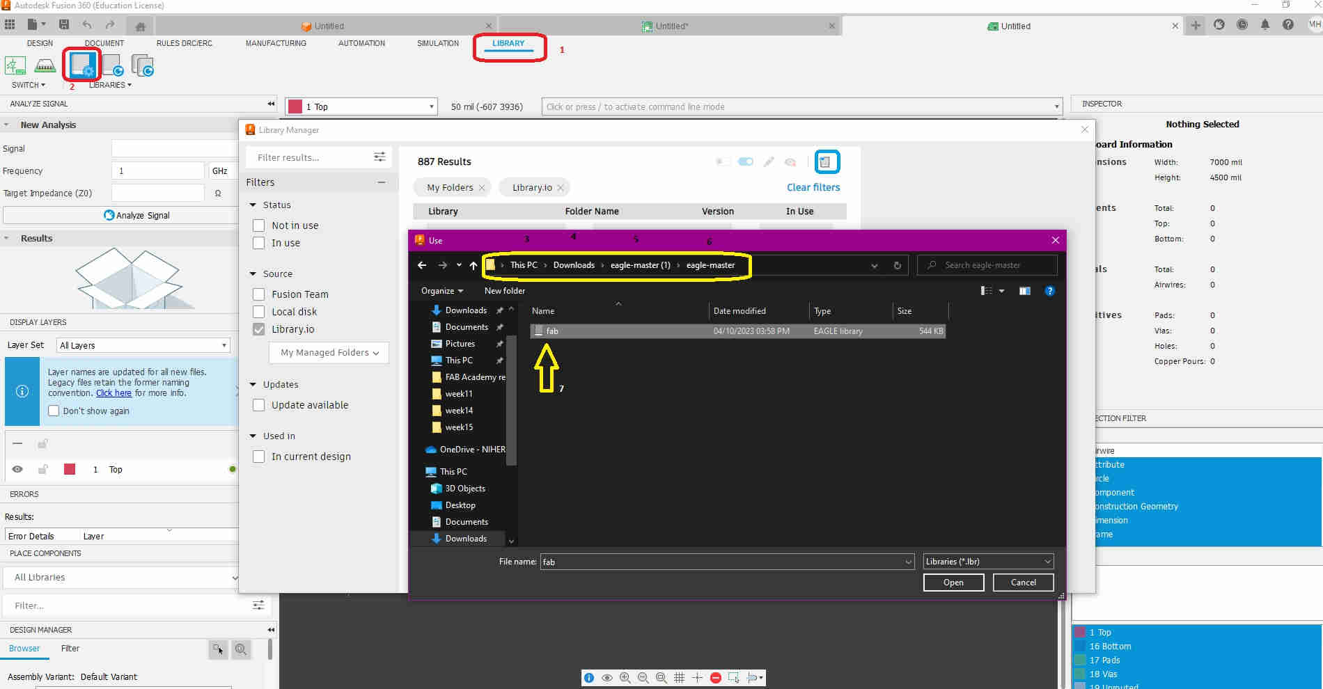
After this was done, I proceeded to integrate/ add the Fab Library to Fusion 360. To accomplish this, I took the steps as seen below, within the image below, as follows;
In Fusion - Go to Library Tab - Open Library Manager - Import Library - Choose from Local Disk (as it’s already downloaded) - Choose and locate the respective download folder the library file was downloaded to (usually the “Downloads” folder) - Once file is located, click open - Voila! the fab library has been added to your Fusion 360 app
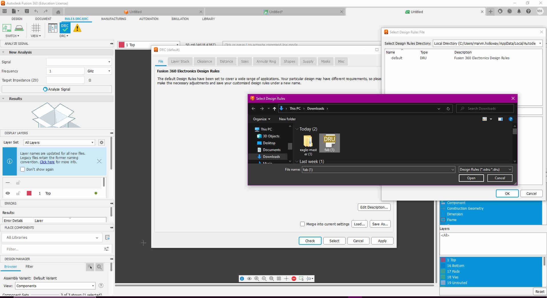
Next on the agenda, was to set up the DRC (Design rules check)/ERC(Electroncis rules check). This was done to standardise my designs so that it meets Fab Academny standards, as well as, ensure that I don’t run into any errors when designing my PCB.
To achieve this, I utilised the same link I used to aquire the Fab library earlier, and downloaded the fab.drc file off of git hub’s Fab academy Repository. From there, I then had to add/ import the file to the DRC. This procedure can be seen in the consequetive images seen below;
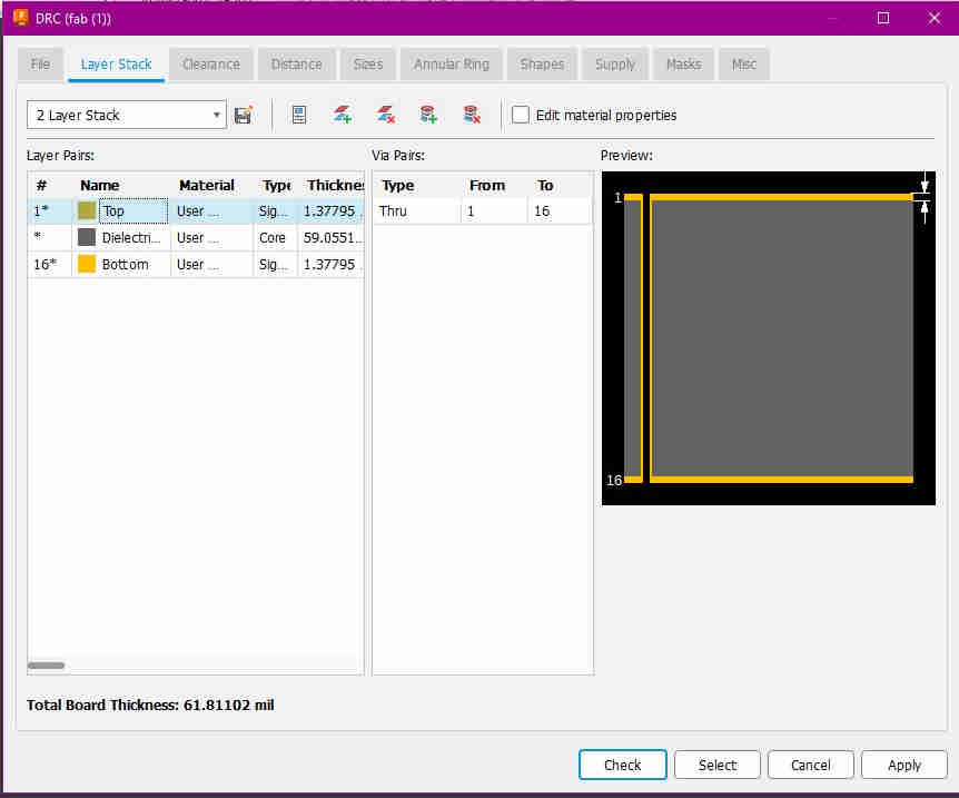
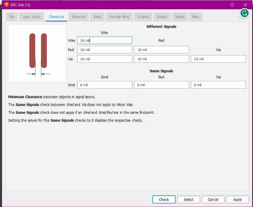
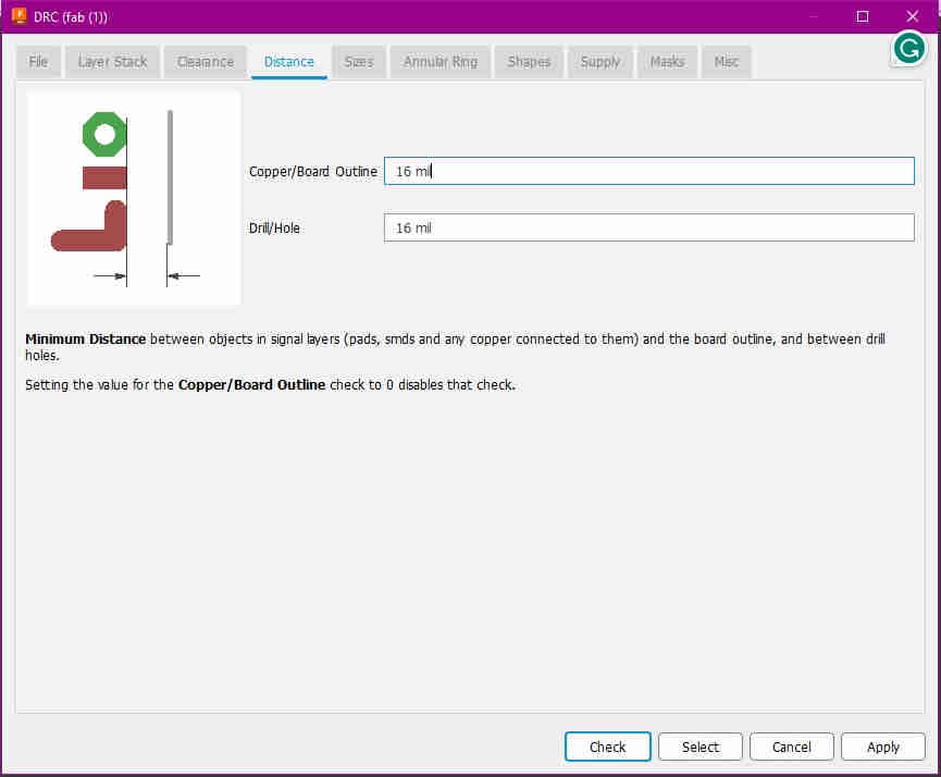

I left most of the settings in thier default state, for the remainder of tabs not showned here in detail, as recommended by Fab academy, however, I did change the thickness (width) of my traces/ lines, from 10 mil, to 16 mil, as seen in the image above.
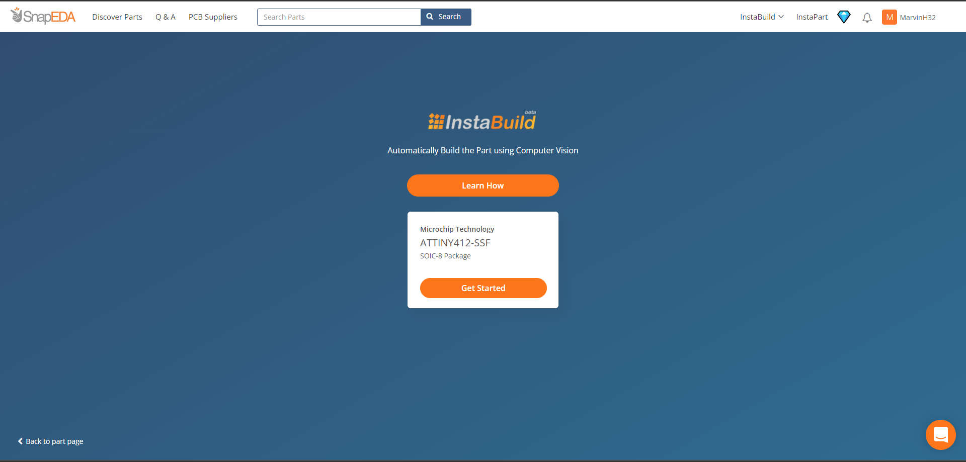
Some of the components couldn’t be located within the Fab library, at the time, so I was informed by a collegue that I will have to manually build one. the component in question is none other than the ATTiny 412 ssf. This webpage came in very handy in this process, SnapEDA.
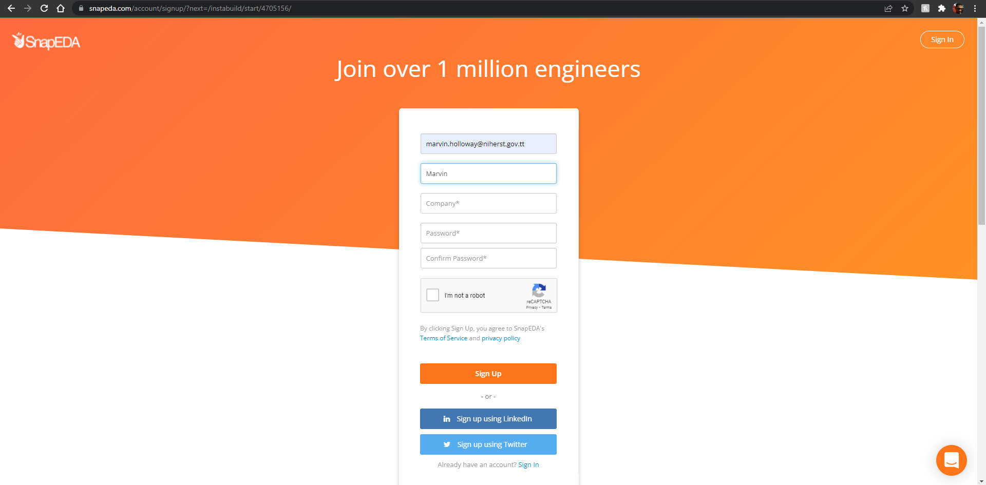
As expected, these websites do require registration first
Once that was done, I did a search for the part
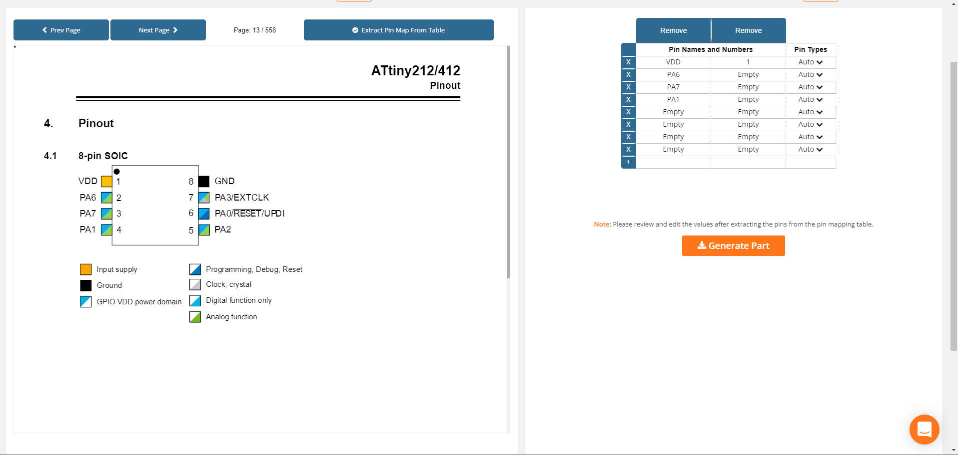
Then I began mapping the correct pin orientation, as it would be relfected within my pcb
With this done, I then proceeded to download my footprint, and add it to the component library within fusion
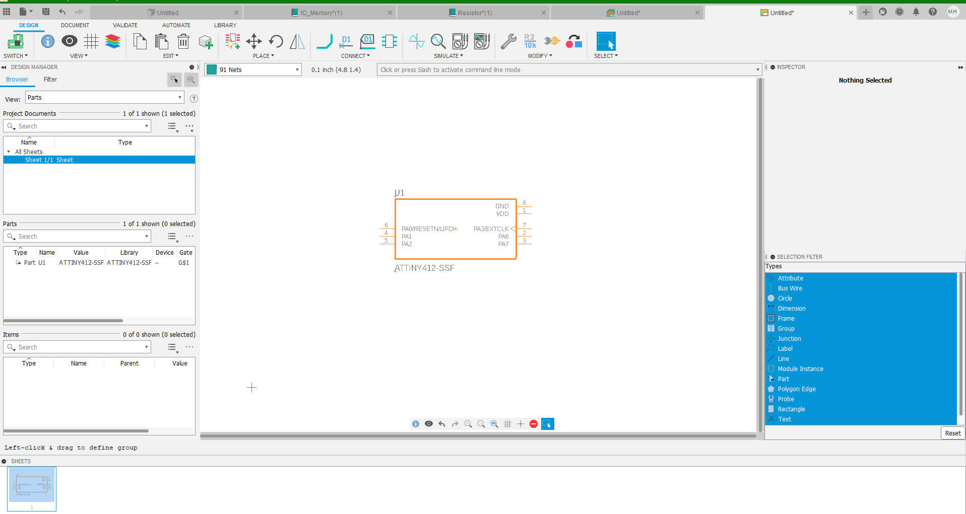

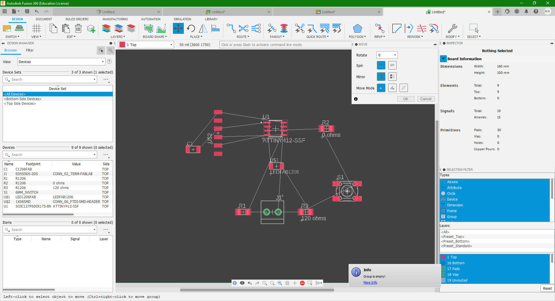
Using fusion electronics design/ eagle integrated, I began creating my schematic, I placed my IC first, then proceeded with the other components, from the fab library
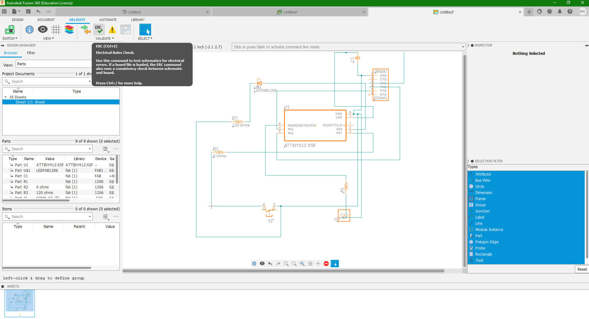
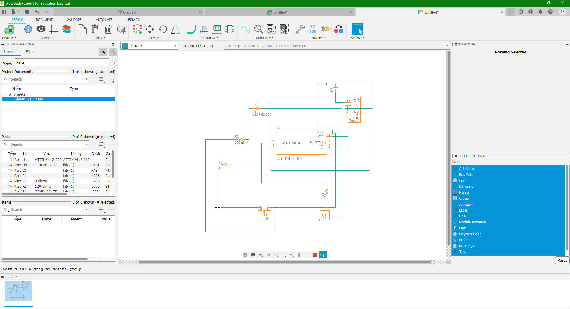
I then wired my components to each other, and then did an ERC (Electronics Rules Check). This is done to test the schematic for any electrical errors.
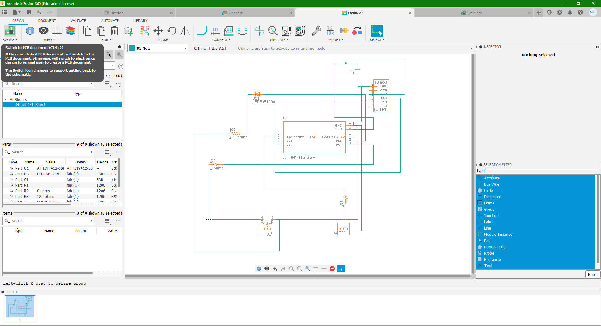
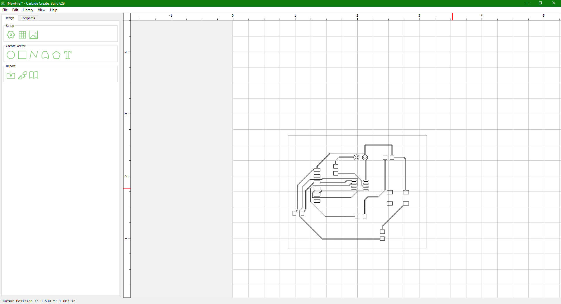
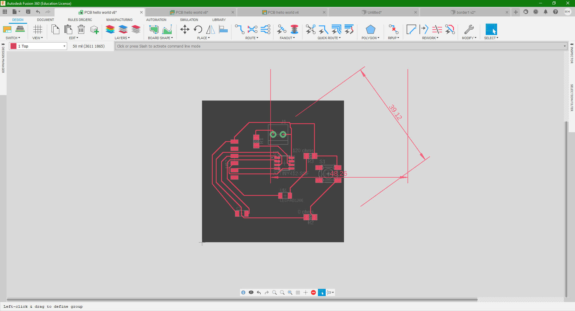
With that done, I then switched to my schematic to a PCB document. Within this workspace, I am able to percieve my components more naturally, and route my wires/ traces more practically.
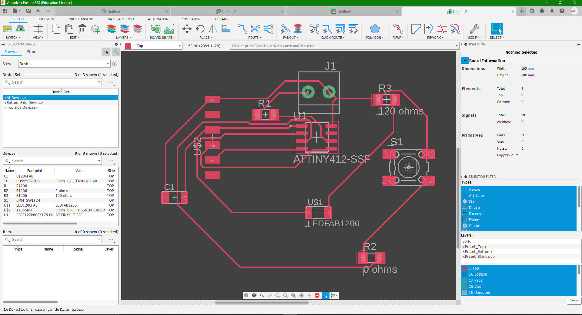
At first I decided to reroute my PCB to clean up the “RatsNest” of wires manually, one by one, to make my pcb appear more uniformed and neat
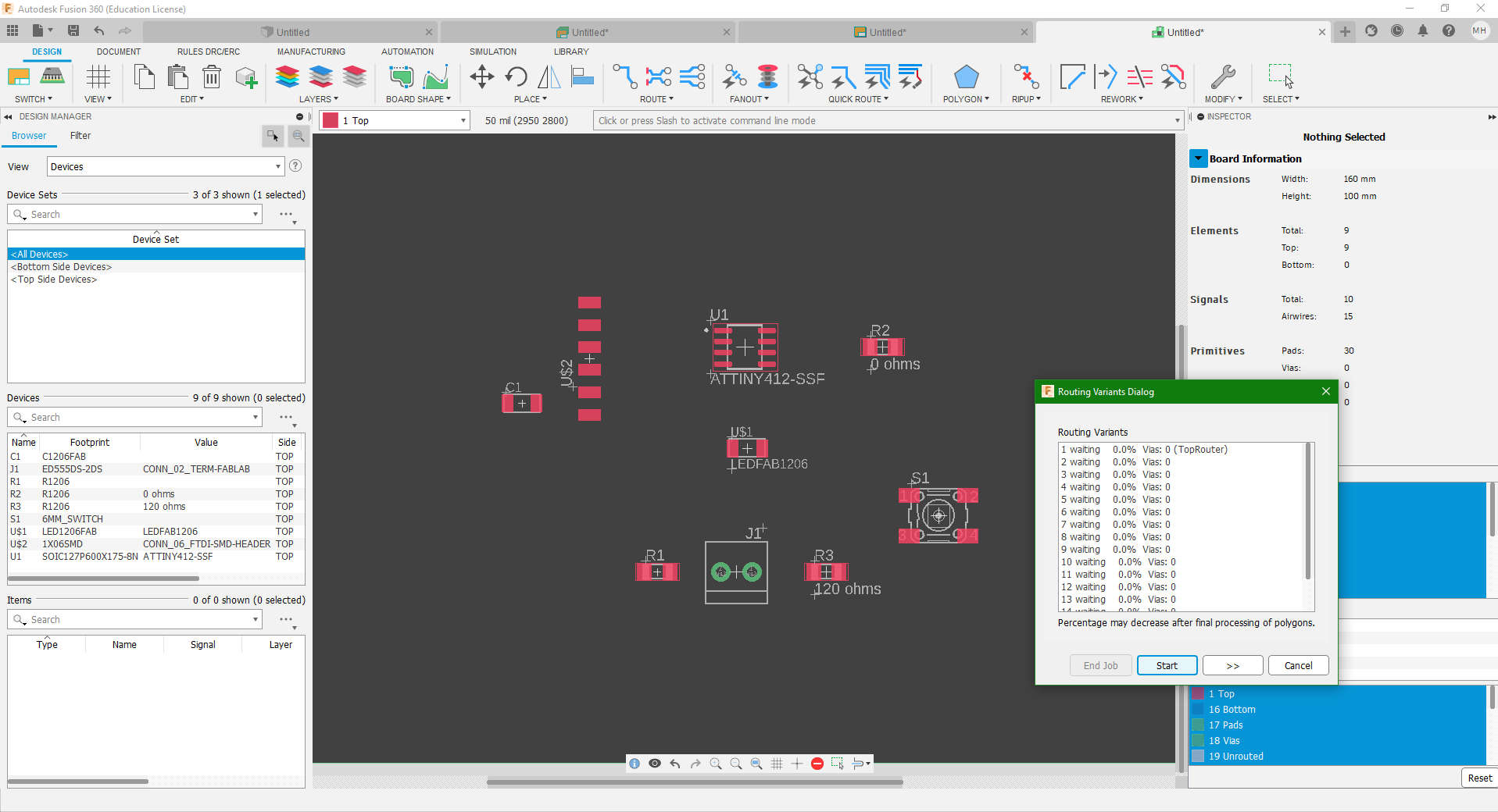
Only to realise that there was an option to do this operation, automatically (Quickroute)

Upon completion of this, I did some minor/ major edits till I accomplished an design I was content with


I then selected the manufacturing preview to export my design in a format ready for milling
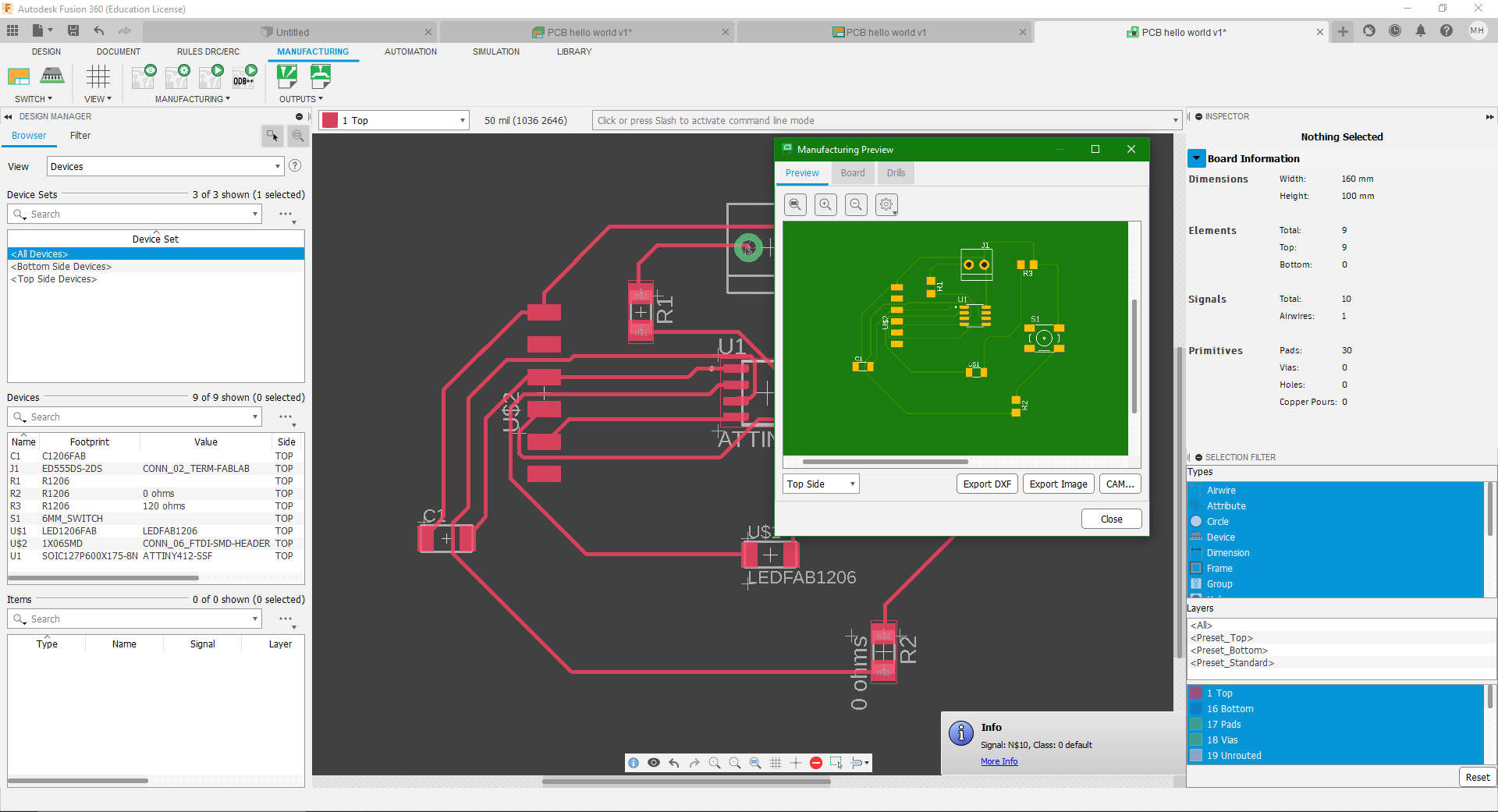
PCB file found here Hello world
Milling the PCB
To mill my PCB, I utilised the Desktop CNC Milling machine, The Nomad 3 Pro. Both Carbide Create and Carbide Motion are the interfaces used to further edit and actually run the milling job. More of the setting up process as well as the file covnersion neccesary to detect the boards’ traces, essesntially the conductive material that is left on the copper circuit board, can be found here Electronics production
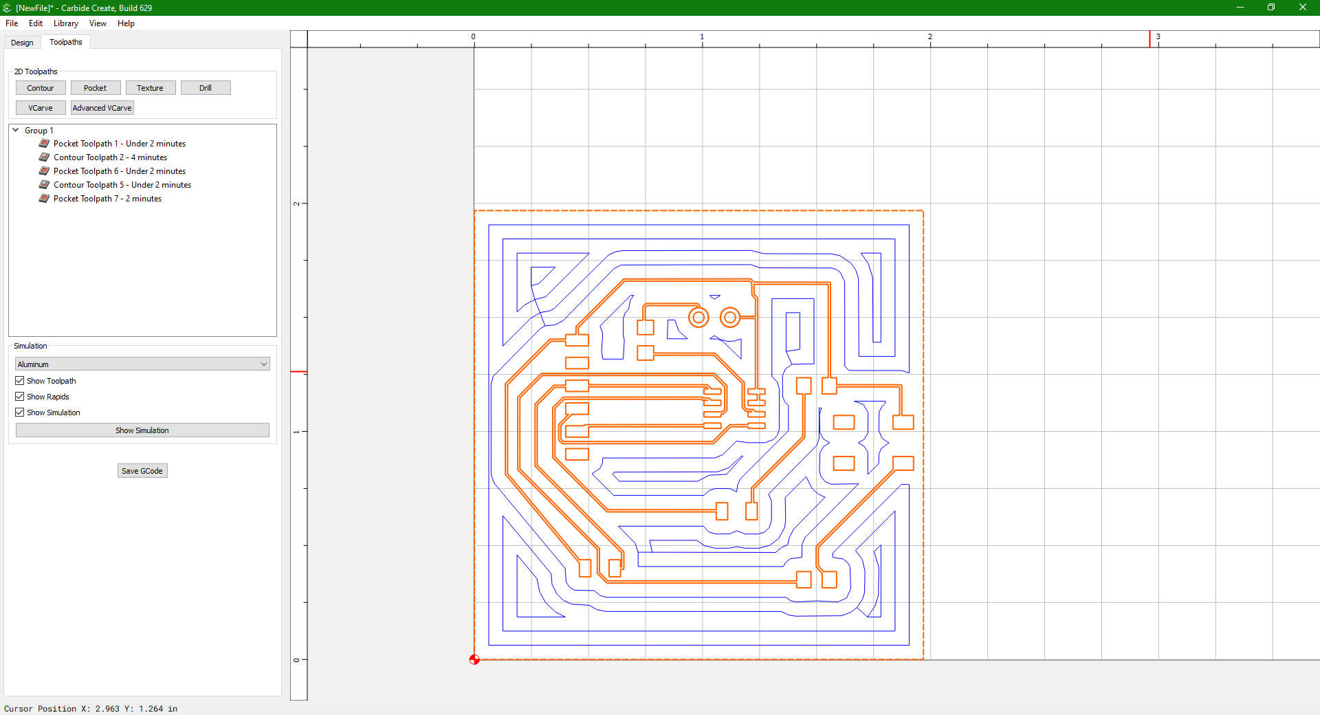
Importing the dxf file to carbide create was relatively straight forward
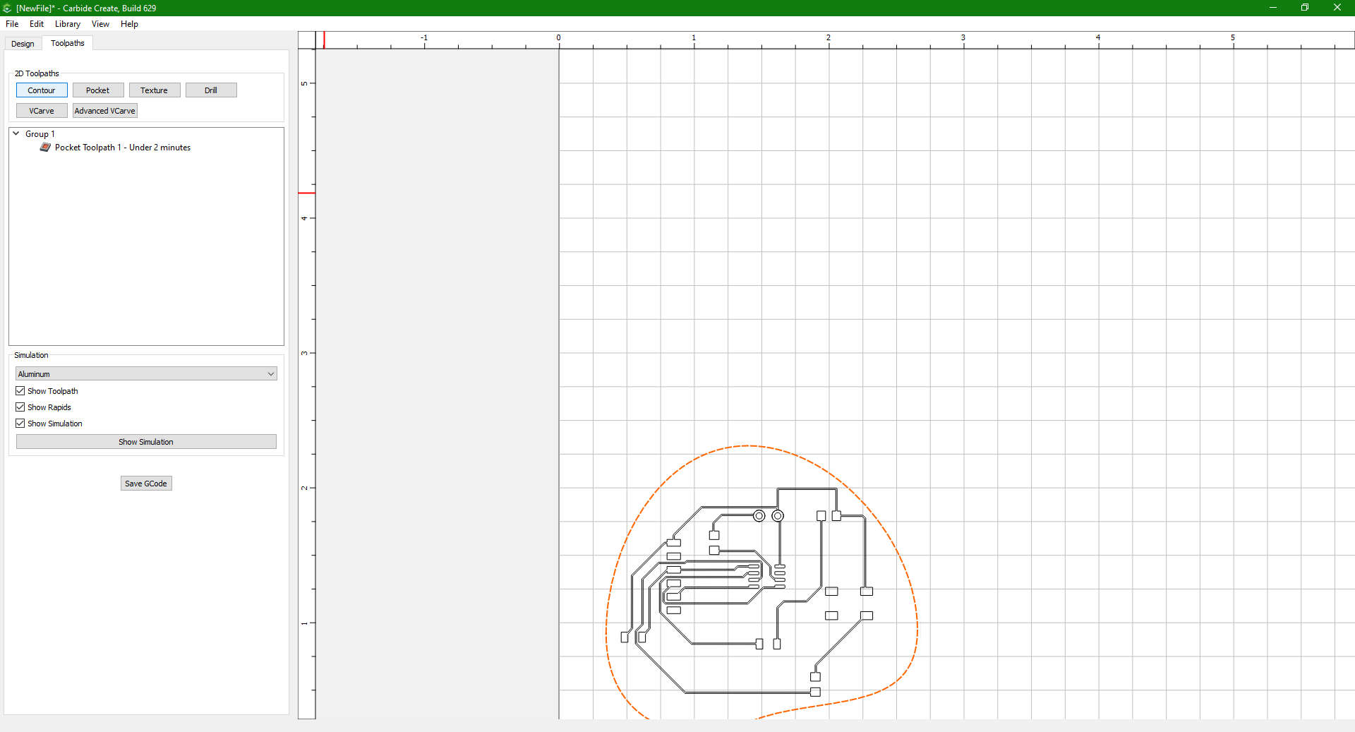
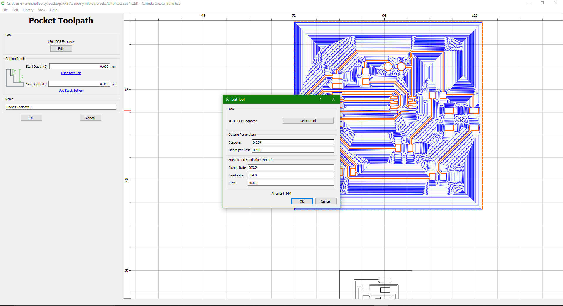
Then I set my pocket toolpath (the path the milling tool takes to “engrave” the copper material thereby leaving the traces for soldering). Determining the neccesary parameters for milling
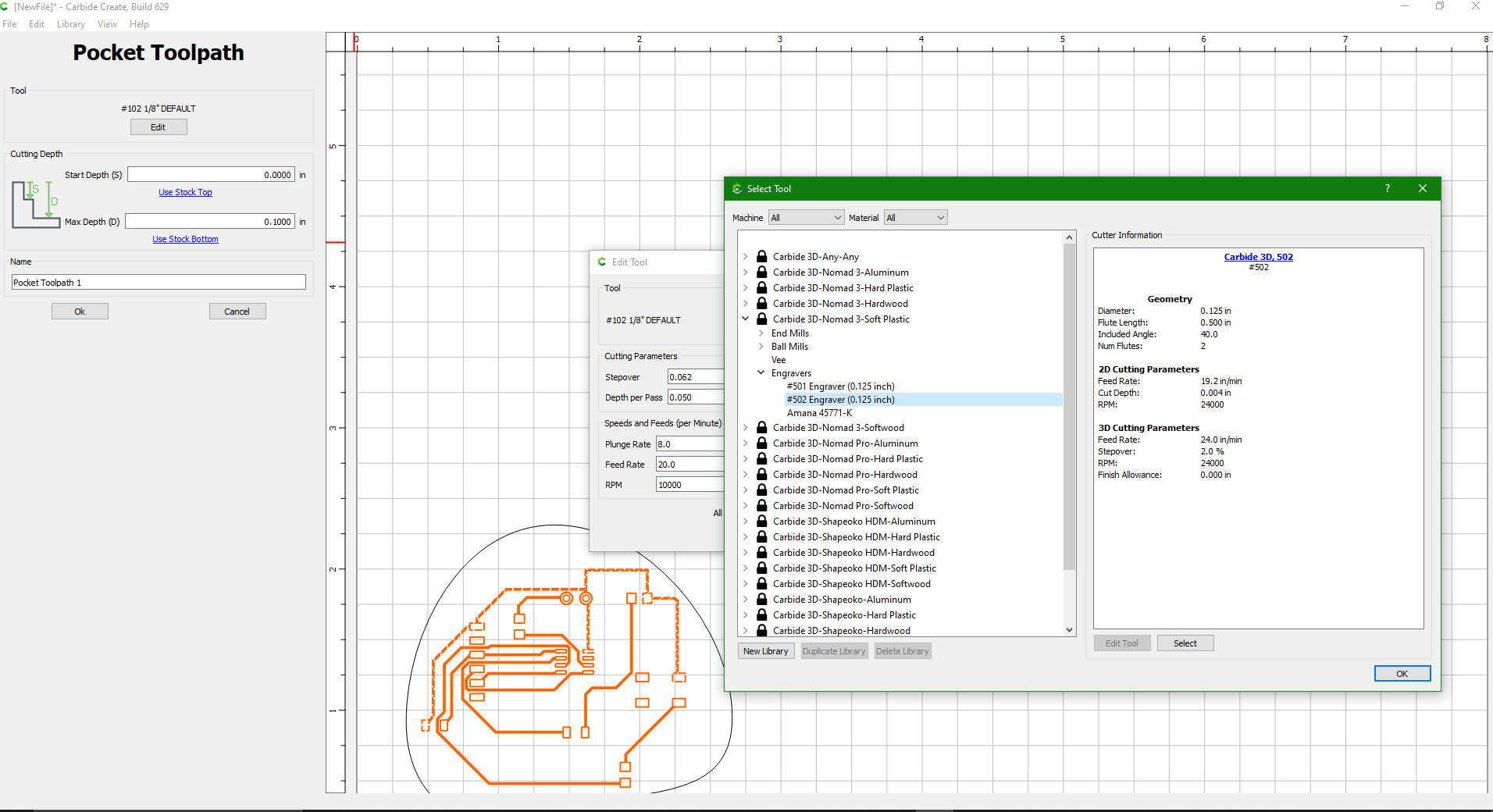
After that, I set my contour toolpath (the path the milling tool takes to “fully cut” the copper material, ergo, the border). I realised that I hadn’t properly created a border for my PCB and played around with some of the more unconventional shapes within carbide create.
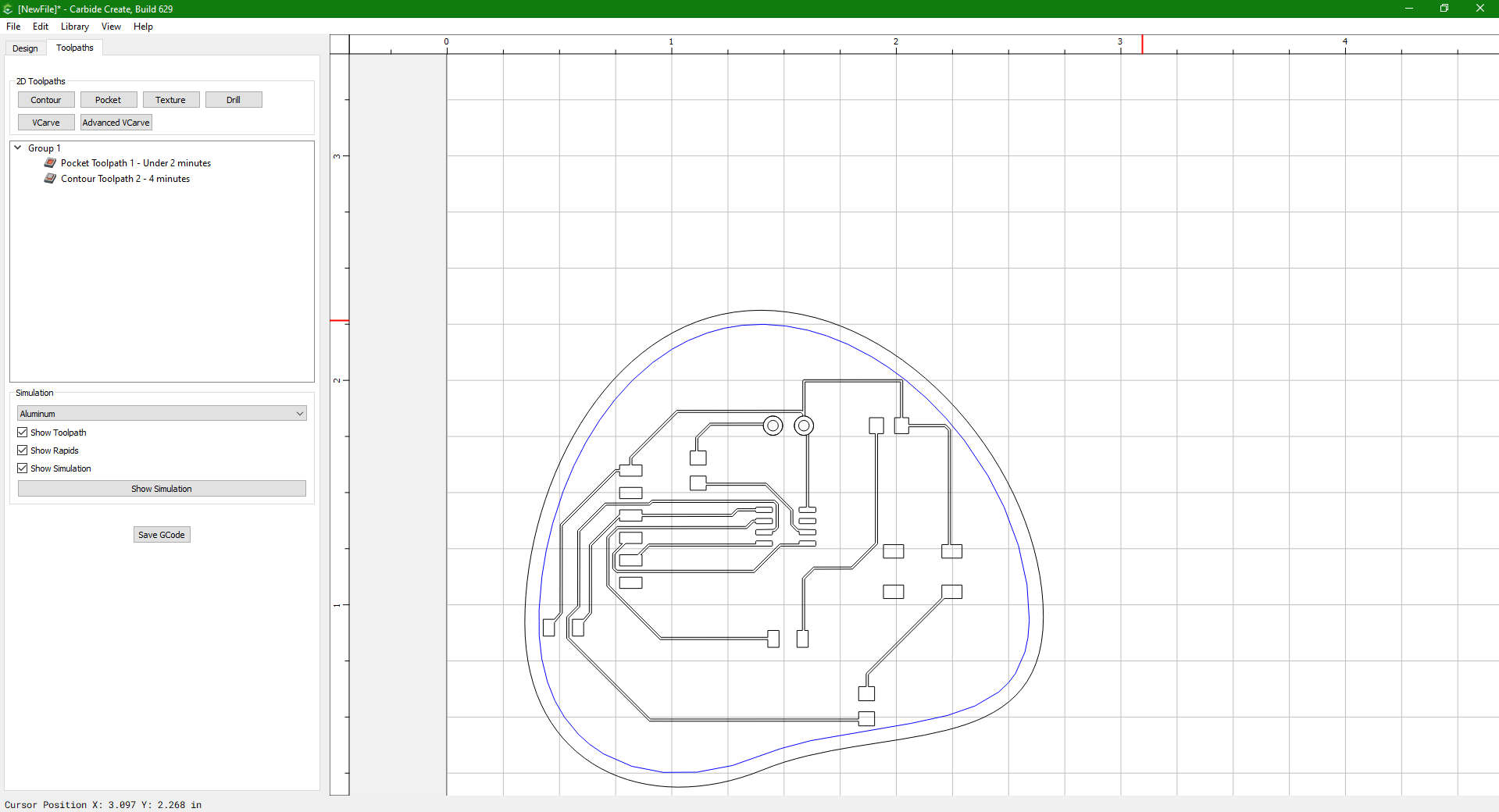
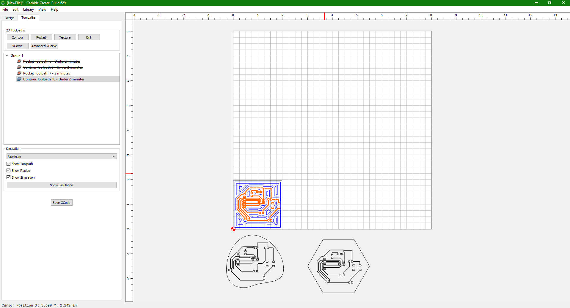
Not satisfied with my border, I went back to fusion360 and created one there instead
Then I reimported the file and repeat the process of setting the parameters for the toolpaths
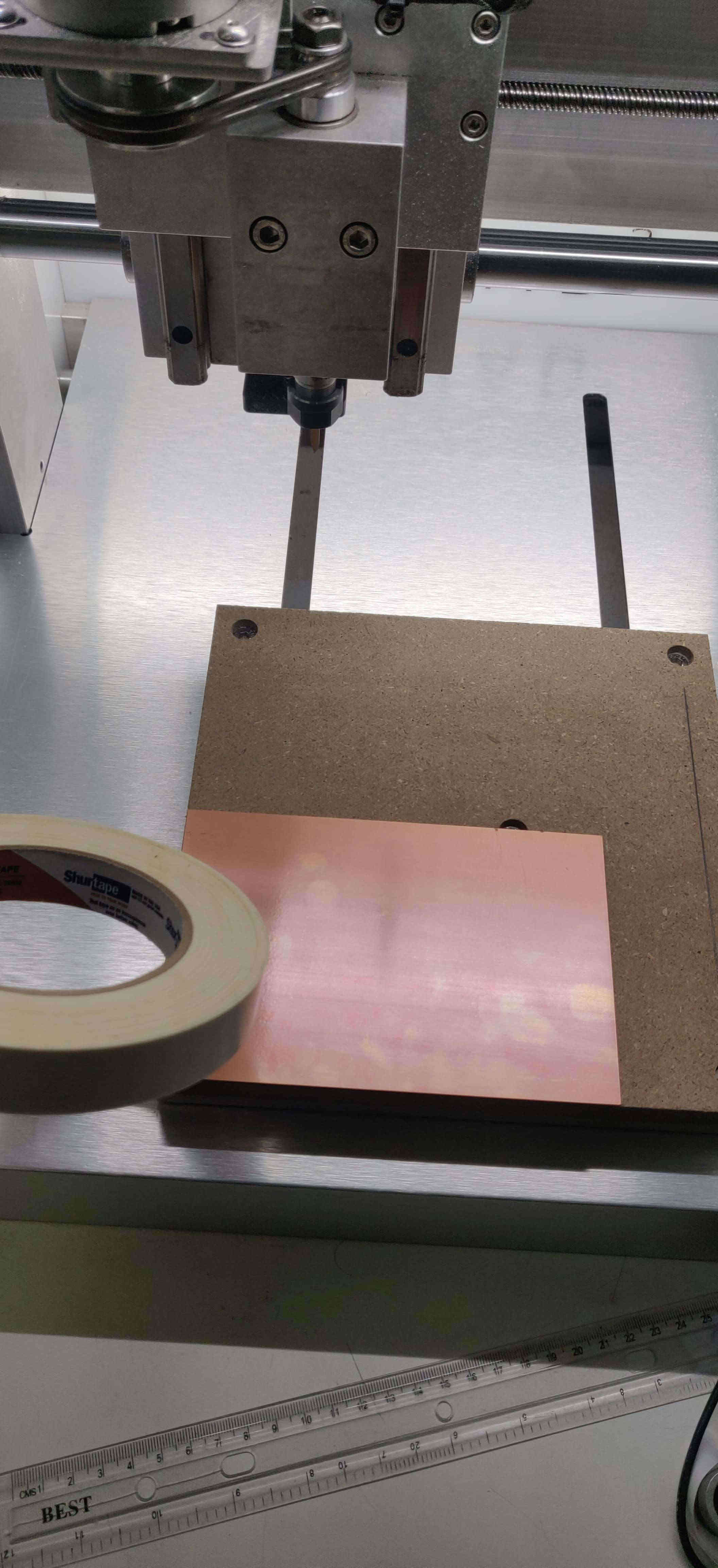
I connected my laptop to the Nomad 3, and opened the carbide motion interface. Jogged the milling head to ensure accurate probing, then set the probing tool in place and initiated the probing process.
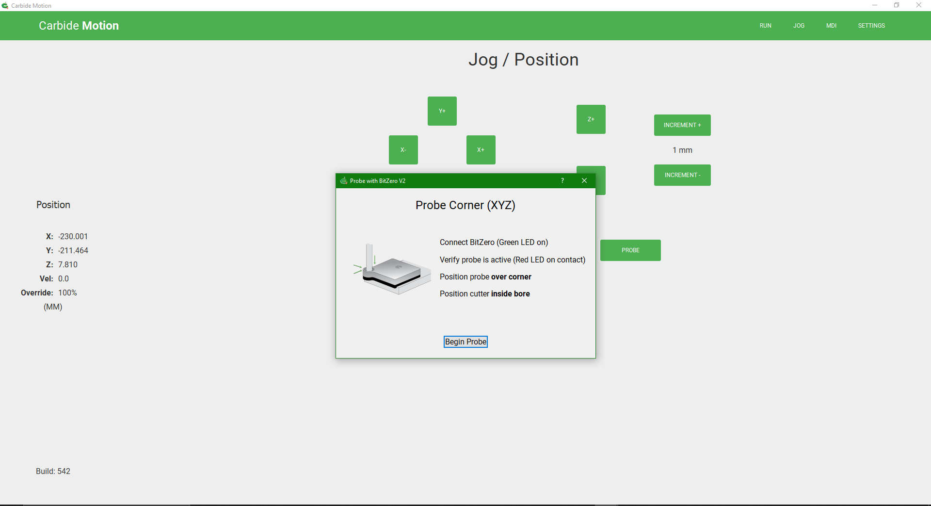
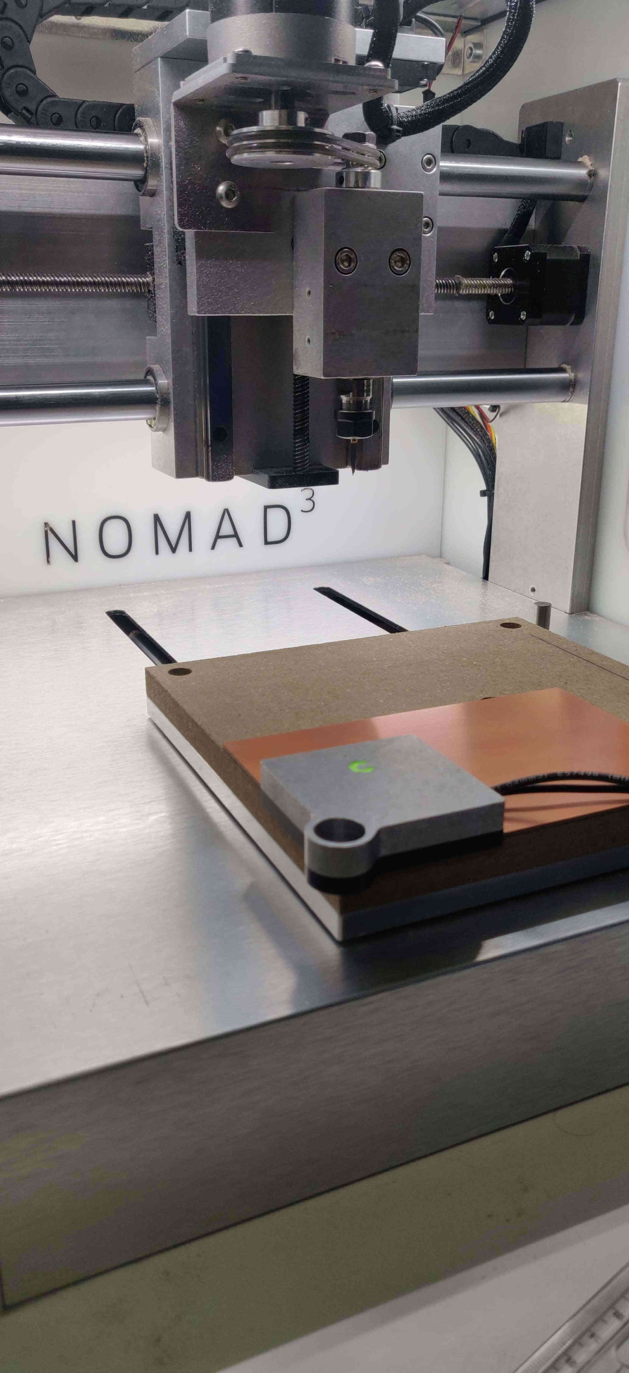
I obviously stuck my board in place with the strong 2 sided adhesive packaged with the Nomad 3
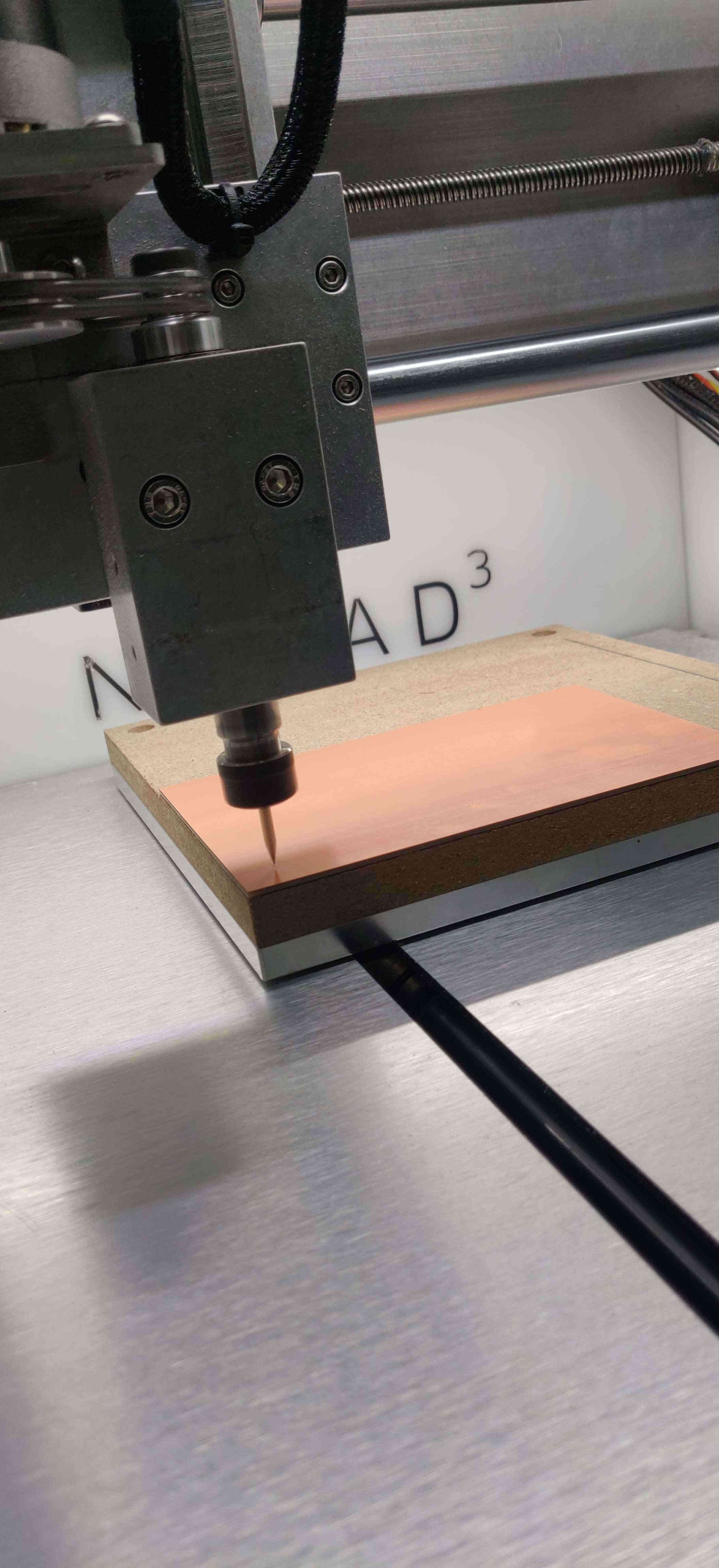
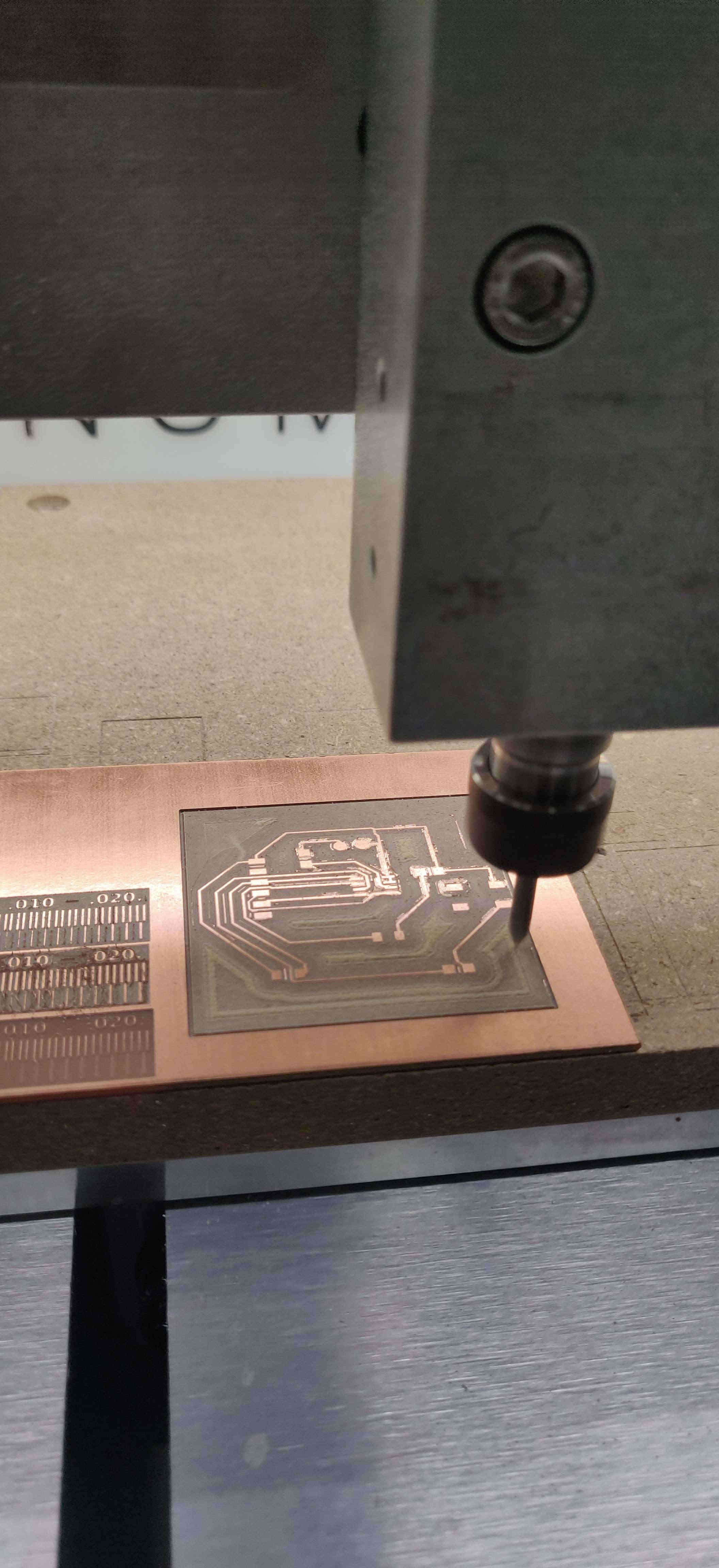
Finally, I began the milling of the board
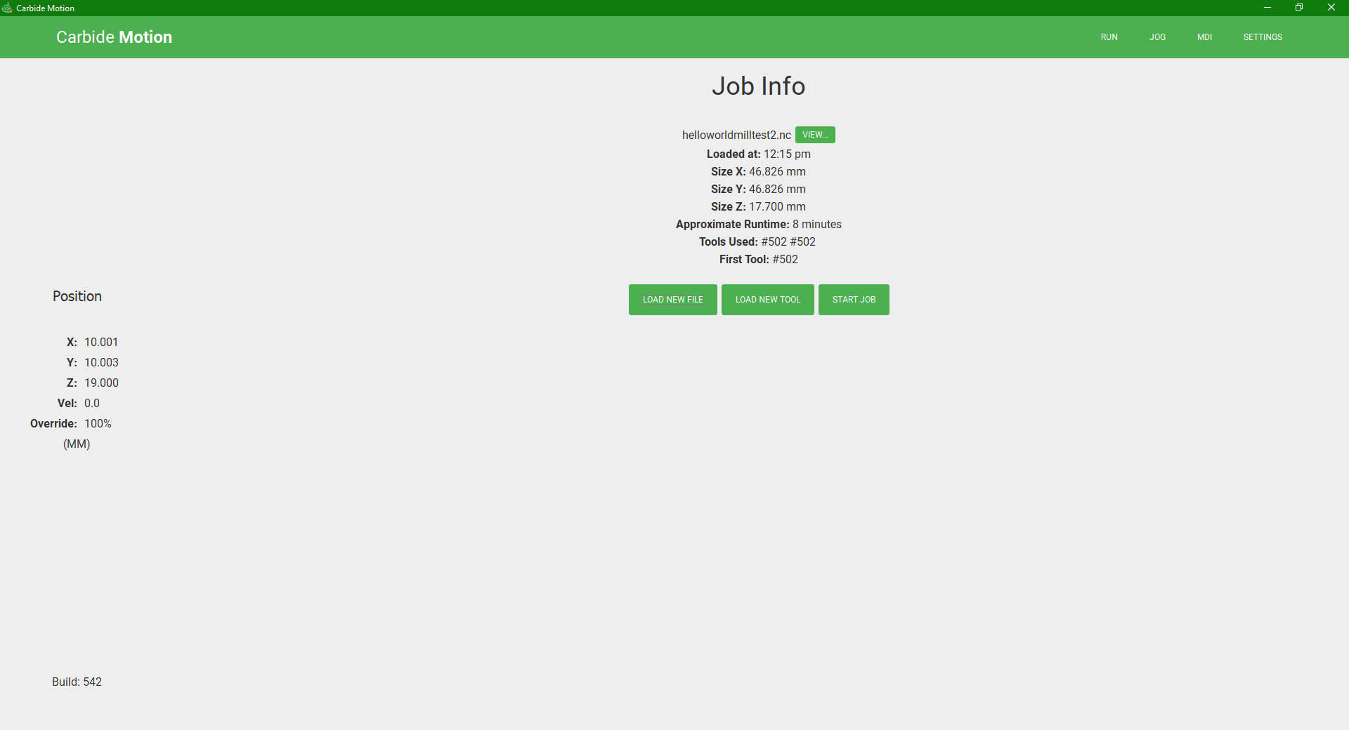
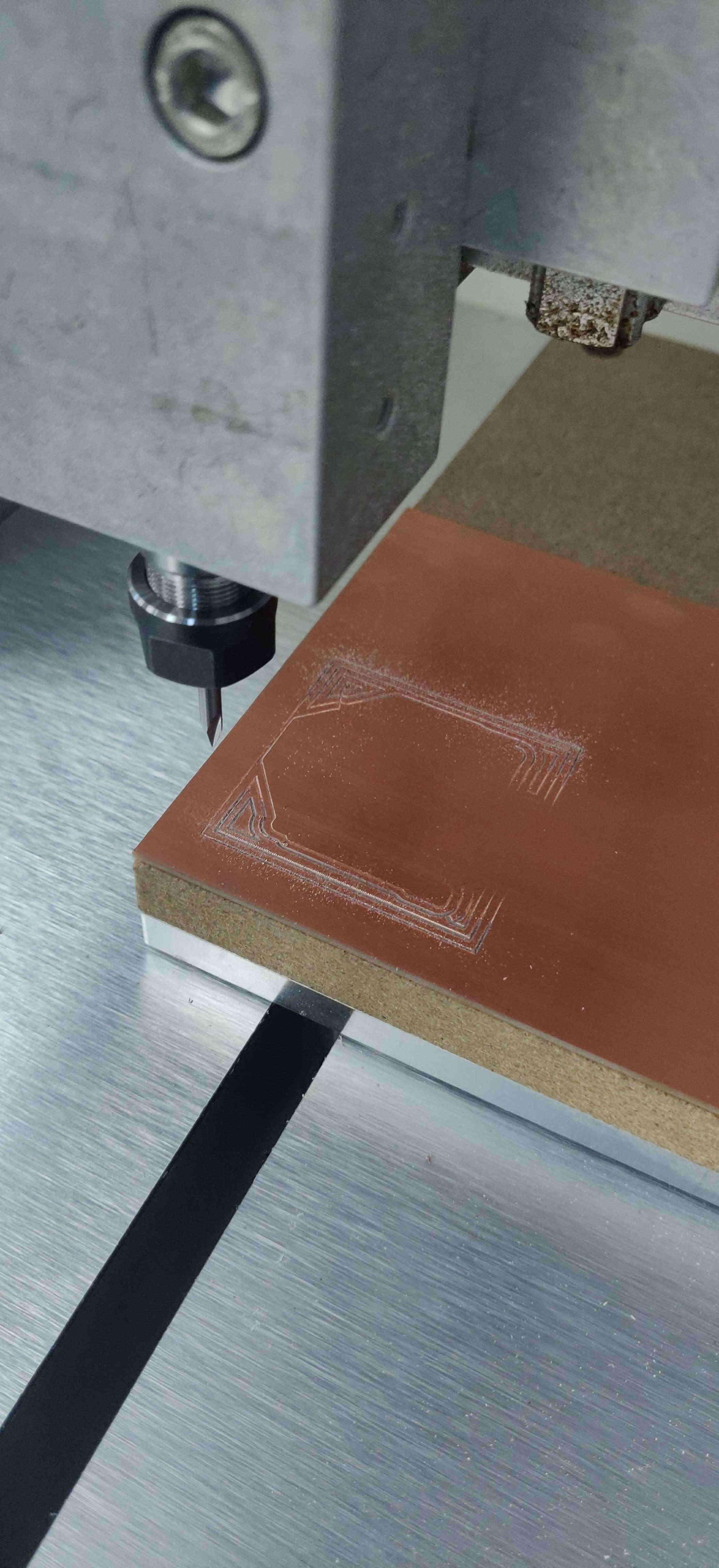
Unfortuantely, the tool did not reach the depth required to mill both the pocket and contour toolpaths, so at this point I spent hours using “trial and error”, adjusting the cutting tools depth ever so slightly to mill my board. To be cont’d.
Useful Links/Apps
Update!
As mentioned in Week4 (Electronics Production), a Nomad 3 Milling Machine Collet, was sourced, purchased and installed, enabling me to produce my UPDI board. Determining the cutting parameters were of course, very tricky, challenging and time consuming when it came to milling my design for this weeks assignment. As I initially used inches as my overall unit of measure for my Carbide Create, I decided that millimetres may provide a more precise measurement for the parameters. I also observed that many physical factors may have interfered with the operation of the milling quality. Such as; how flush the PCB board is relative to the wasteboard on the Nomad, the thickness of the adhesive material meant to keep the material (PCB) in place, any type of sediment that may hamper/ interfere with the cutting operation.
Once those concerns were remedied, cutting my design became alot more managable. Something worth noting is that, as a precaution of any software errors, as I have experienced during this process, it is important to take a screenshot image of your working parameters (as you would see below), this can be used as a backup in the case the file either gets corrupted or doesn’t save properly.
[Carbide Cut file with GCode]Carbide Test cut 5.c2d
Here are the cutting parameters I used that worked for me

Here are some failed attempts
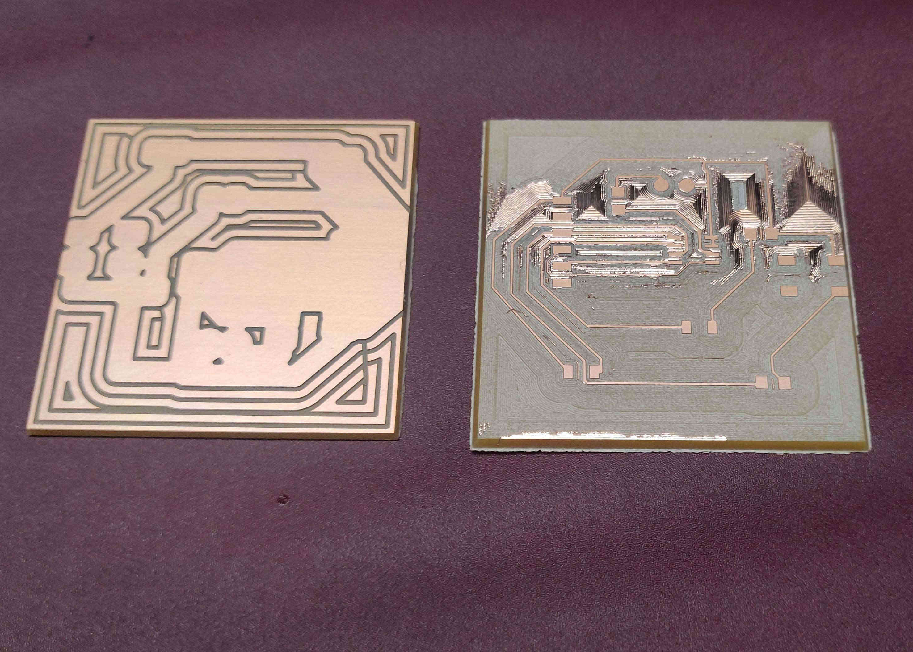
Final Milling and the Milled PCB prior to soldering, As you can see closely, there is still material needed to be milled away

Soldering
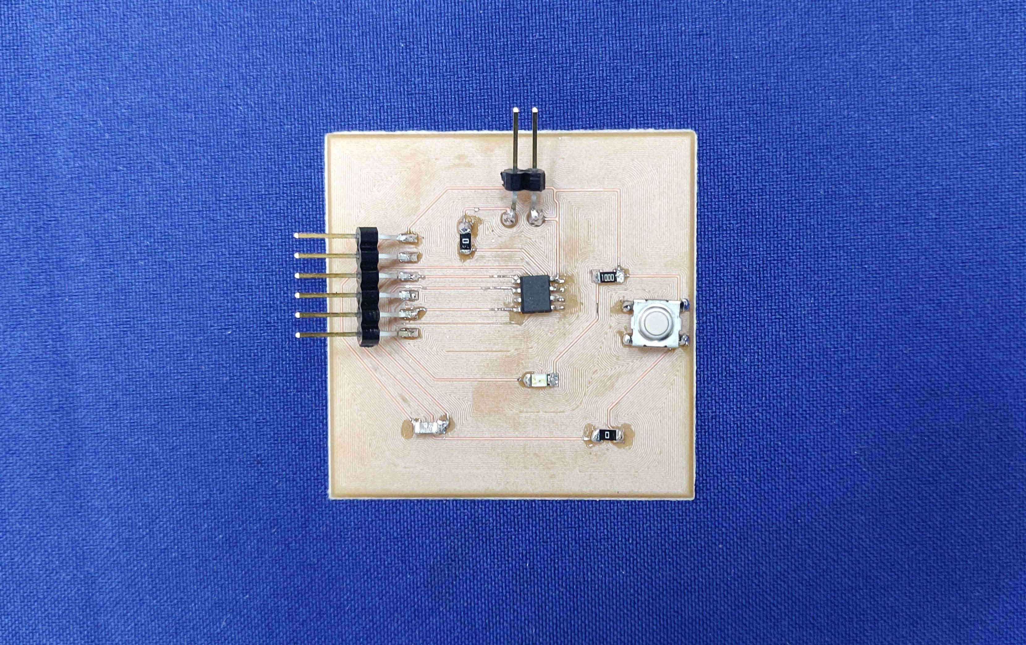
For the soldering aspect of my PCB, I found it a bit challenging, which seems to be a common reaccuring theme at this point. This was noted especially for the ATTiny 412 SSF IC. The pins were so minute, that soldering between them were a pain. With an entire Sunday evening and great patience, dedicated to getting the job done, I got the components soldered in place. Hopefully without damage to said components. I must credit one of my groups members Ravi Baldeo who came up with an ingenious way to keep the PCB in place, thereby limiting human error, (seen below)

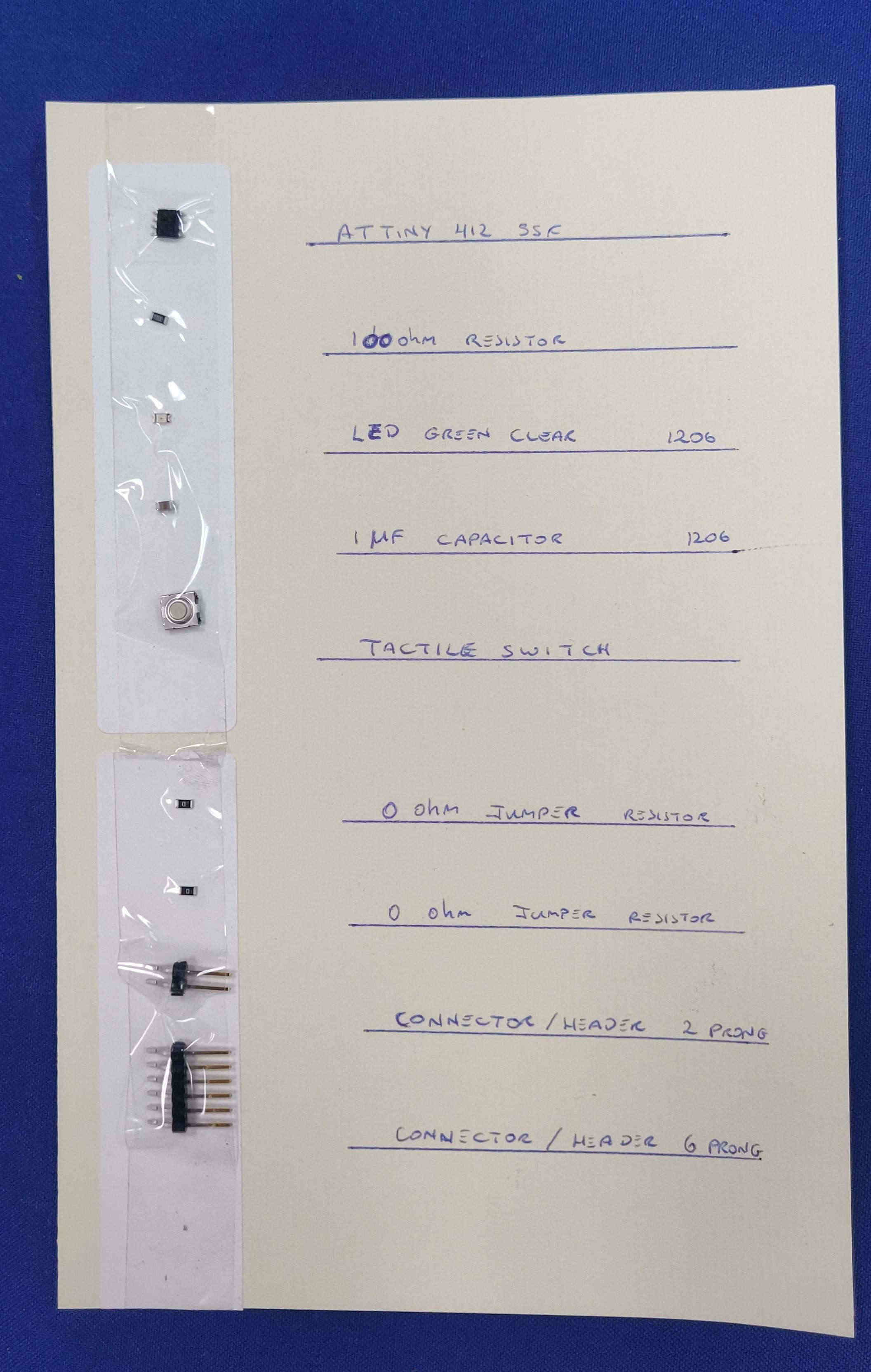
Component list, so as to provide easy access for soldering (NOTE: Ensure you are grounded when handling the ATTiny 412)
Final Product