7. Electronics design
Electronic circuit design involves ideation, creation, and revision. Learn about PCB design and the circuit design process.
Learning outcomes
-
Select and use software for circuit board design
-
Demonstrate workflows used in circuit board design
Like the previous weeks , student are expected to complete two (2) categories of weekly assignment.
-
Group assignment:
-
Use the test equipment in your lab to observe the operation of a microcontroller circuit board (in minimum, check operating voltage on the board with multimeter or voltmeter and use oscilloscope to check noise of operating voltage and interpret a data signal)
-
Document your work to the group work page and reflect on your individual page what you learned
-
-
Individual assignment:
- Redraw one of the echo hello-world boards or something equivalent, add (at least) a button and LED (with current-limiting resistor) or equivalent input and output, check the design rules, make it, test it. Optionally, simulate its operation.
Group Assignment
Our group assignment was to use the testing equipment in the lab to:
-
Observe the operation of the micro-controller circuit board using a multimeter
-
Use an oscilloscope to check noise of operational voltage and interpret a data signal
At the NIHERST Fablab we had access to:
The Group Assignment page is as follows Link
Group Members:
-
Nervene Bhagwandass
-
Christopher Proute
-
Terrence Carew
-
James Khan
-
Marvin Holloway
-
Ravi Baldeo
Individual Assignment
I chose the ATTINY412-echo hello world board for my Electronics design assignment .
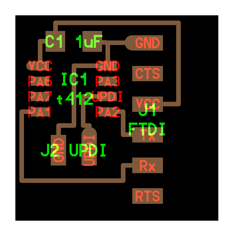
ATTiny412 The ATtiny412 is a microcontroller using the 8-bit AVR processor with a hardware multiplier, running at up to 20 MHz and 4 KB Flash, 256B SRAM and 128B of EEPROM in an 8-pin package. The series uses the latest technologies from Microchip with a flexible and low-power architecture, including an Event System and SleepWalking, accurate analog features, and advanced peripherals
-
VCC and GND is the part where you provide voltage to the chip so you provide power.
-
Green pins PA0, PA1, PA3, PA6, PA7 are programmable, but some of them have special functions - No.6 or PA0 is the UPDI programming pin. Also PA6 and PA7 are also programmable, but these are TX and RX which stands for basic serial communication. When you are going to connect an FTDI cable to it the operating system is going to establish a serial connection and through this serial connection you will be able to talk with the chip by using resending and receiving bits and bytes.

Designing the Board
I used Autodesk fusion to design my ATTINY412 echo hello-world board.
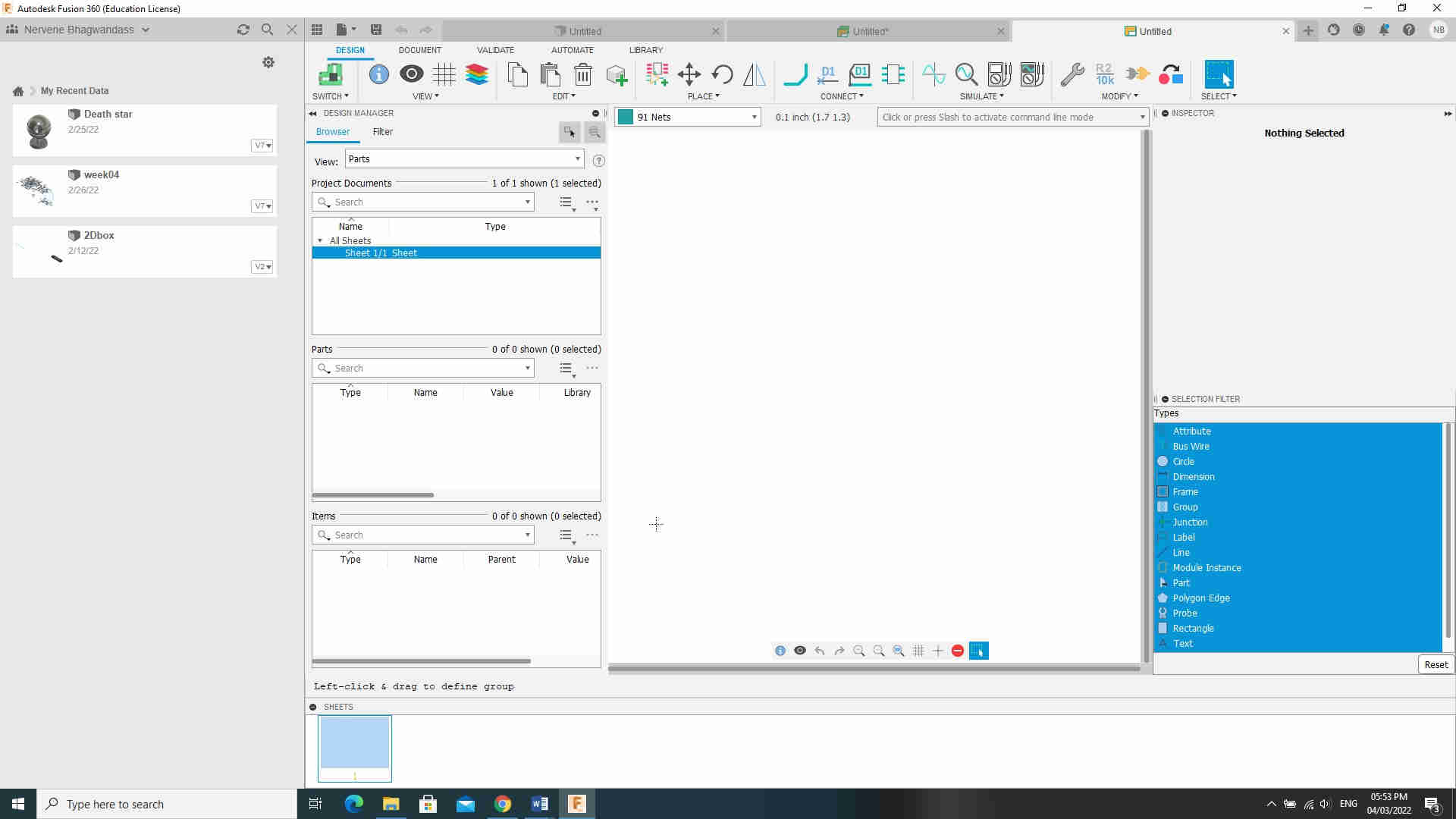
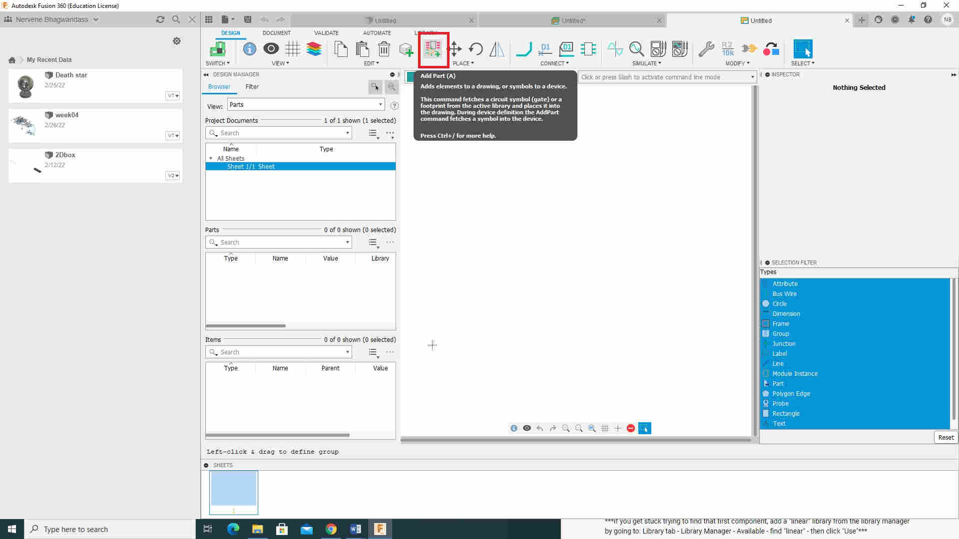
First step was to download and add following Eagle libraries to Libraries folder; Add part > Open Library Manger >> Available> Browse( and navigate the folder containing the files below)> open >Use
But in the first step, i didn’t find the main component was not on the fab.lbr list.
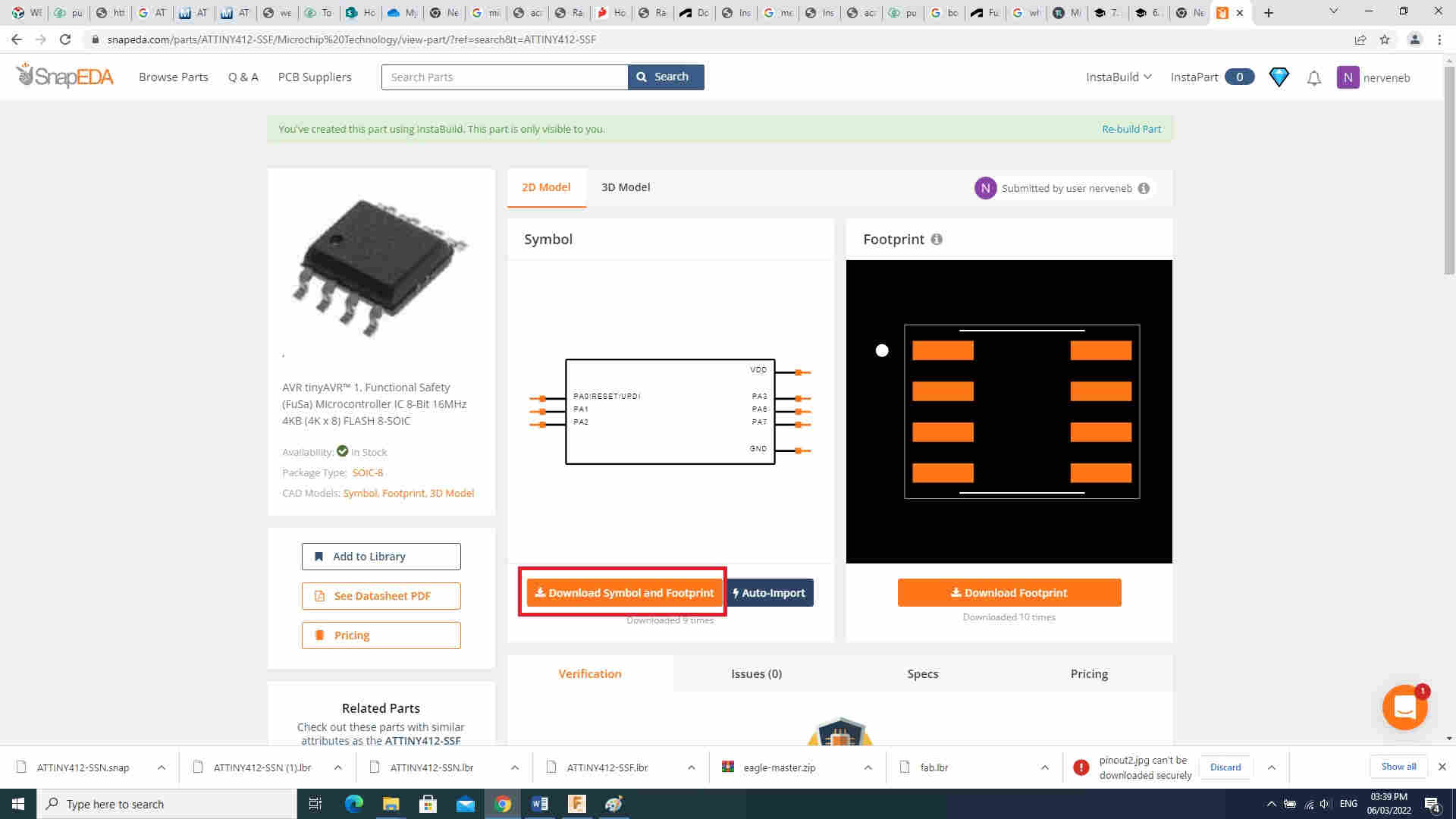
First open the snapeda page then enter keywords-attiny412

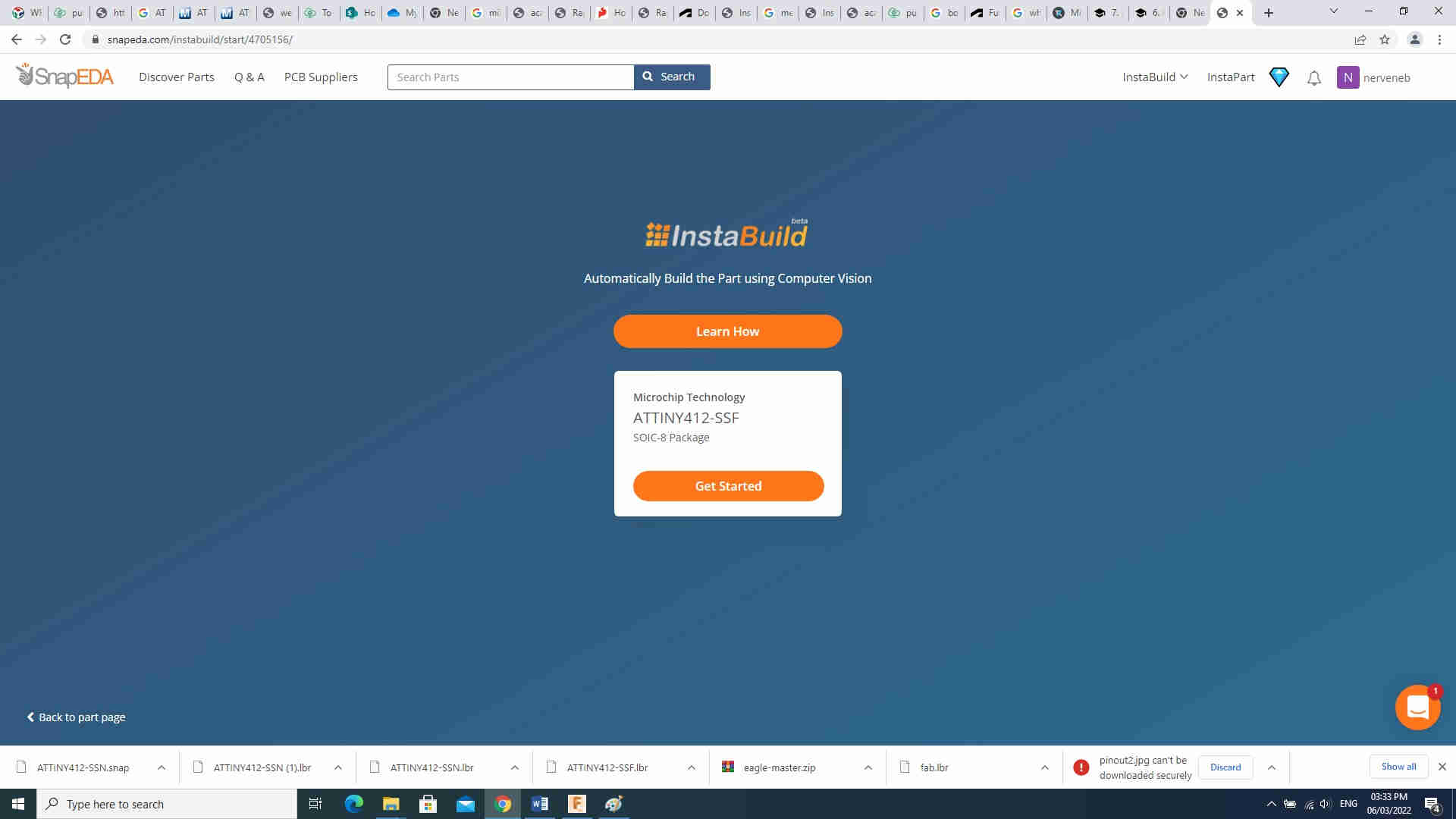
Choose ATTINY412-SSF. Second, generate the PIN names, numbers, and type, then click generate part, and download it for eagle. Third, put the new lbr file in librar


I then chose ATTINY412-echo and identify all the components/parts required for the echo hello board are:
-
ATTINY412-SSF
-
CONN_06_FTDI-SMD-HEADER
-
CAP_UNPOLARIZEDFAB
-
CONN_03SMD_RA_MALE
-
GND
-
VCC
-
LEDFAB1206
-
SW_SWITCH_TACTILE_6MM6MM
-
R1206FAB(499Ω)
-
R1206FAB(10KΩ)
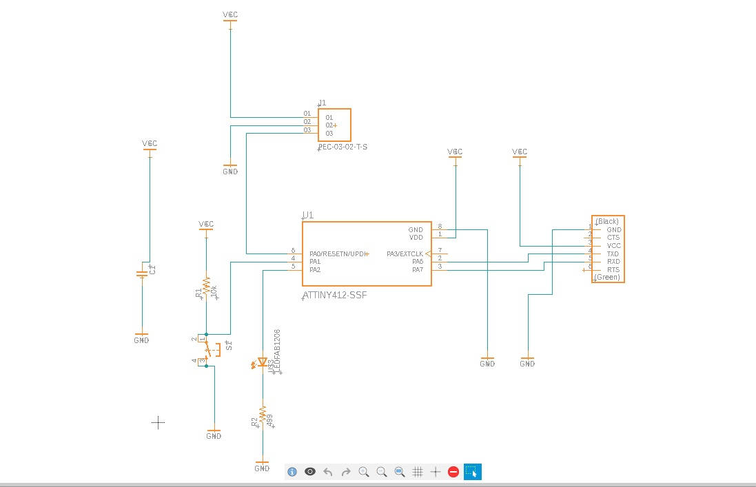
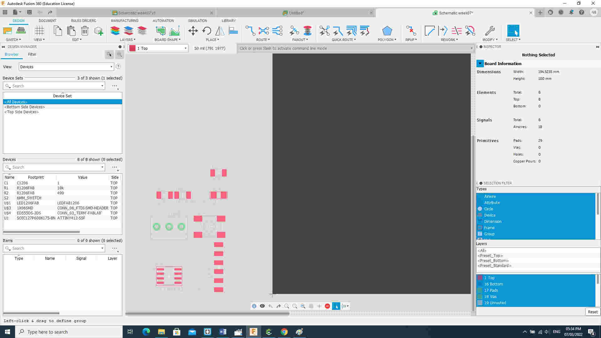
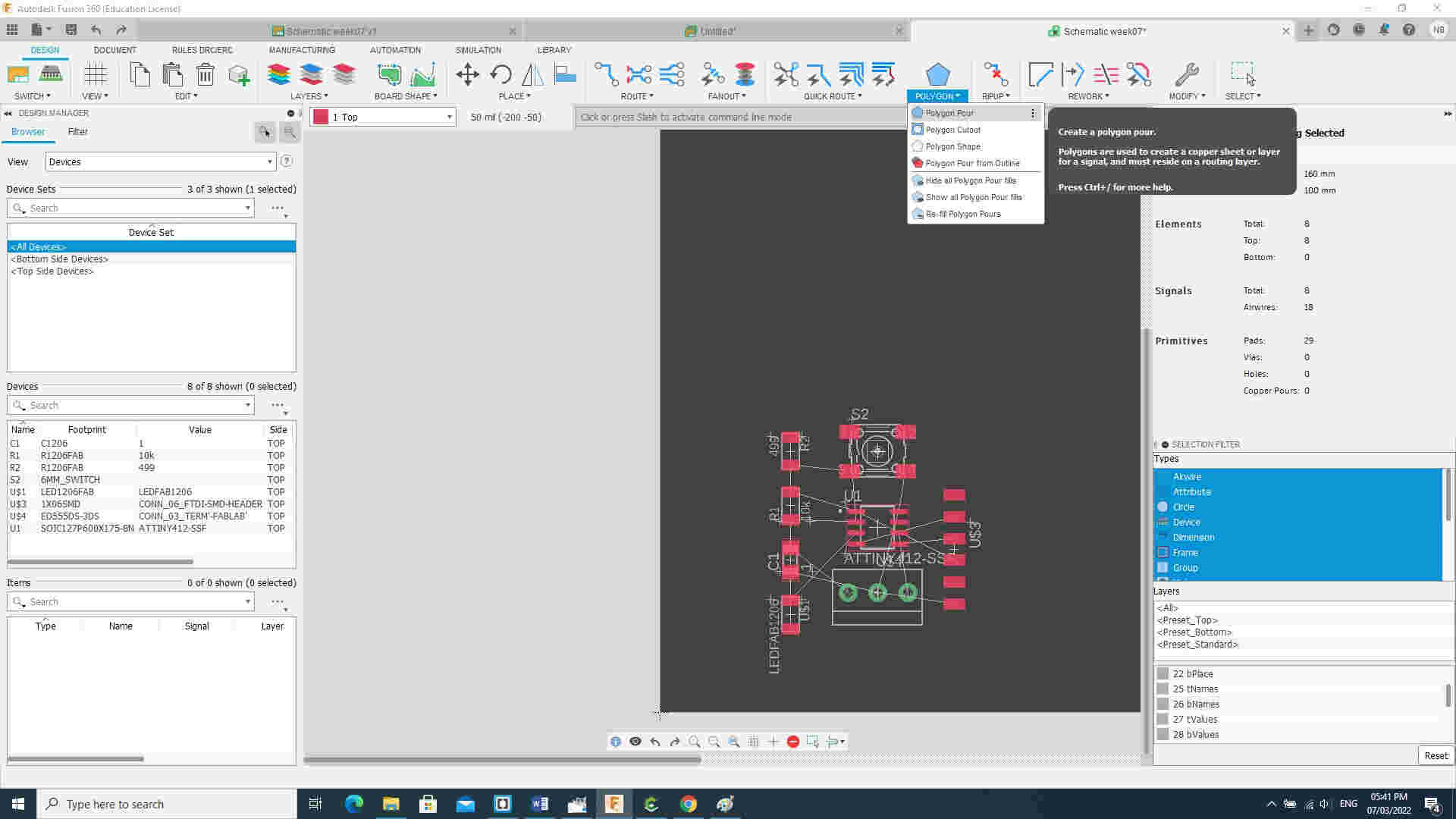
I moved and rotated the components to appropriate position using move and rotate tools. With Group tool one can move or rotate multiple components together.

Next I connected the components using net tool.

Schematic:
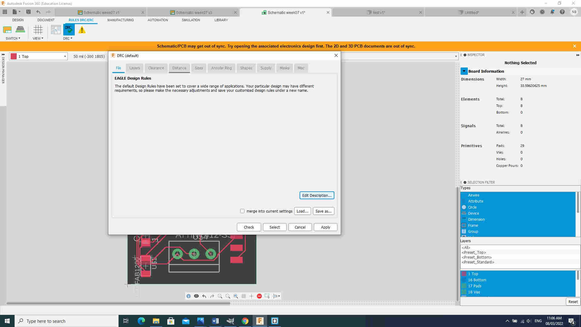
Design Rules Check

I downloaded the design rules files
I then used the SCR to BRD button to create the actual PCB
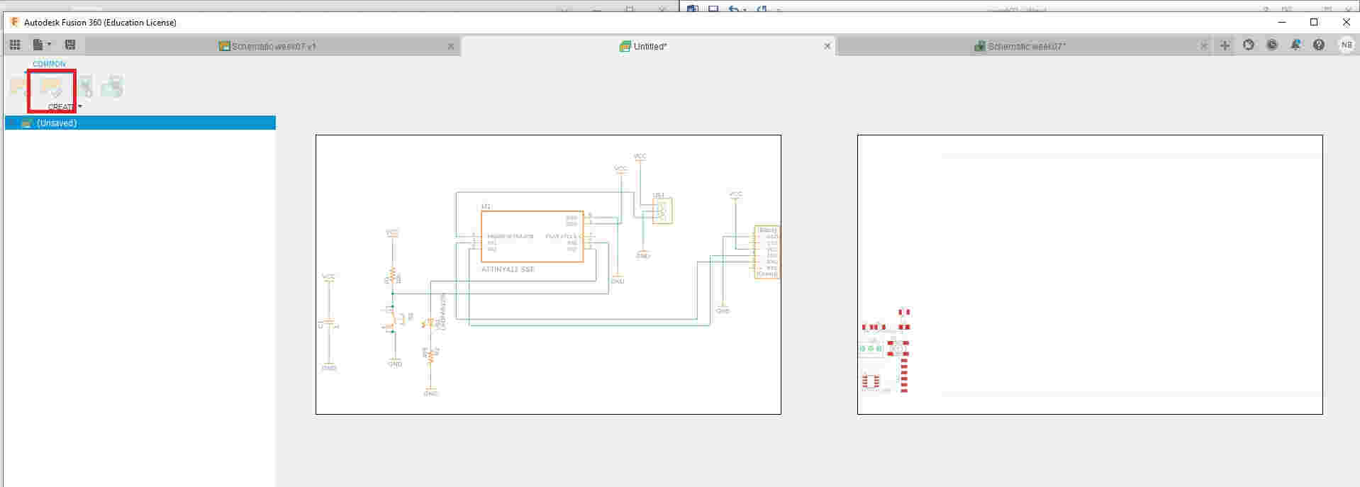
I then selected the “MOVE” tool to move the components and/or group of components


Create Pour Polygon
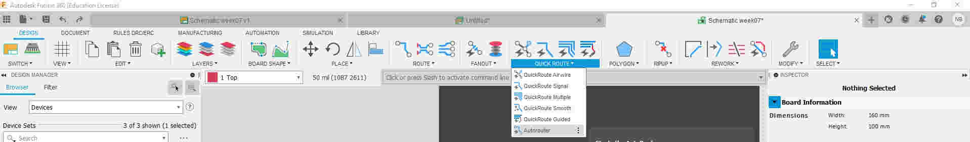
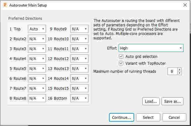
I the used the Autoroute for the traces
Change 16 bottom>N/A and effort > high >continue

After designing our board we need to check that the endmill we are using (#501 usually) is able to go between all the traces so the machine is able to cut successfully the board. For that we are going to use Design Rules Check (script) that will check that there is enough space everywhere.

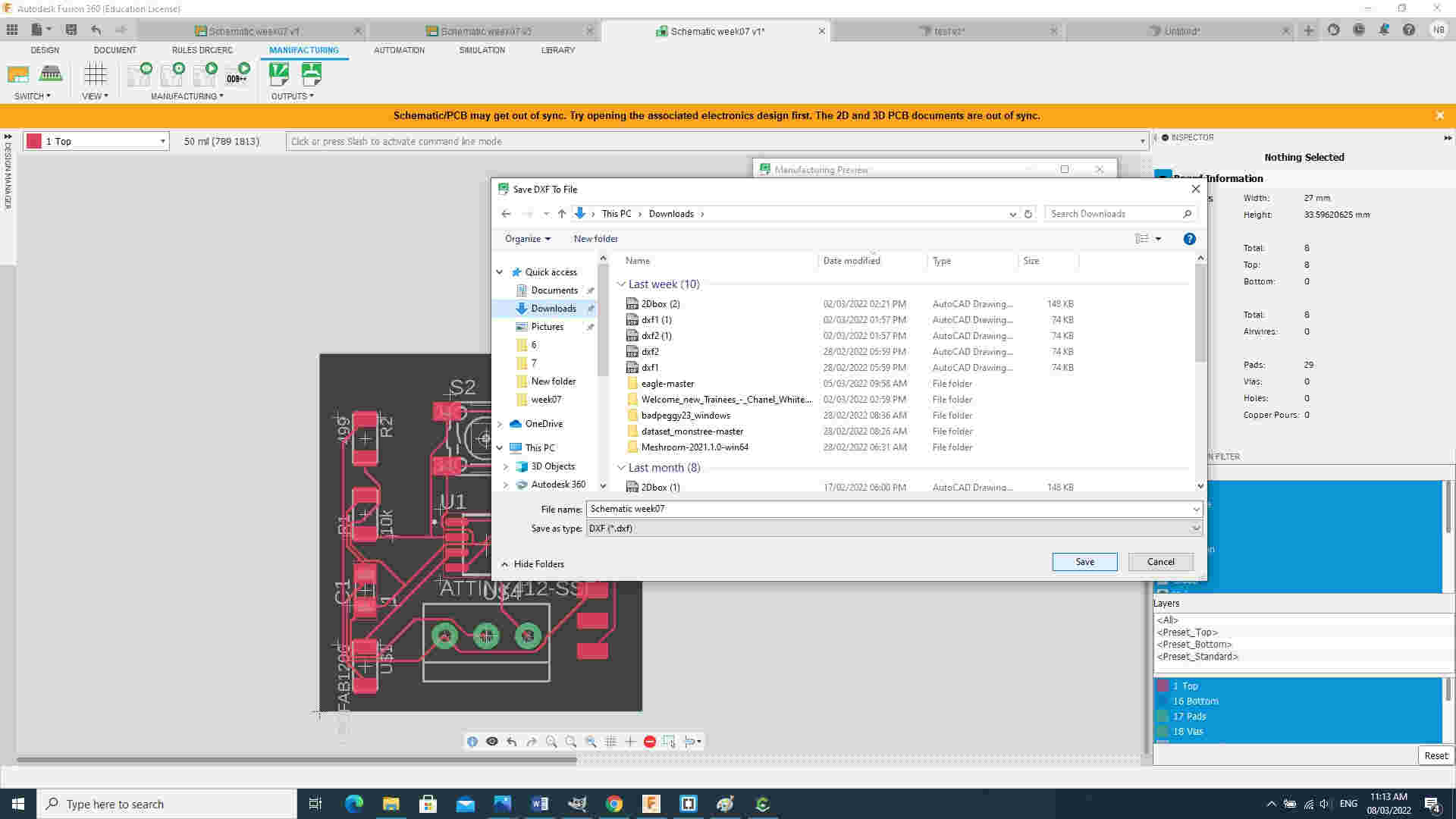
Exporting a board design
I on the Manufactouring tab in Fusion> preview
i then selected export to dxf and saved file.

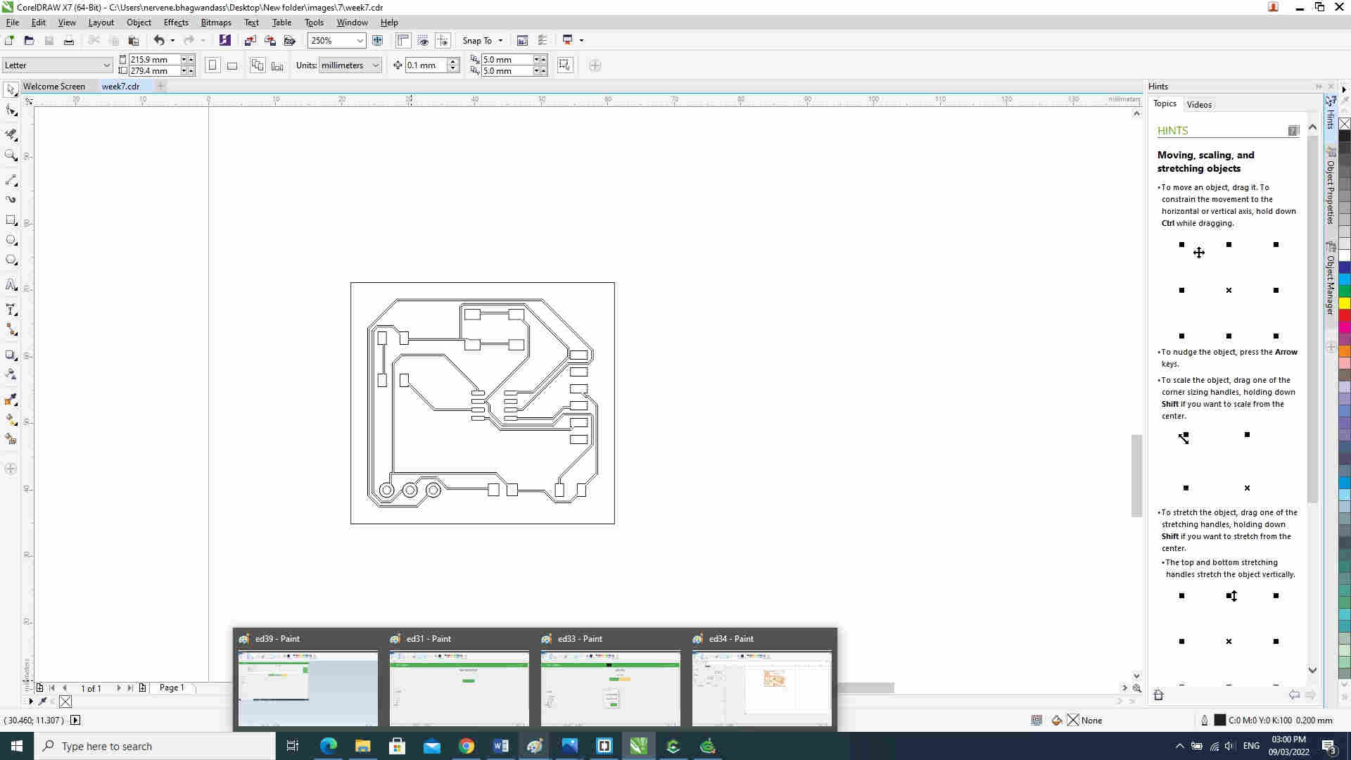
PCB process
Import the Schematic week07.dxf file in Corel Draw . I made some additions edits to the board and exported to .svg file
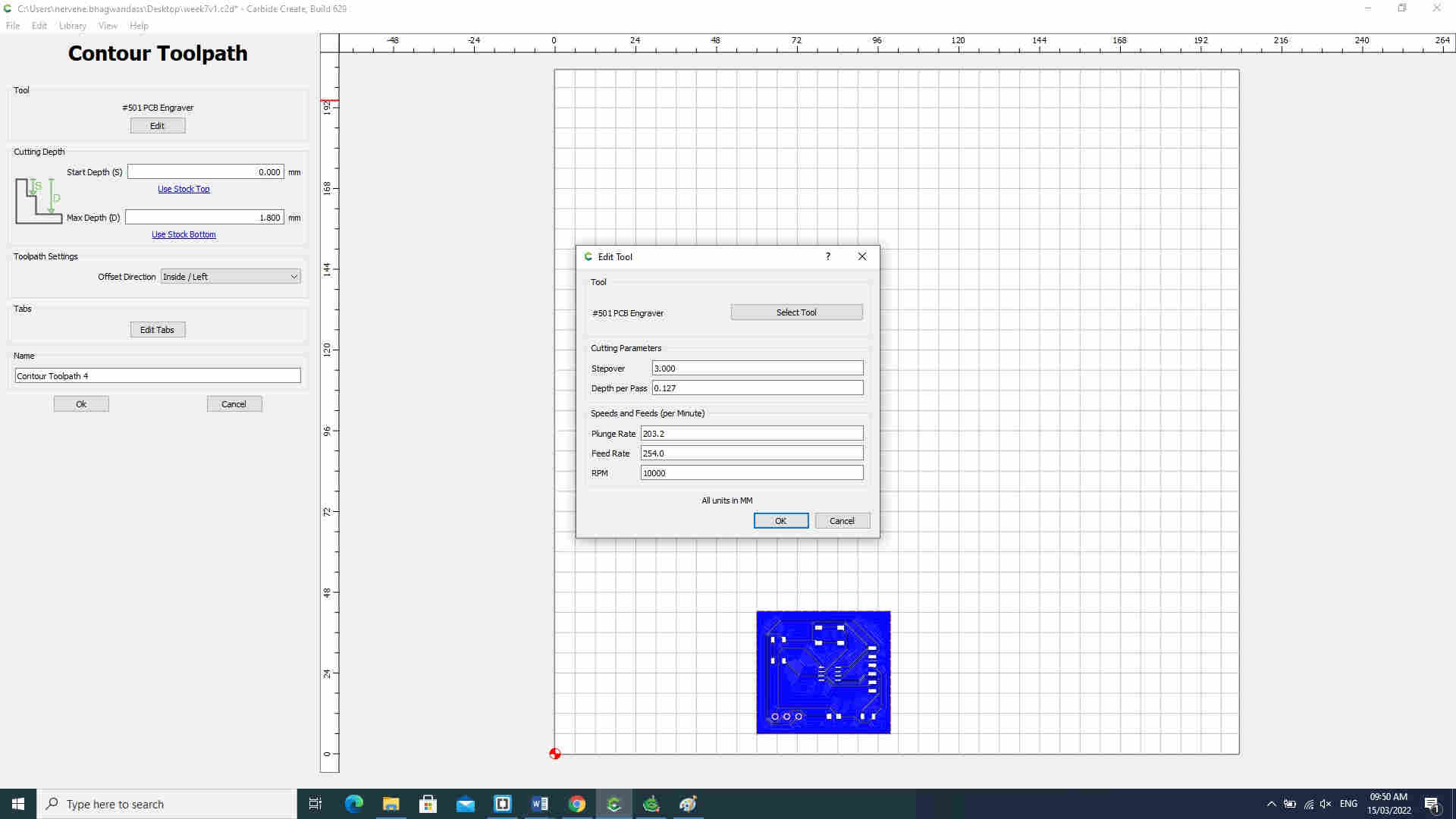
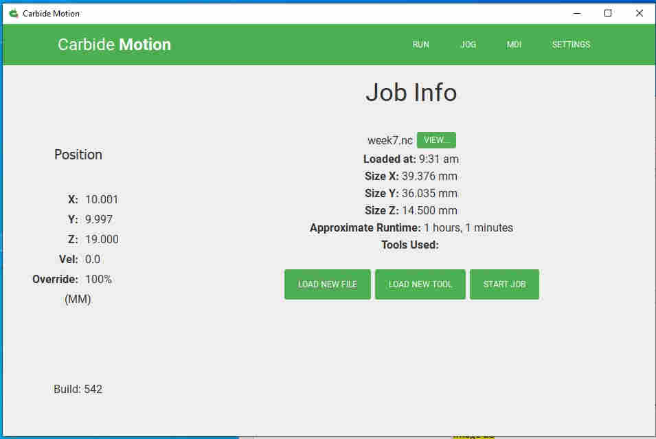
Import file in Carbide Create , place/postion job ,setup the toolpaths and save g code

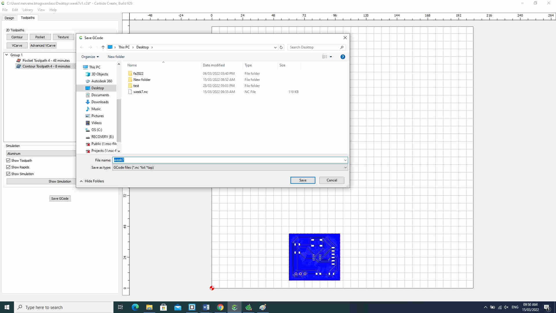
I connected to mill and went through the jog process in Caribede motion as previously documented in assignment 5 and then load week7.nc file
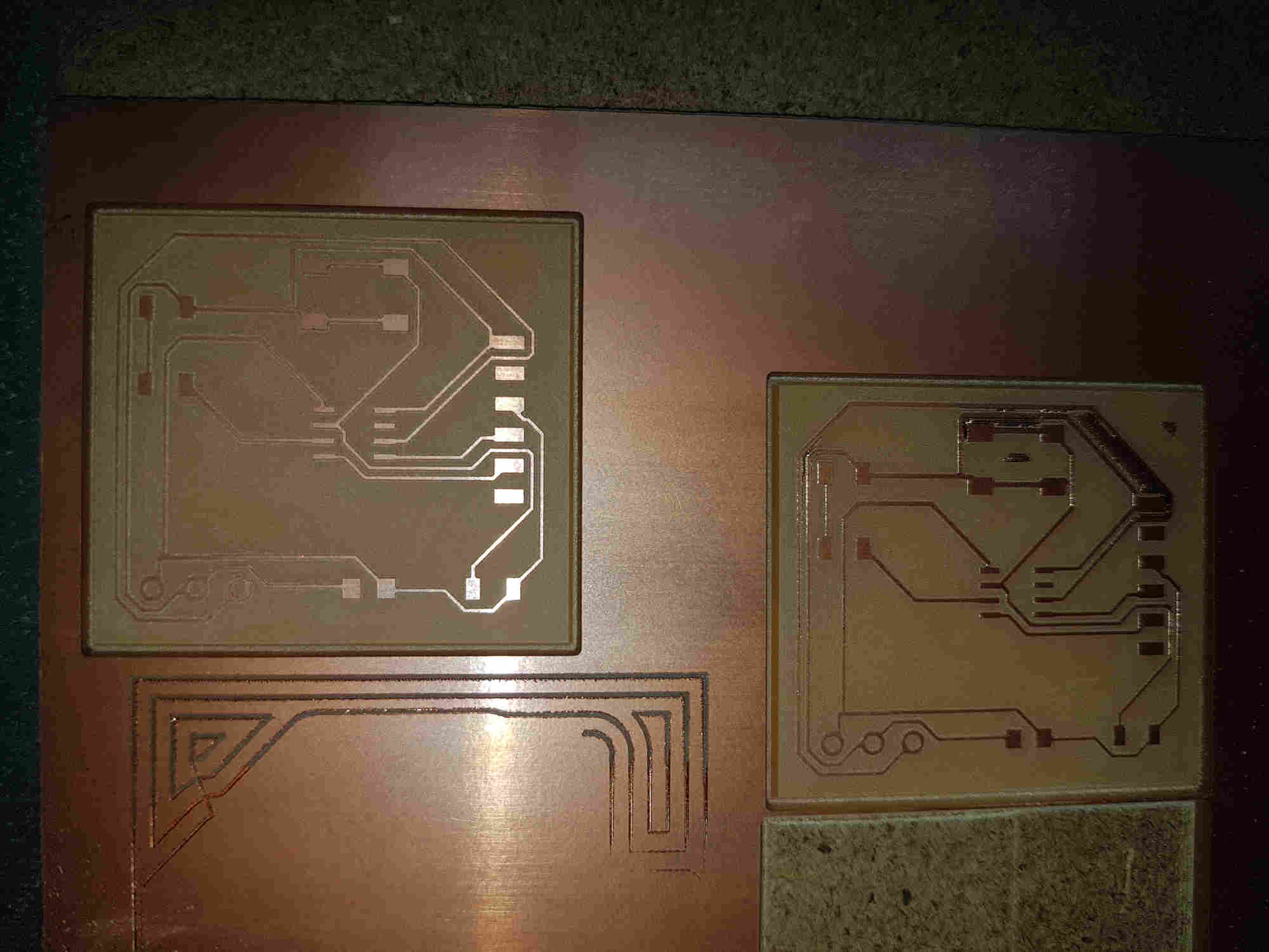
Milling and assembly!
I had some challenges dialling the pocket depth due the bit type and tracing width.
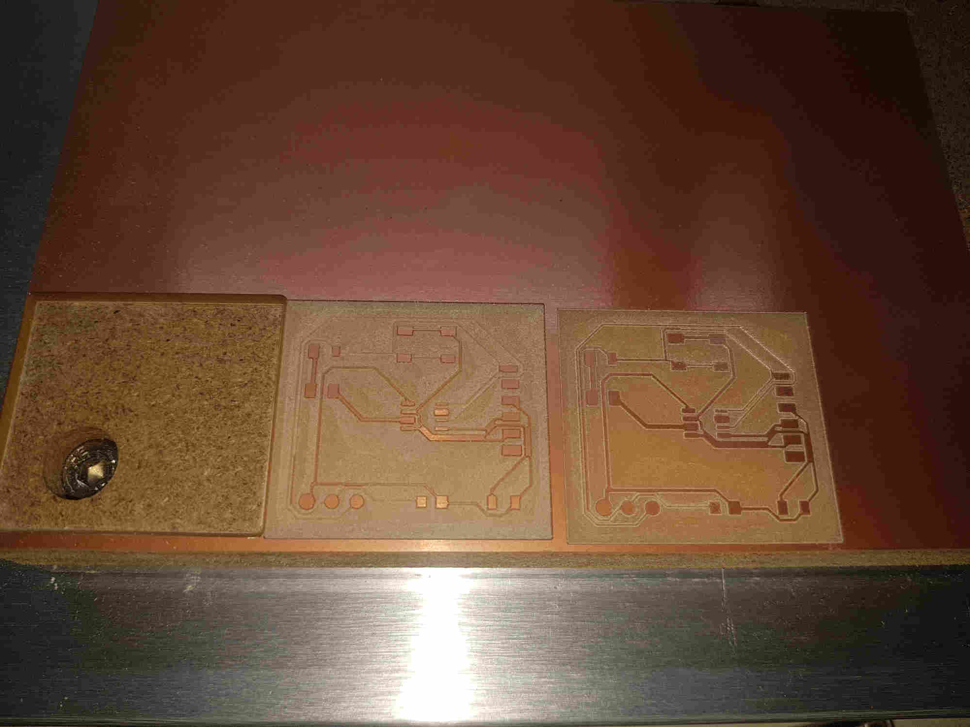
I corrected this by adjusting the tracing width ( making it wider) and pocket depth (decreasing the depth) I did get some success but it also highlight there can be defects in the copper board.
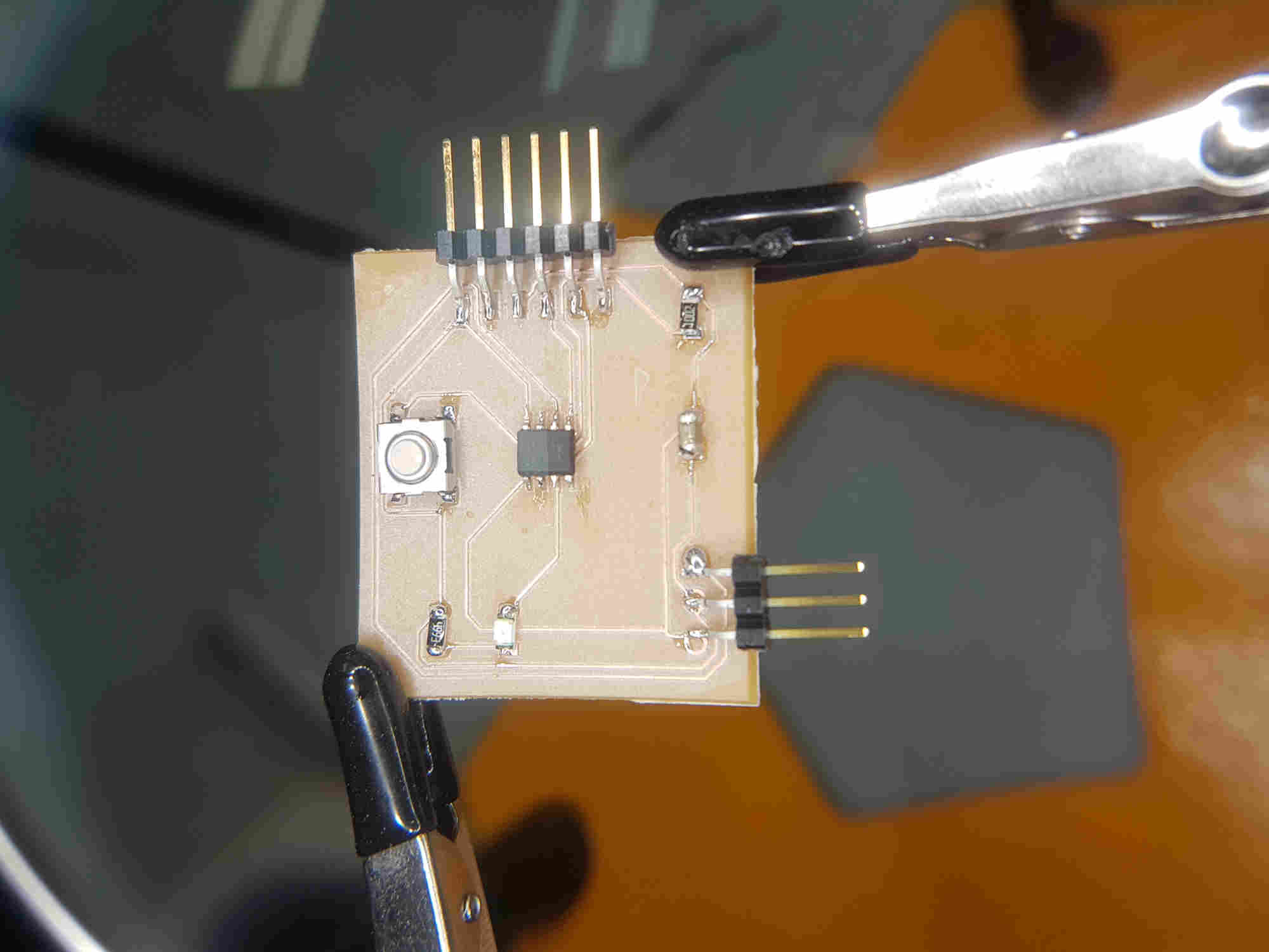
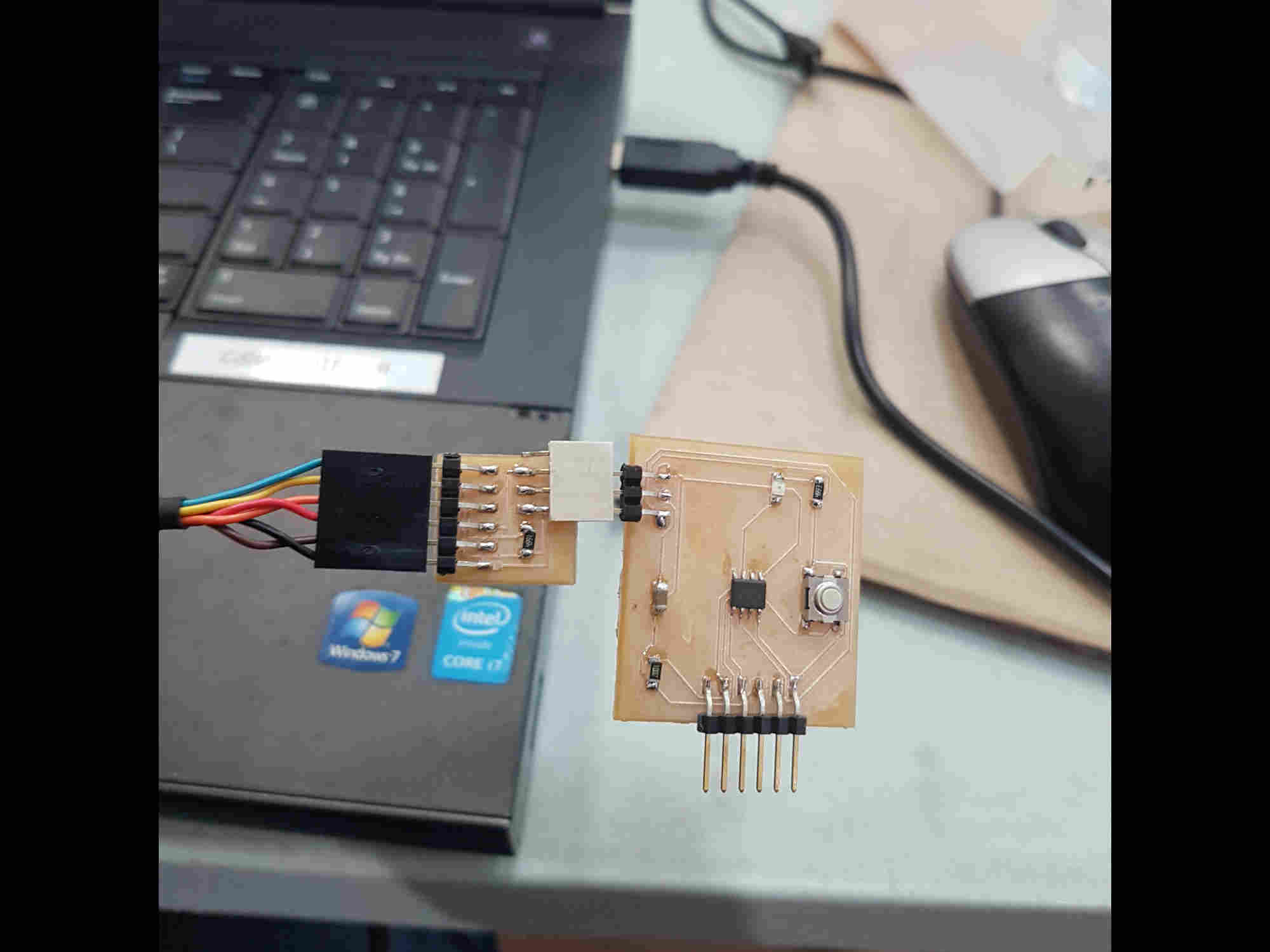
Soldering Circuit
I first located all the components for required for the PCB.

I then began soldering the IC Attiny 412 SSF to the board.
Note: Alway ground yourself while handling the IC
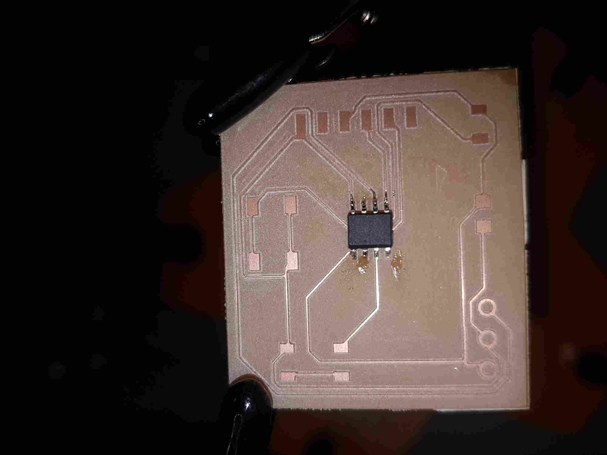
The other components followed.
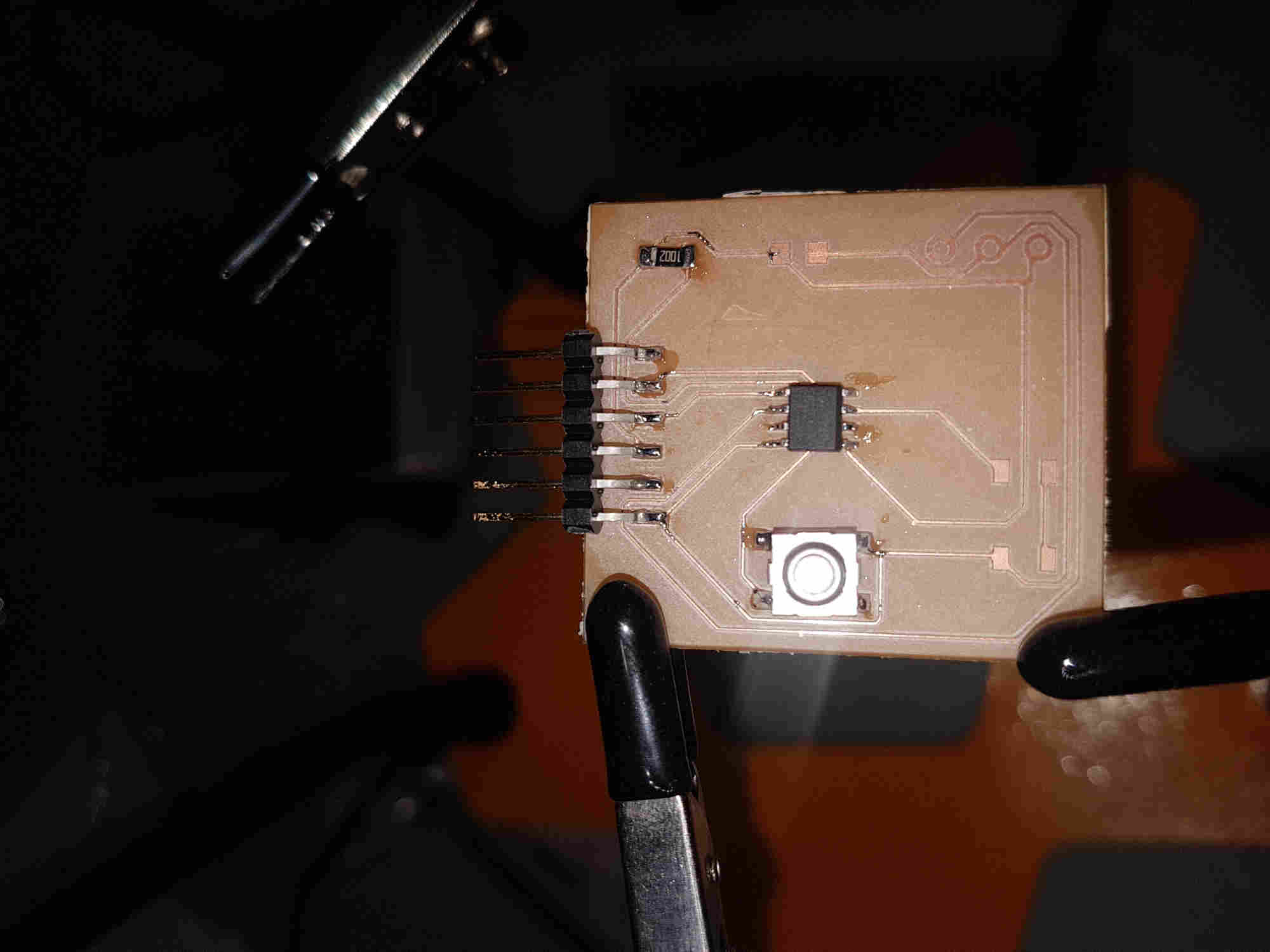
I completed soldering all componets

Programming
I first download and installed the Arduino software.
I open the from Fab academy and copy it. http://academy.cba.mit.edu/classes/embedded_programming/t412/hello.t412.echo.ino
I then open the Arduino software and paste the code.

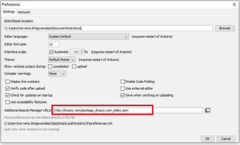
I then set up the preference, and copy the URL (http://drazzy.com/package_drazzy.com_index.json) here.
Then I set the board manger Tool>Board manger>search Attiny and megaAVR and install.
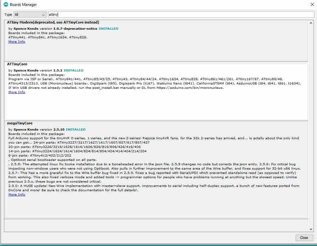
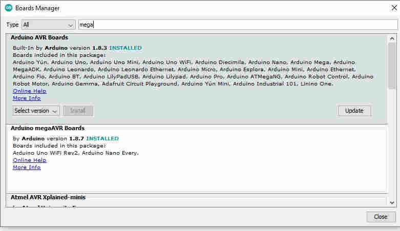
Then in tool-board select the ATtiny412/402/212/202 and in chip select -ATtiny412, Port-(my board).

Then I verify and uploaded the code.

Success !

Useful links
- Autodest
- Youtube
- Microchip ATTINY 412
- Fluke -Circuit specialists -electronics-notes
- youtube
- Fluke
- testequipmentdepot
- bkprecision