5. Electronics production
Electronic production is a term use for designing, assembling, producing, and testing electronic components and printed circuit board (PCB) assemblies for original equipment manufacturers.
Learning outcomes
-
Described the process of milling, stuffing, de-bugging and programming
-
Demonstrate correct workflows and identify areas for improvement if required
Like the previous, student are expected to complete two (2) categories of weekly assignment.
-
Group assignment:
-
Characterize the design rules for your in-house PCB production process: document feeds, speeds, plunge rate, depth of cut (traces and outline) and tooling.
-
document your work (in a group or individually)
-
Document your work to the group work page and reflect on your individual page what you learned
-
-
Individual assignment:
- Make an in-circuit programmer that includes a microcontroller by milling and stuffing the PCB, test it to verify that it works.
Milling Machine
Milling machines are a type of machinery used for the removal of material from a workpiece using rotary tool cutters. These type machines can drill, bore, and cut an array of different types of materials. This process of removing pieces of the material in line with the tool axis is known as milling, and thus the machines used in the process are called milling machines. Milling machines come in many types and are used across a variety of industries for this week lesson we would be using a desktop milling machine.
At the NIHERST Fablab we had access to:
- Model: Nomad 3
- Software: Carbide Creator and Carbide motion
-
Specifications:
- Cutting area: 8”(X), 8”(Y), 3”(Z)
- Outer dimensions: 17.5”(W), 19”(D), 17”(H)
- Spindle collet: ER-11, 7mm max cutter diameter
- Spindle RPM: 9000 - 24000 RPM
- Input voltage: 110V or 220V
-
Material:
Group Assignment
The Group Assignment page is as follows Link
Group Members:
- Nervene Bhagwandass
- Christopher Proute
- Terrence Carew
- James Khan
- Marvin Holloway
- Ravi Baldeo
Individual assignment
PCB process
Downloading the serial UPDI + VCC Traces - Serial UPDI + VCC Traces

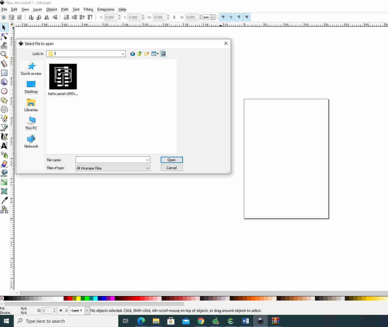
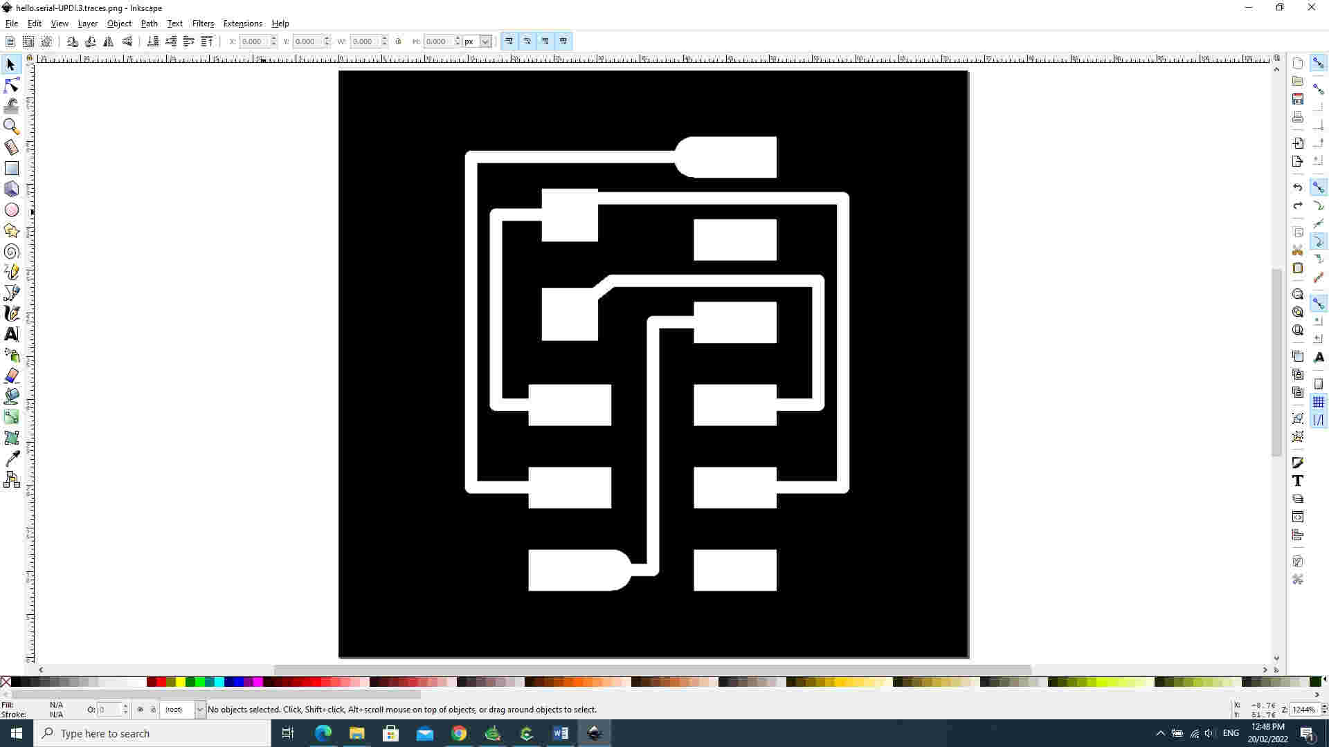
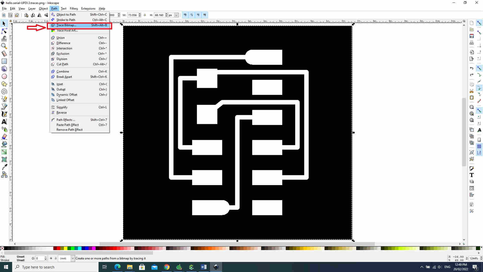
- Open the hello.serial-UPDI3.traces.png file in Inkscape
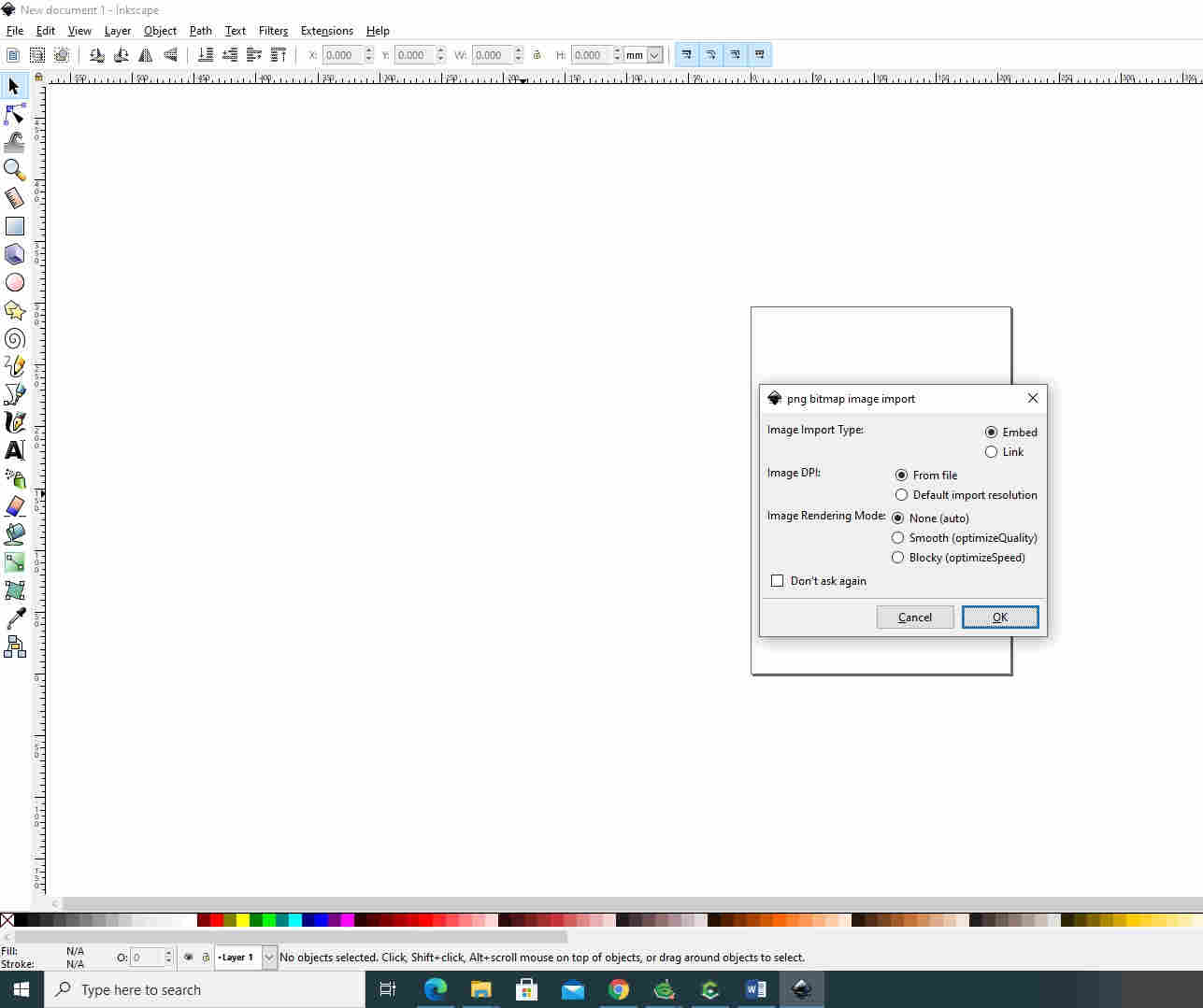
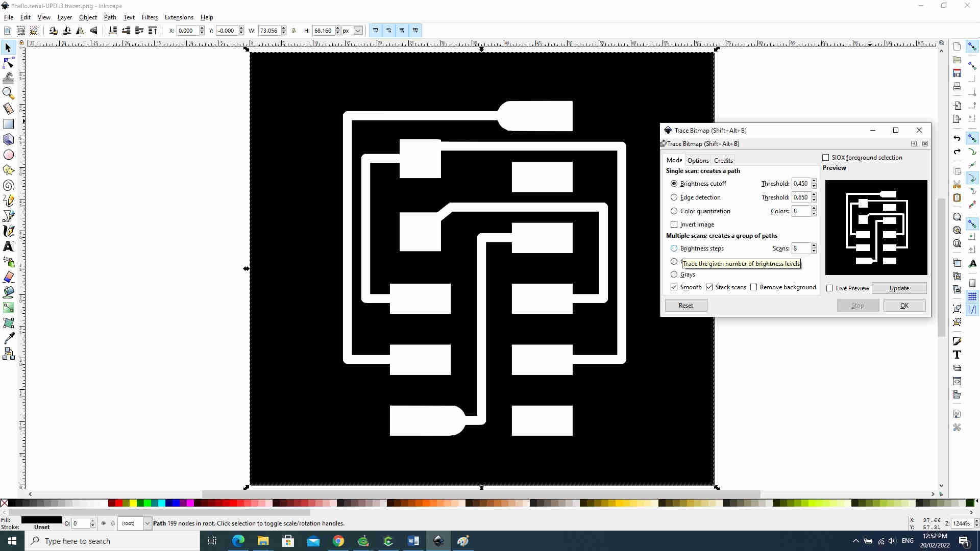
- Would now need to Trace bitmap of the image : Path> Trace bitmap
- The default setting should be fine, click OK
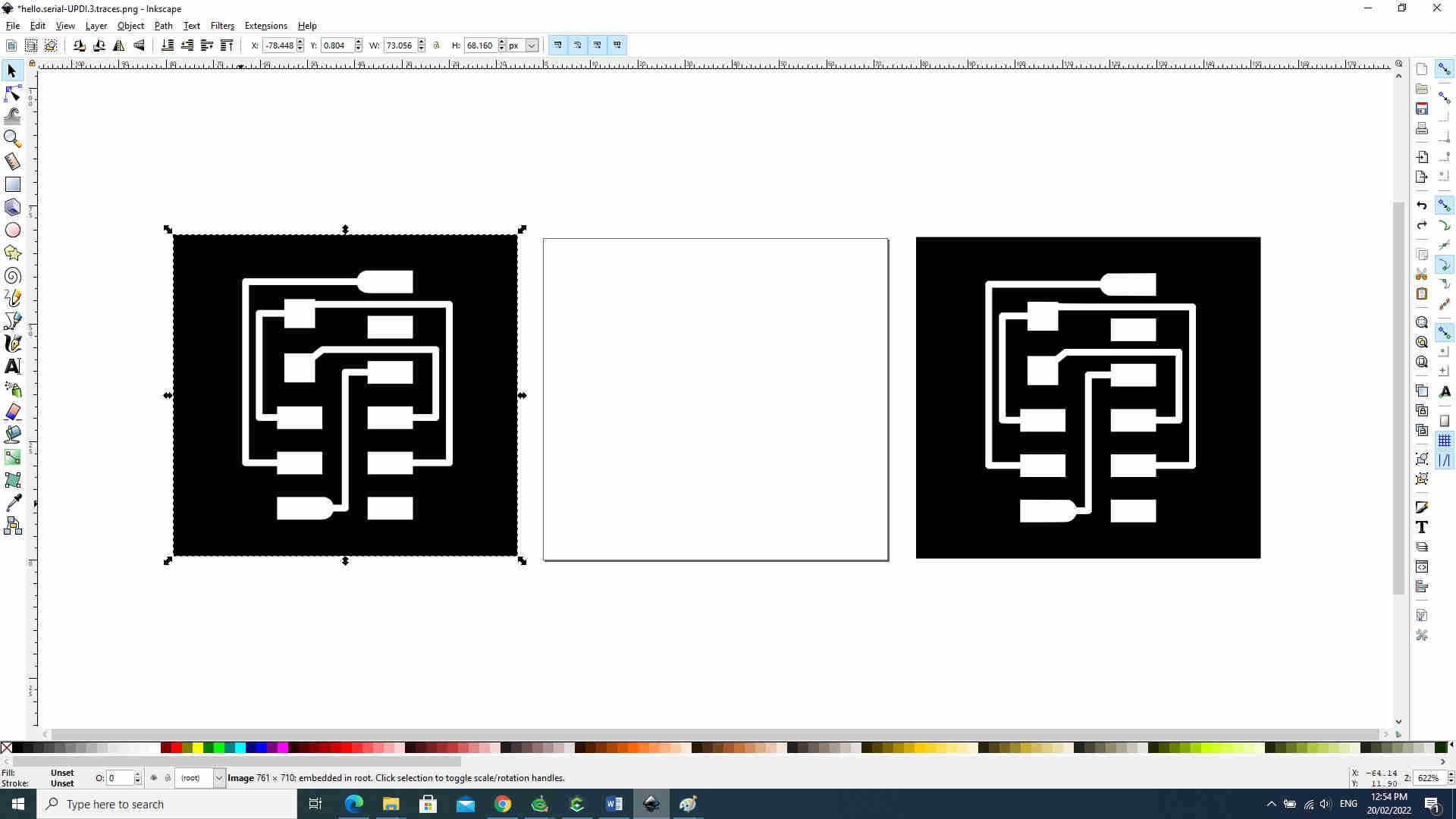
- Would then need to separate the traced shape from the original and delete the original
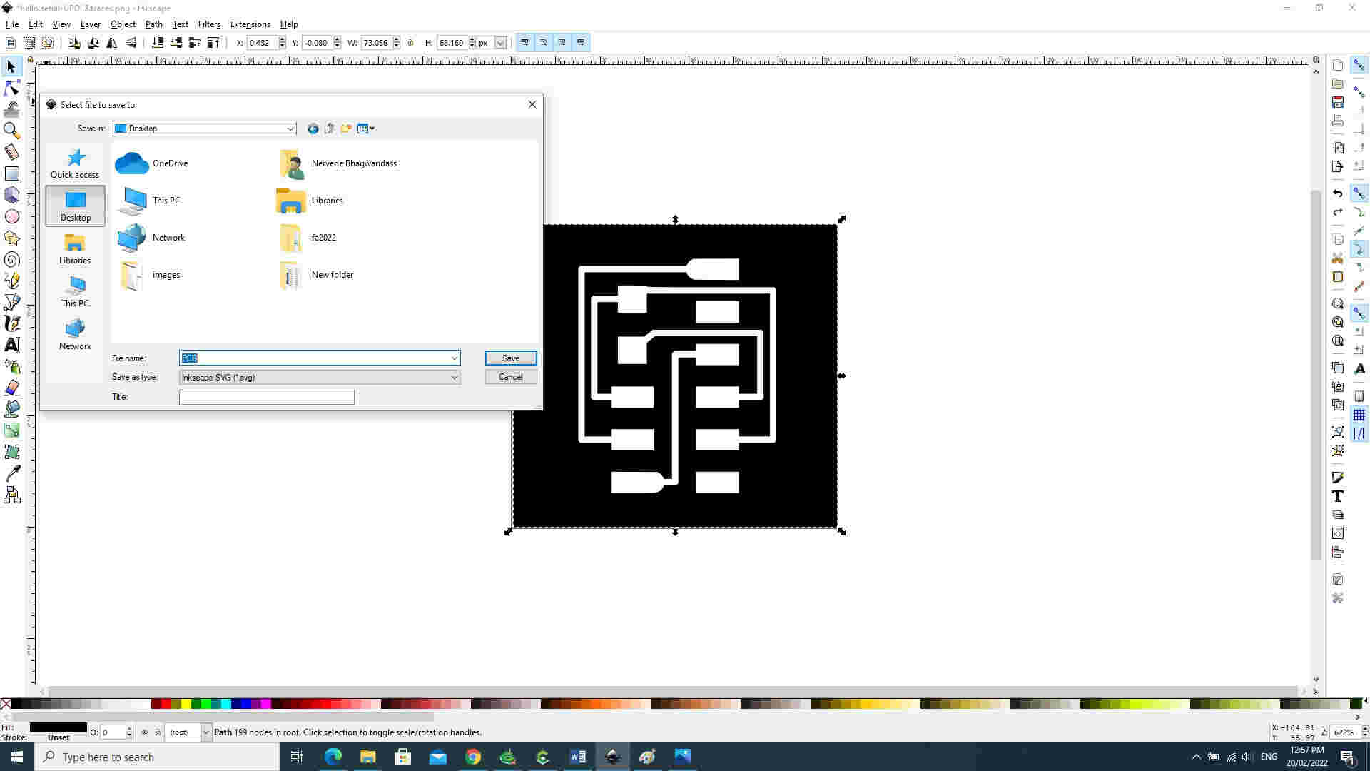
- Now save the file as a .svg file “PCB”
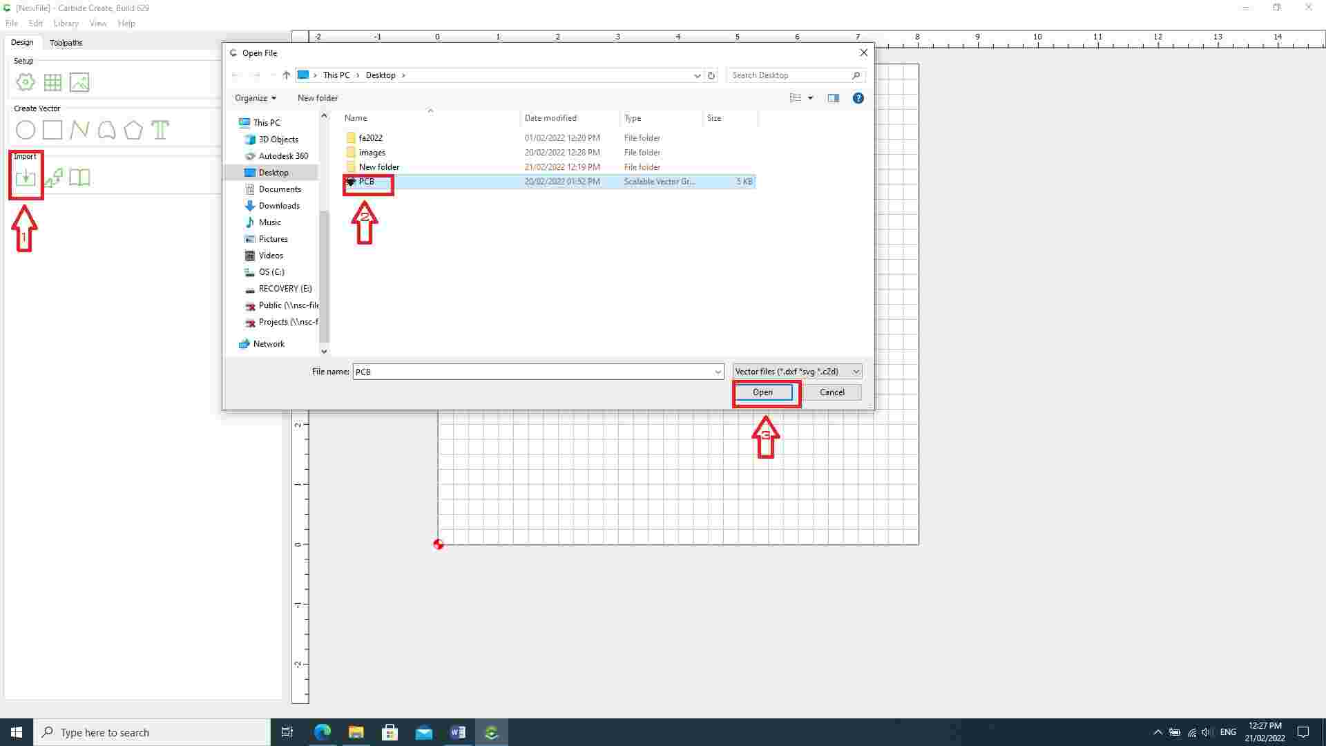
Setting up Carbide Create
Open Carbide Create ,set units to mm and import “PCB.svg” and click open

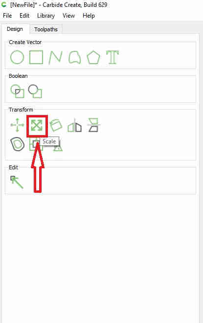
Scaling the PCB
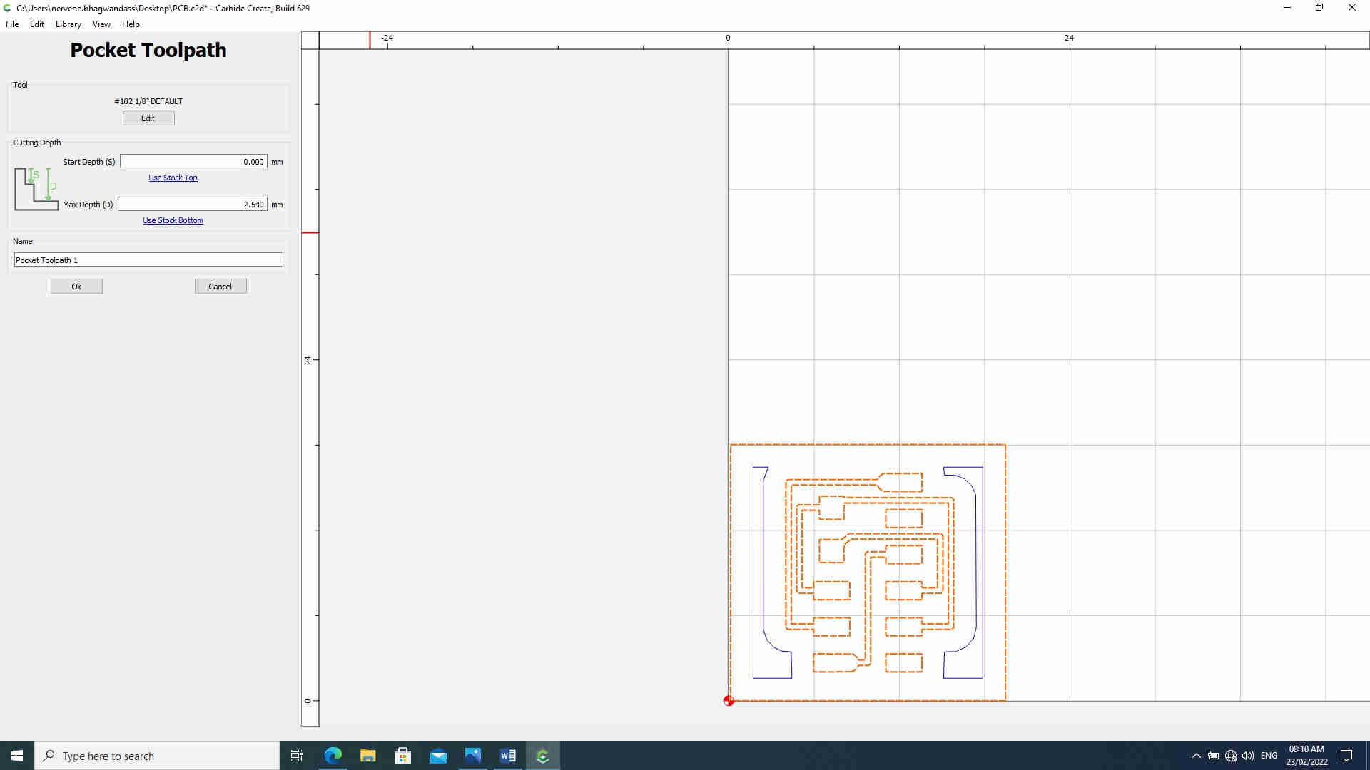
Toolpaths tab> Pocket

Select “Edit” under Pocket Toolpath
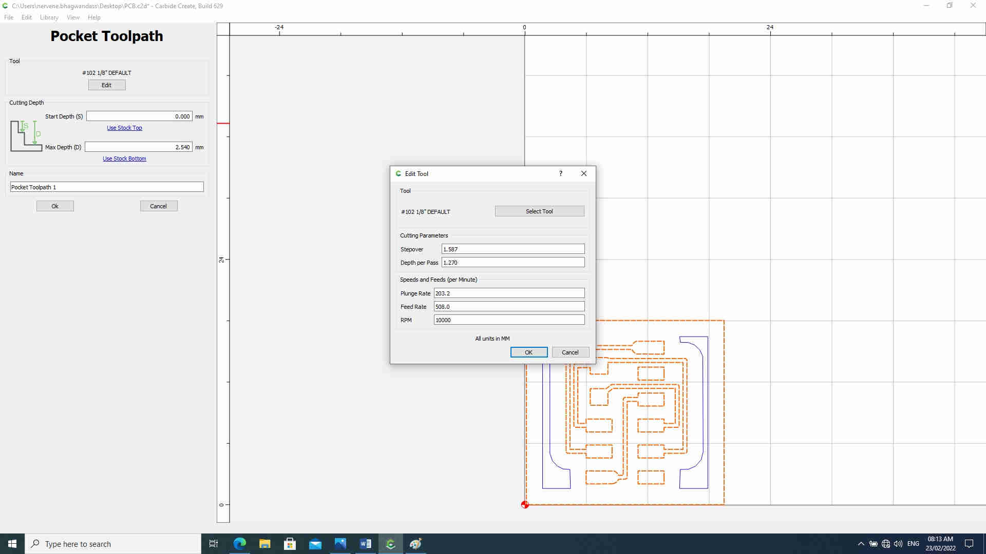
Click “Select Tool”

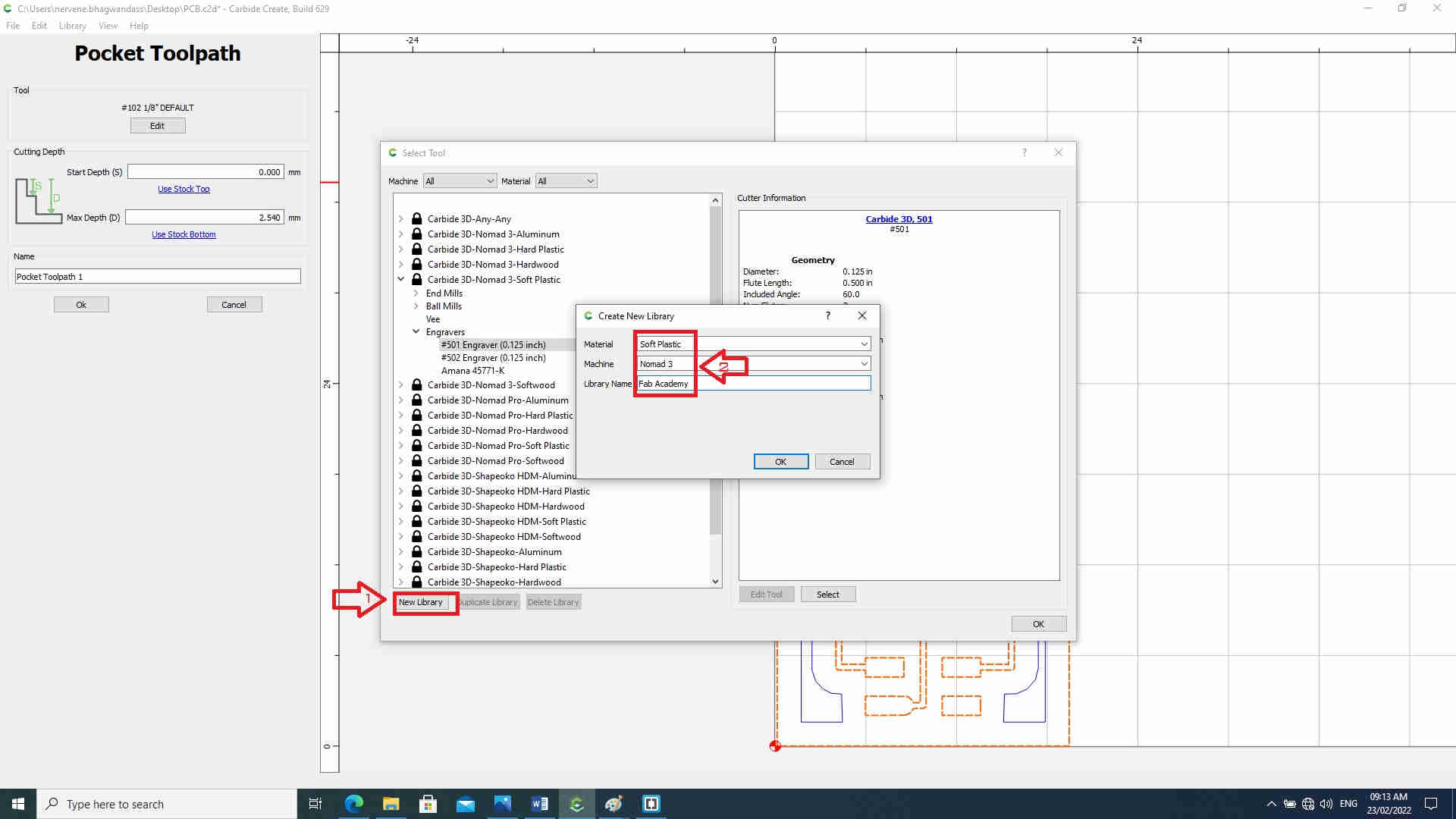
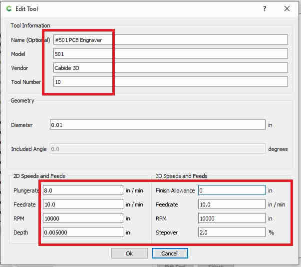
“Carbide 3D Nomad 3 Soft Plastic> Engraver> #501 Engraver (0.125inch)
Select “New Library” at the bottom left corner
-
Material: soft plastic
-
Machine: Nomad 3
-
User: Fab Academy
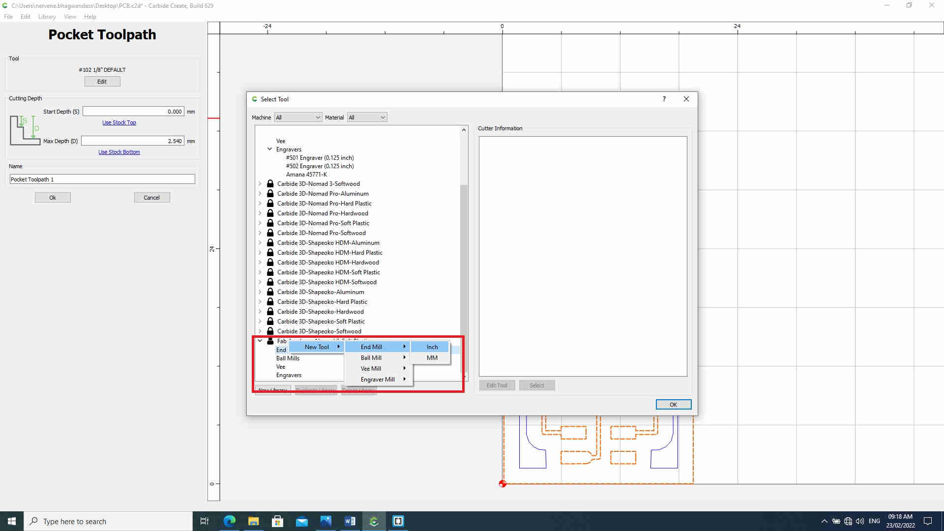
Right click on “End Mills” and select “Inch” under New Tool>End Mill>Inch

Follow the photo and change the fields accordingly
After creating the 501 toll profile, select that, and click ok.
Before clicking ok again, copy the number under “Depth per Pass”. Click OK. Pasta valve in “Max Depth”

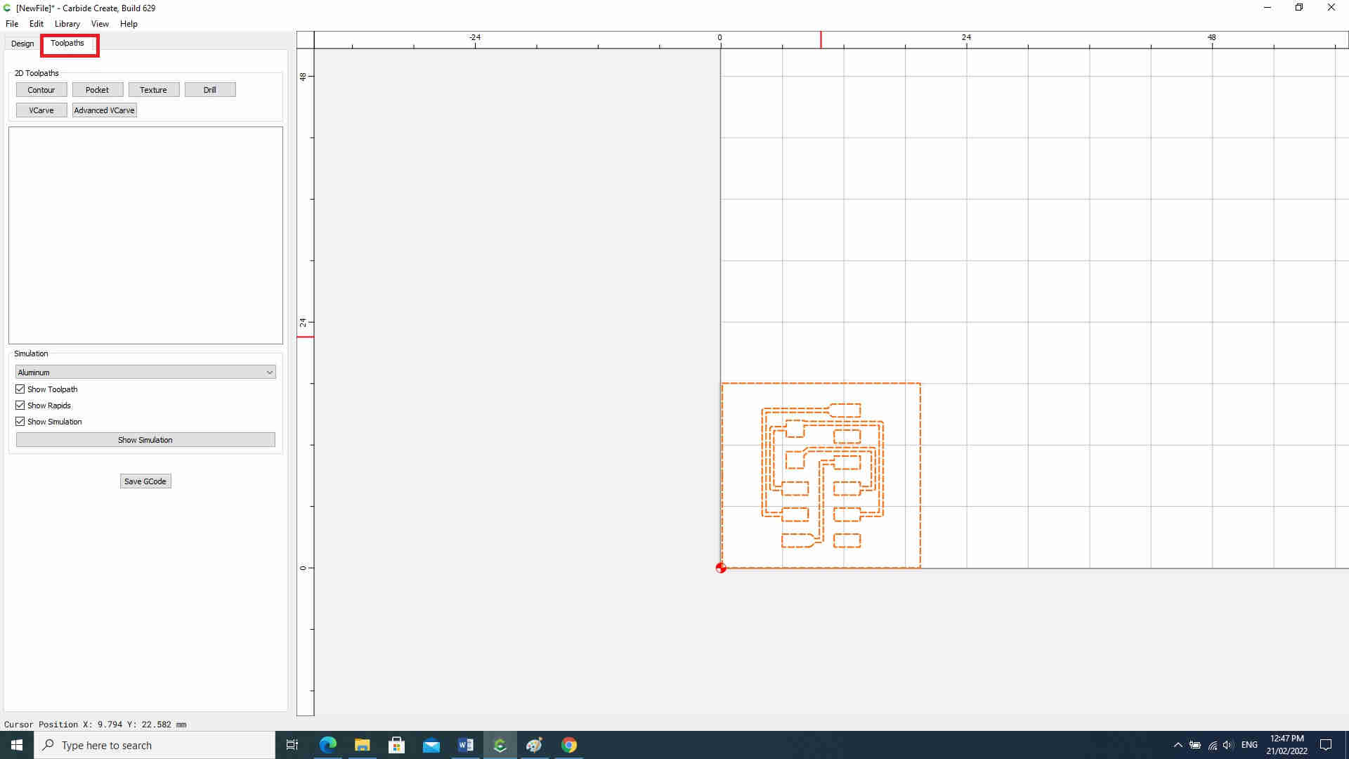
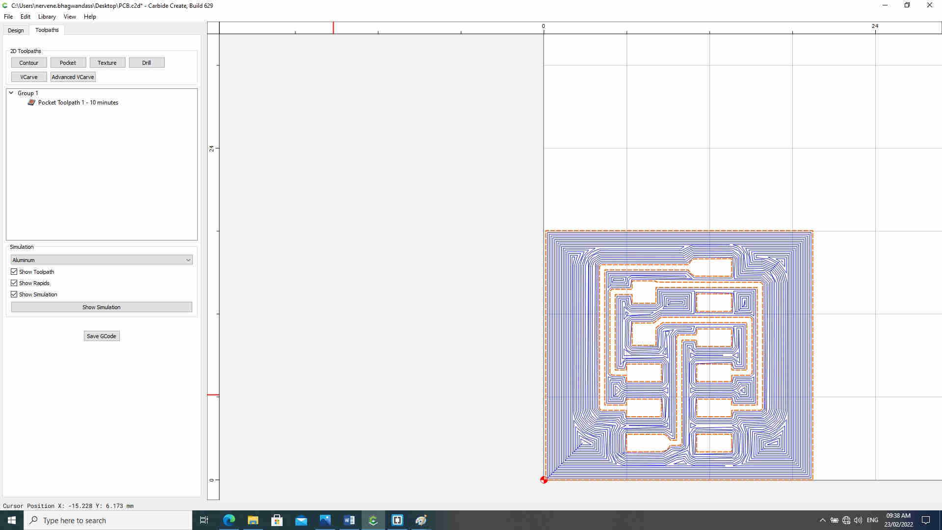
You should be able to see the tool path that will take out the unwanted copper.
Select only the outer path, and click “Contour”, we will create the cut out tool path now
Select #112 under Soft Plastic. (You are free to use a thicker or thinner end mill to achieve this, depending on your PCB’s shape.) Click OK
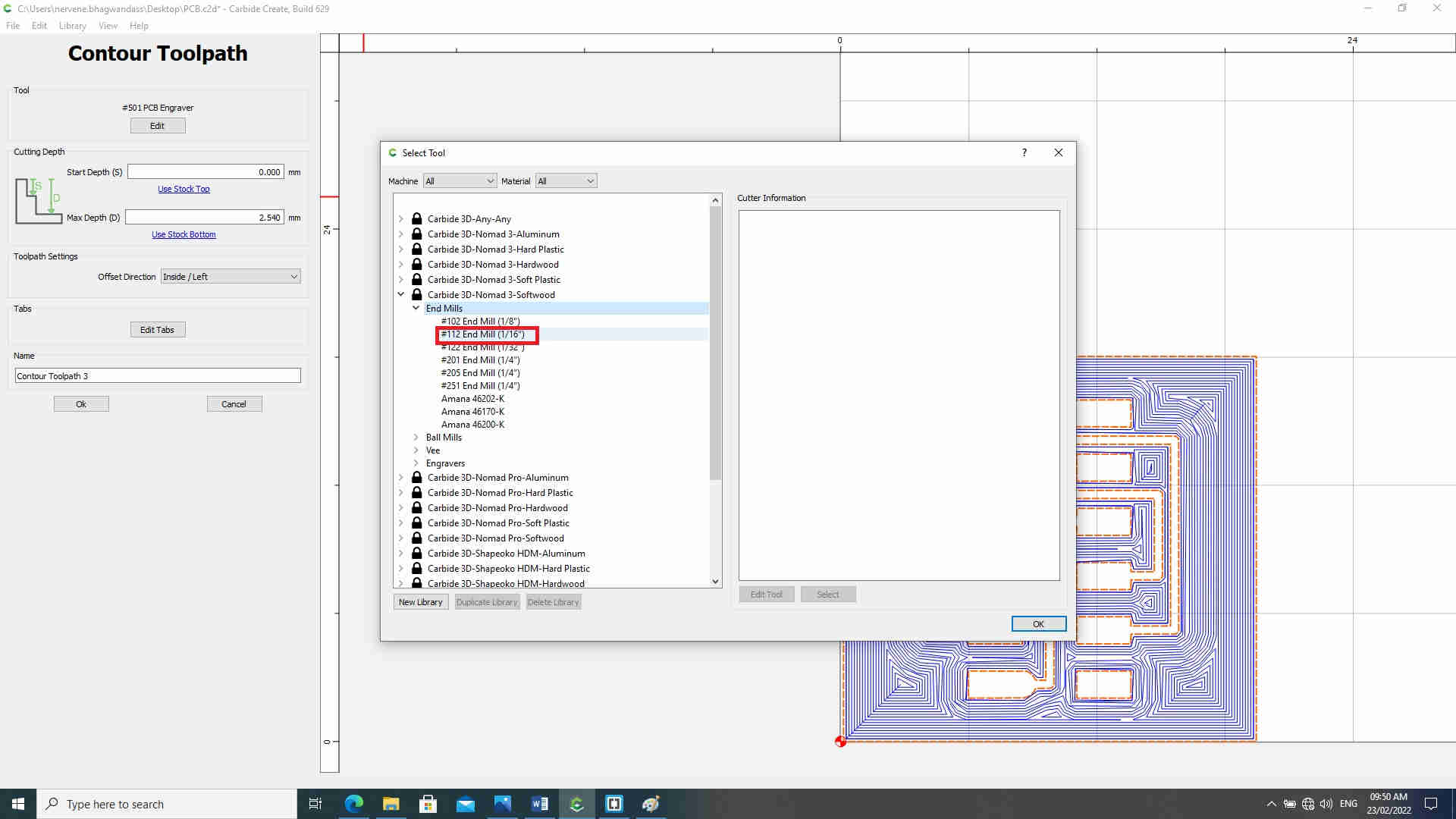
Double check the number and click OK again
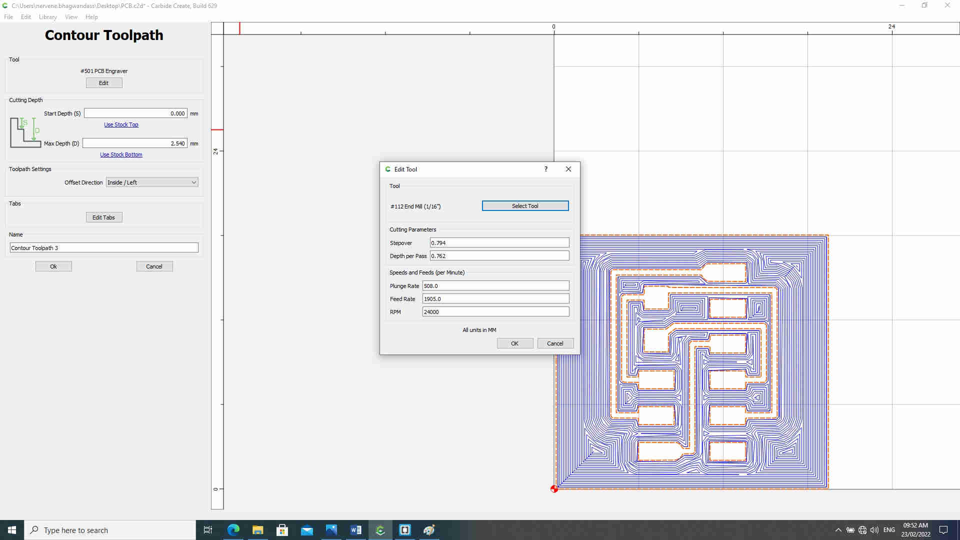
Input the PCB’s thickness in “Max Depth”. Click OK.
Now we have both tool paths for milling and cutting the PCB. Click “Save GCode”.
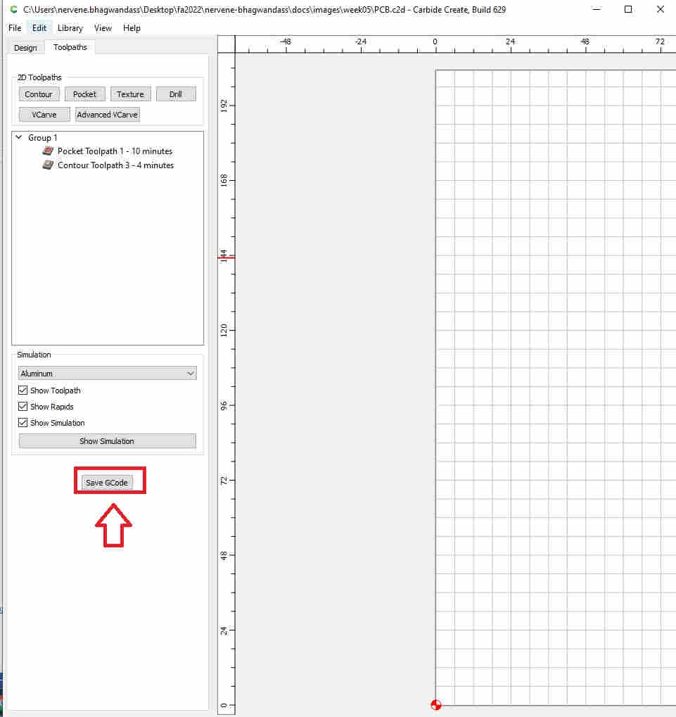
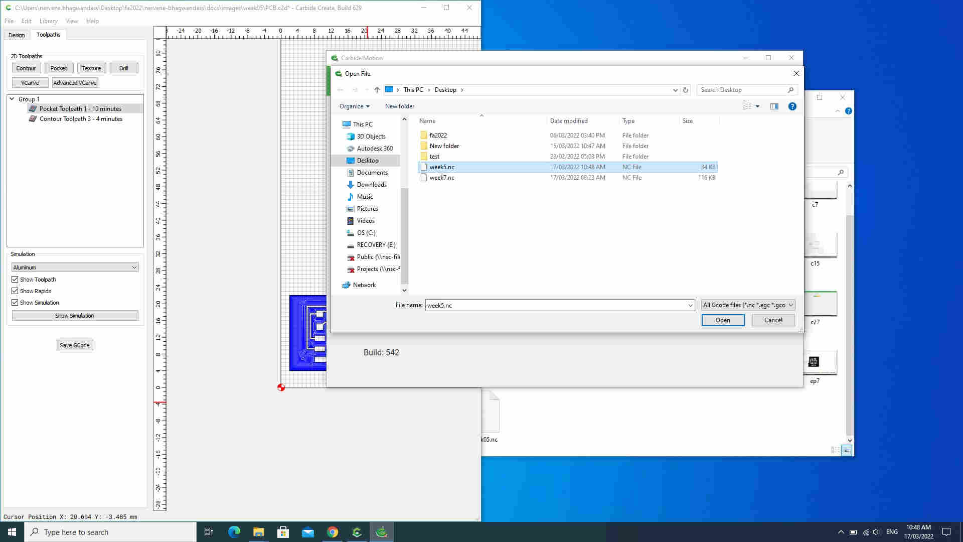
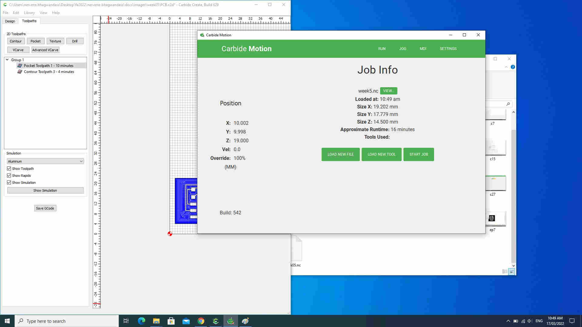
Save the GCode.

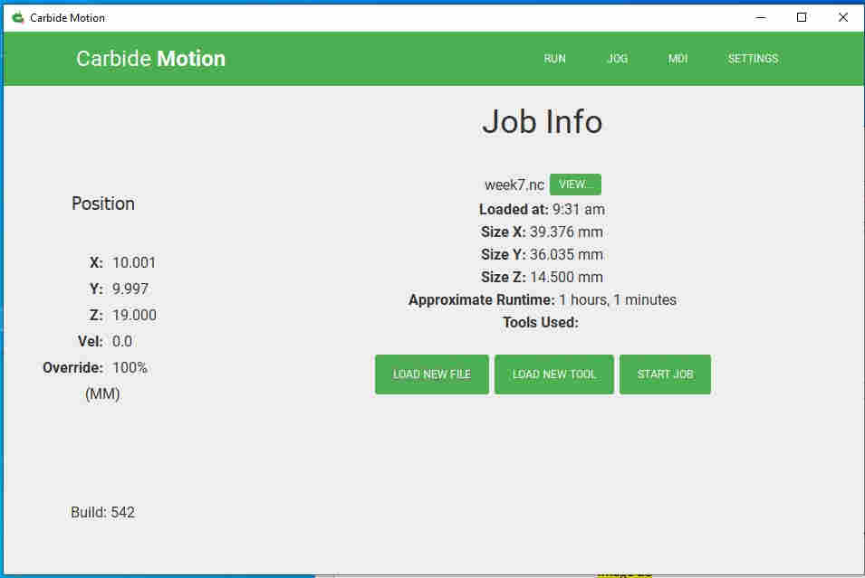
This is the GCode .nc file that we will open with Carbide Motion to mil the PCB
Setting up Carbide Motion
Open Carbide motion
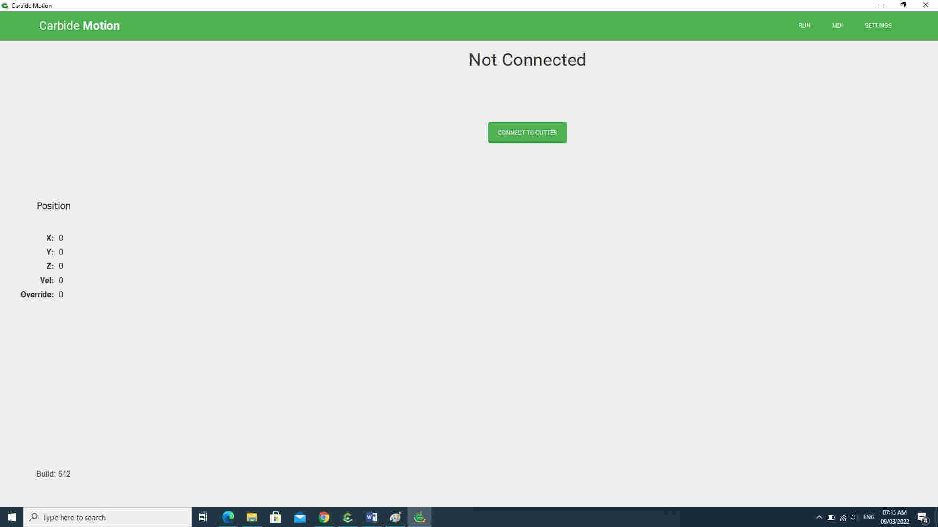
Connet to cutter
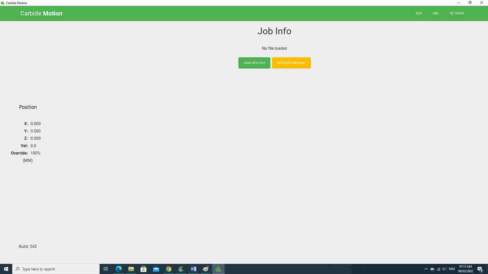
Intialize machine
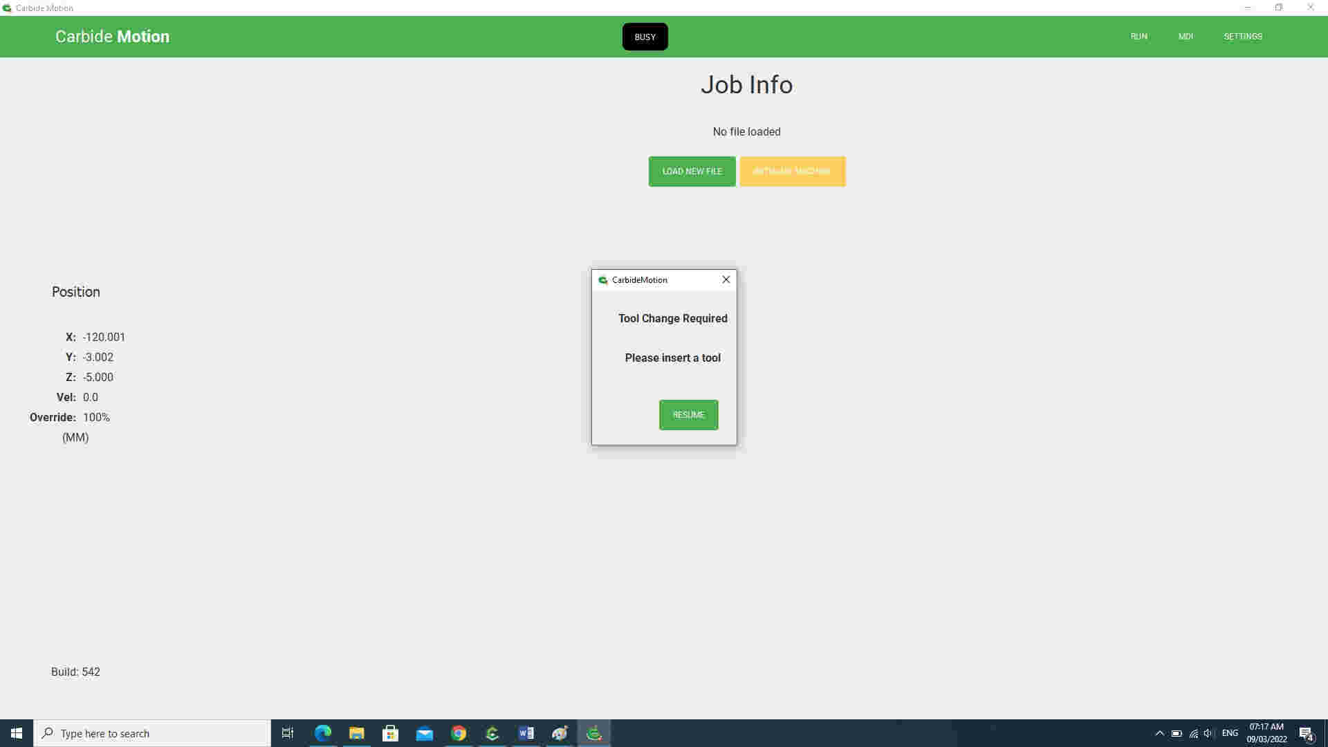
Insert tool
Then I Jog the machine as indicated in the group assignment section after which I load the g code

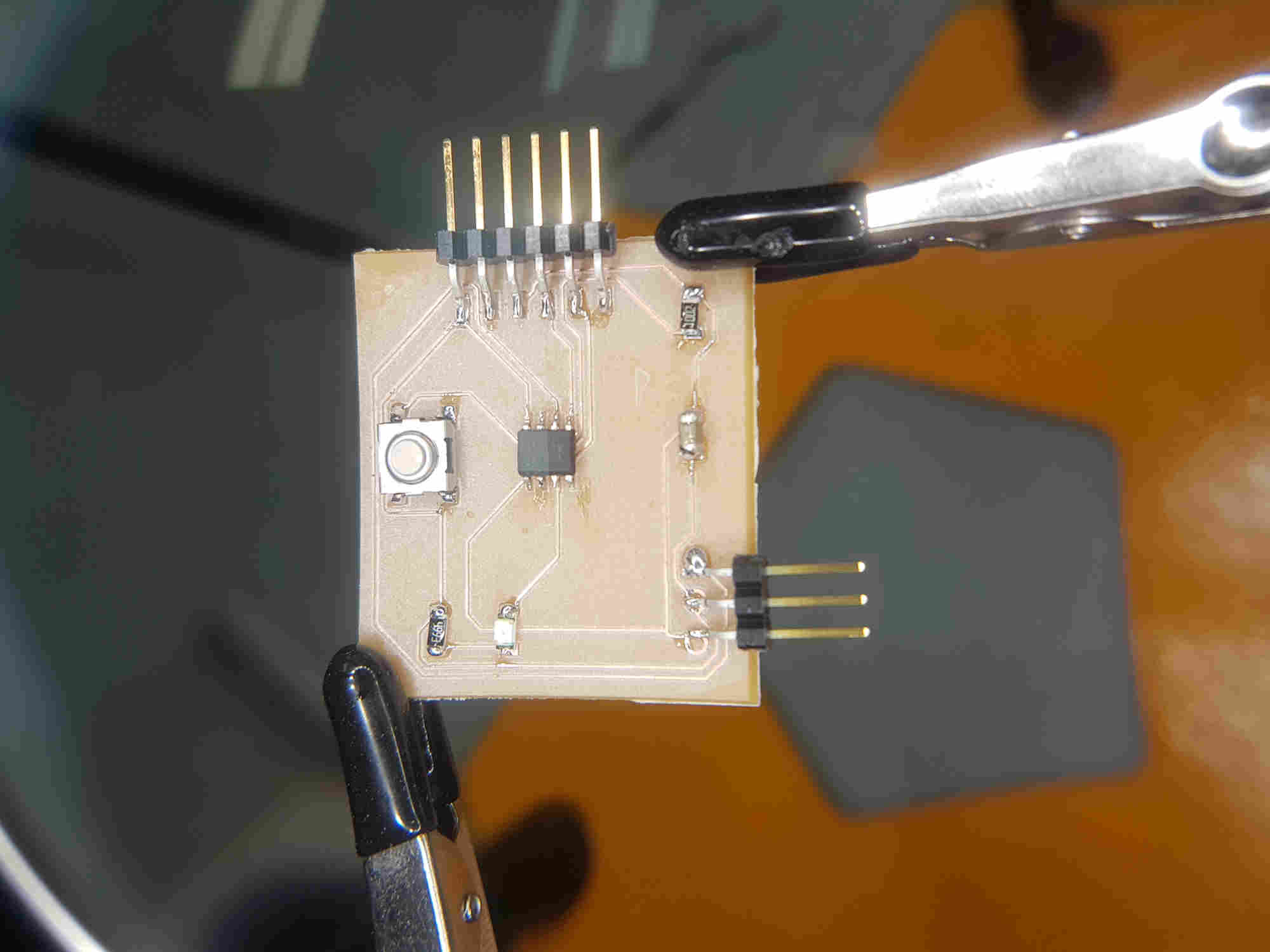
Milling and assembly!
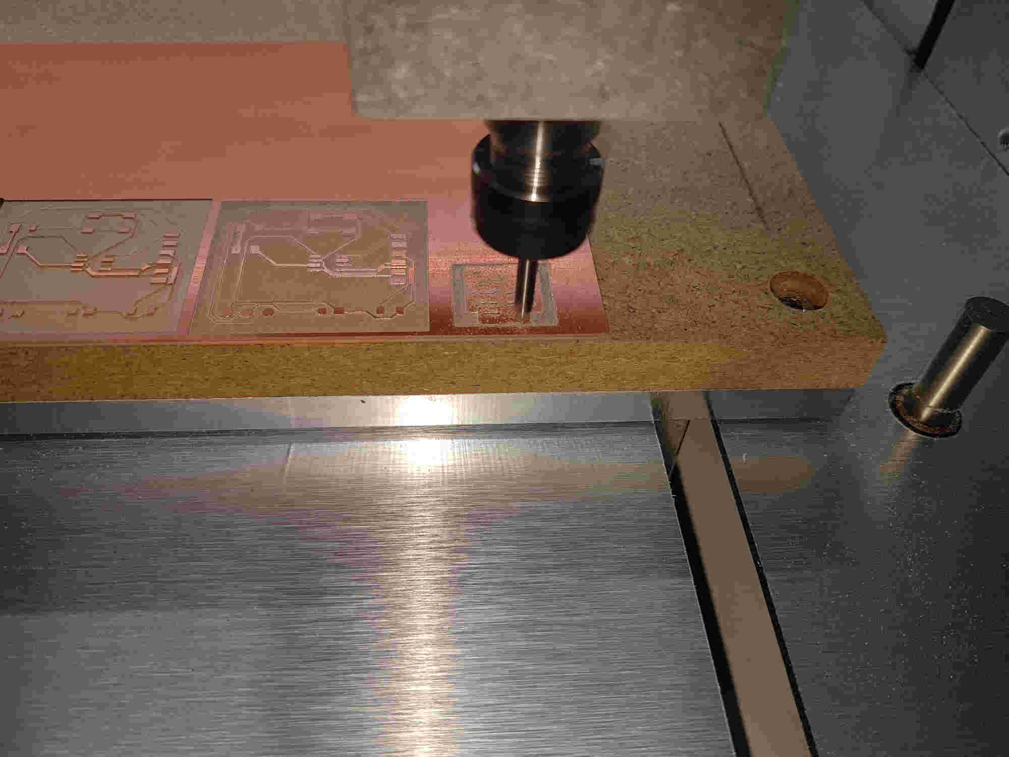
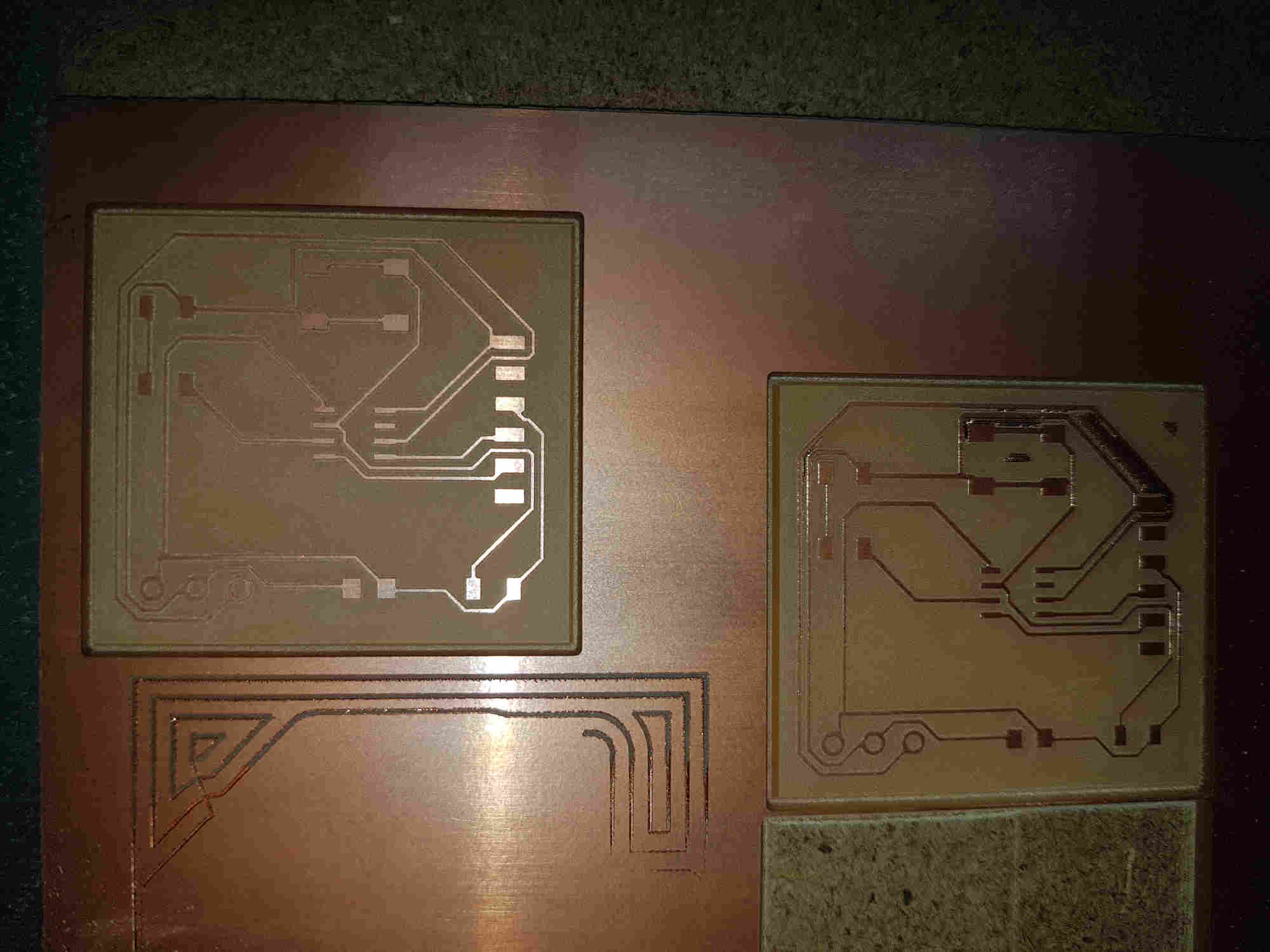
Cutting complete
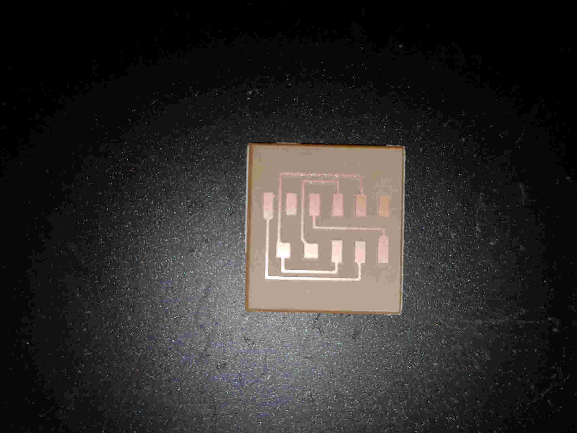
Now I had to gather the components for the PCB

Now my stress begins. Soldering the components
After sometime and patience I am complete

Download PCB board Carbide Create file
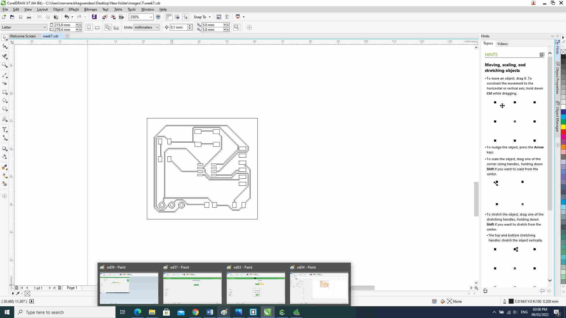
PCB process for Electronic Design
Import the Schematic week07.dxf file in Corel Draw . I made some additions edits to the board and exported to .svg file
Import file in Carbide Create , place/postion job ,setup the toolpaths and save g code

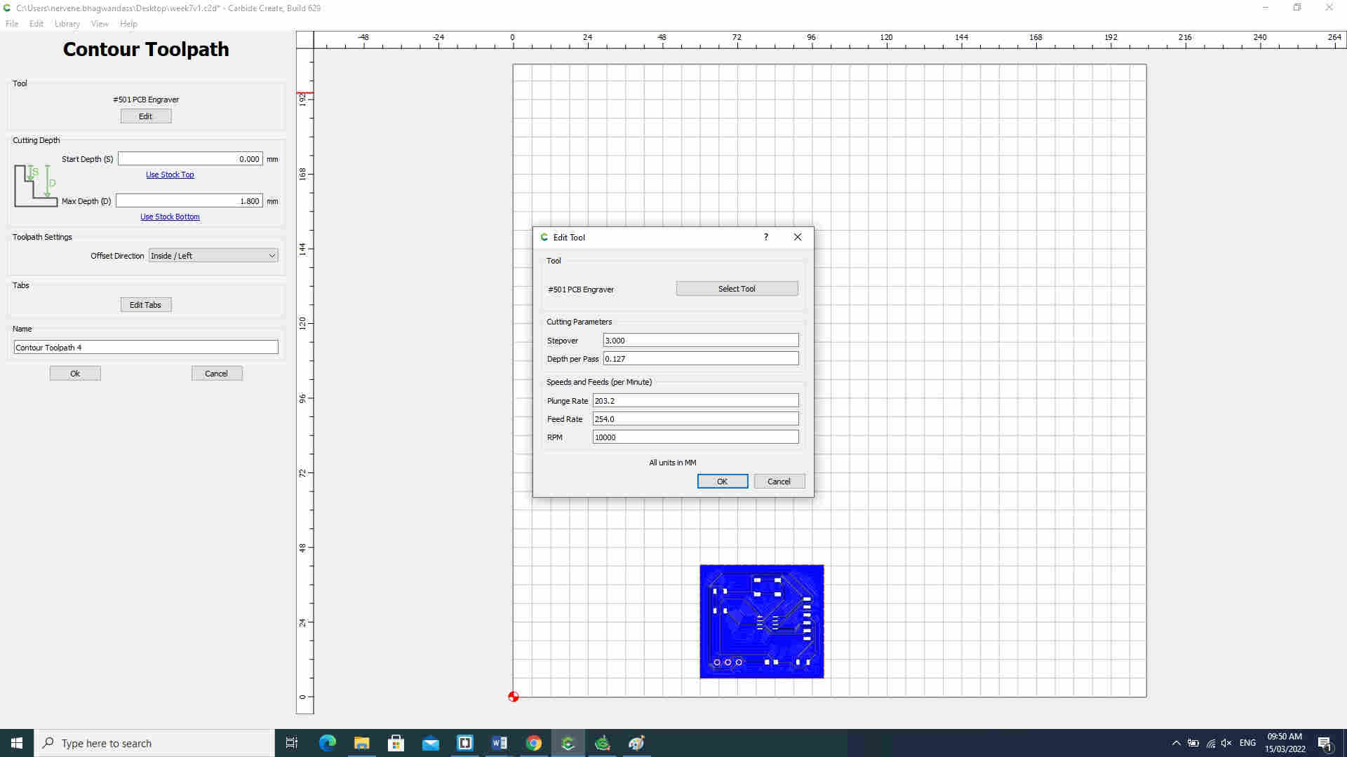
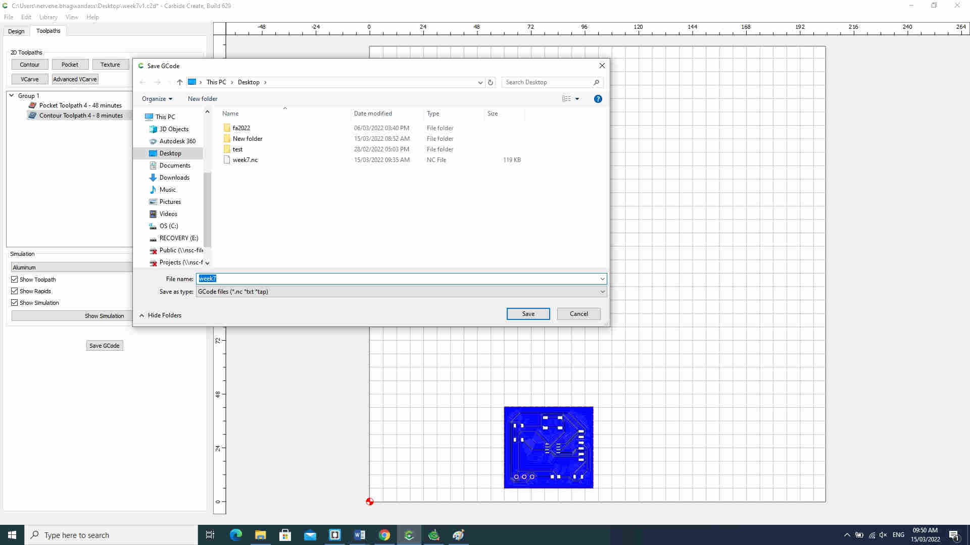
I connected to mill and went through the jog process in Caribede motion as previously documented in assignment 5 and then load week7.nc file
Milling and assembly!
I had some challenges dialling the pocket depth due the bit type and tracing width.
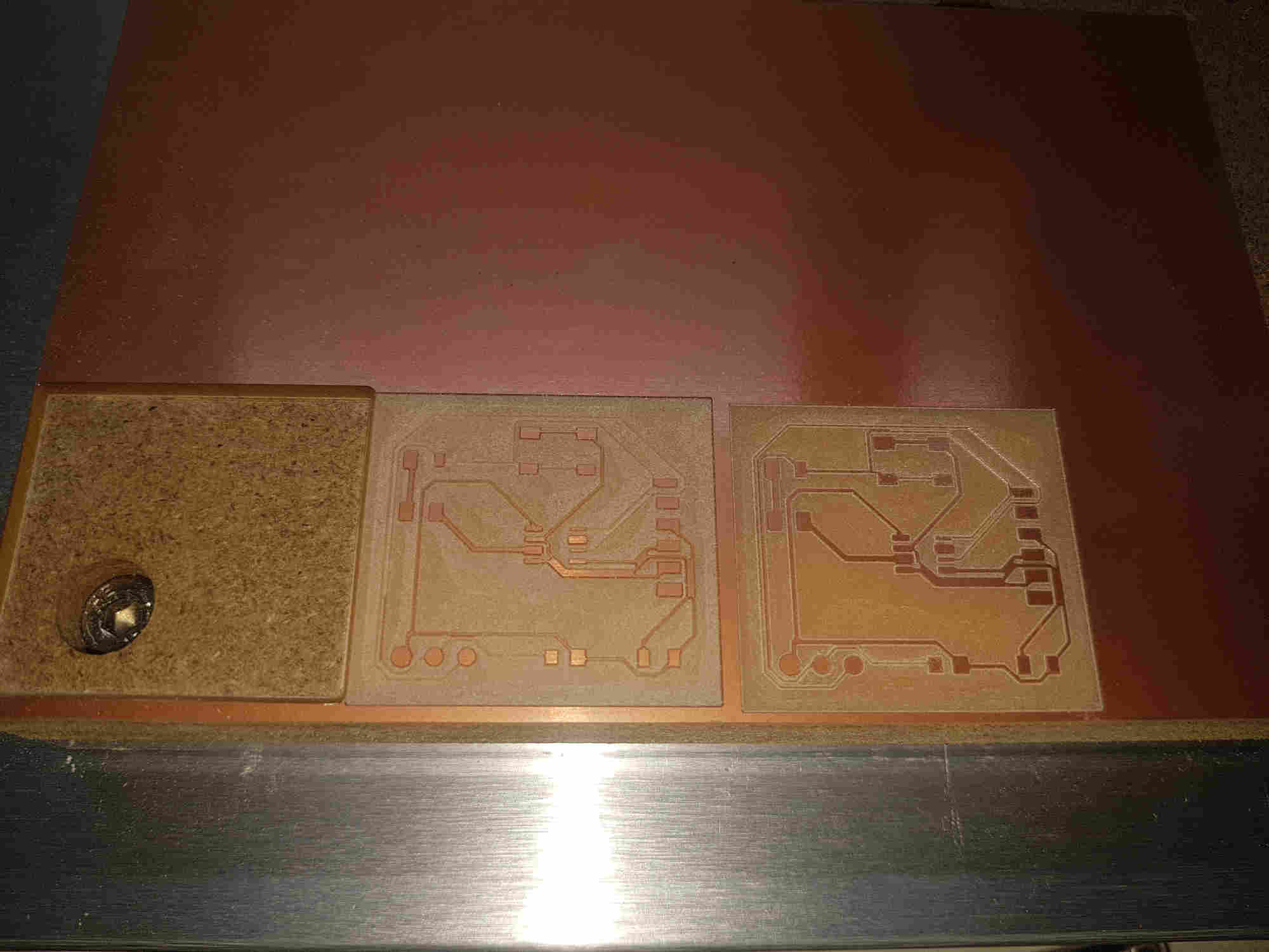
I corrected this by adjusting the tracing width ( making it wider) and pocket depth (decreasing the depth) I did get some success but it also highlight there can be defects in the copper board.
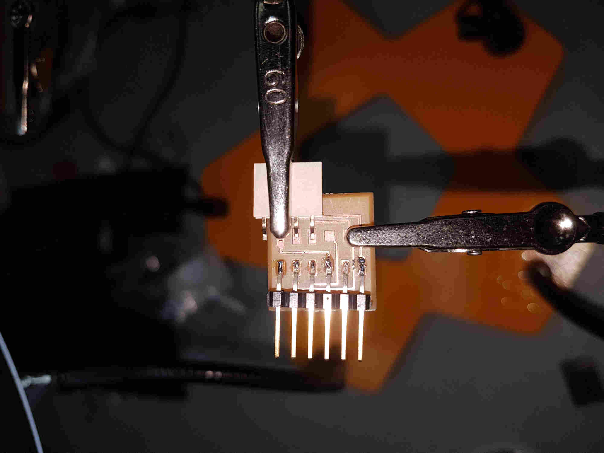
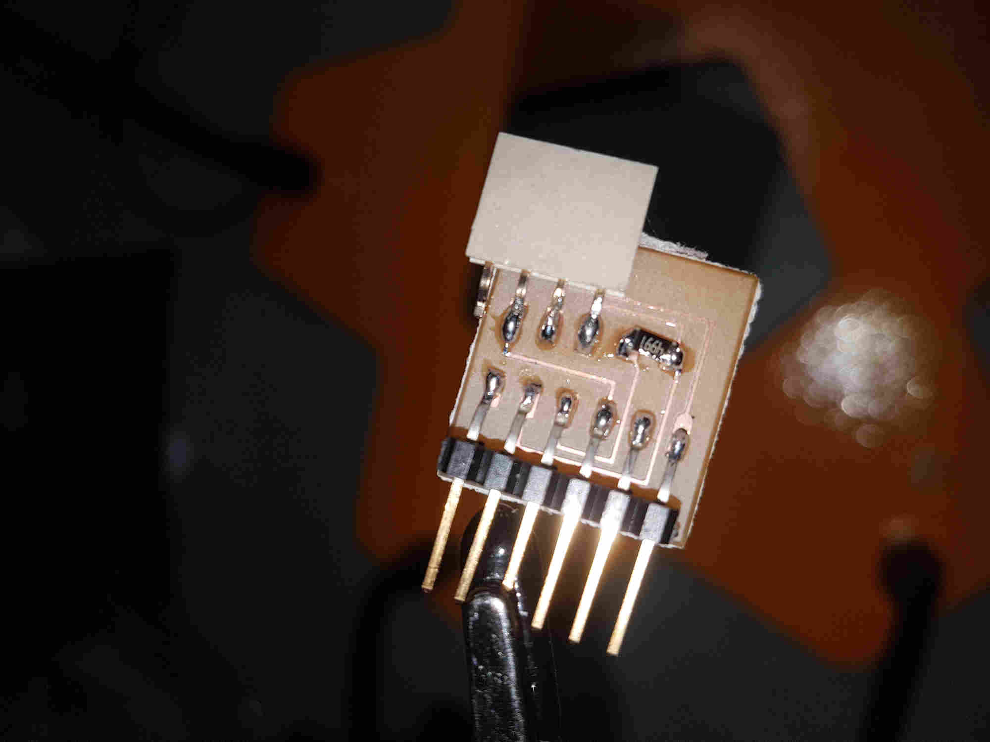
Soldering Circuit
I first located all the components for required for the PCB.

I then began soldering the IC Attiny 412 SSF to the board.
Note: Alway ground yourself while handling the IC
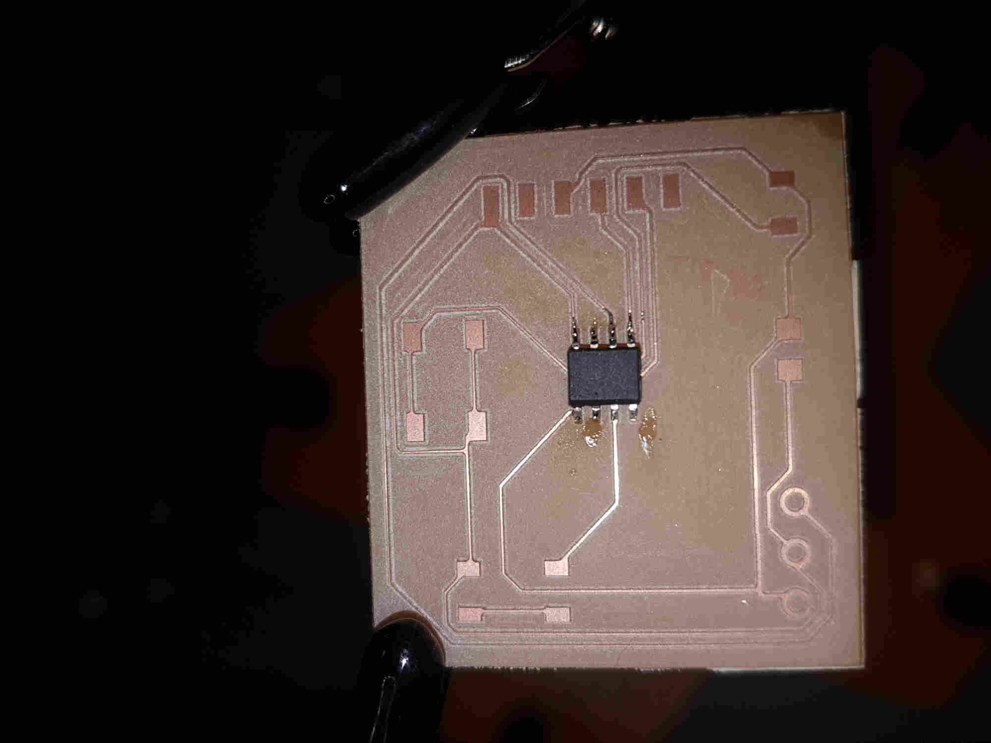
The other components followed.
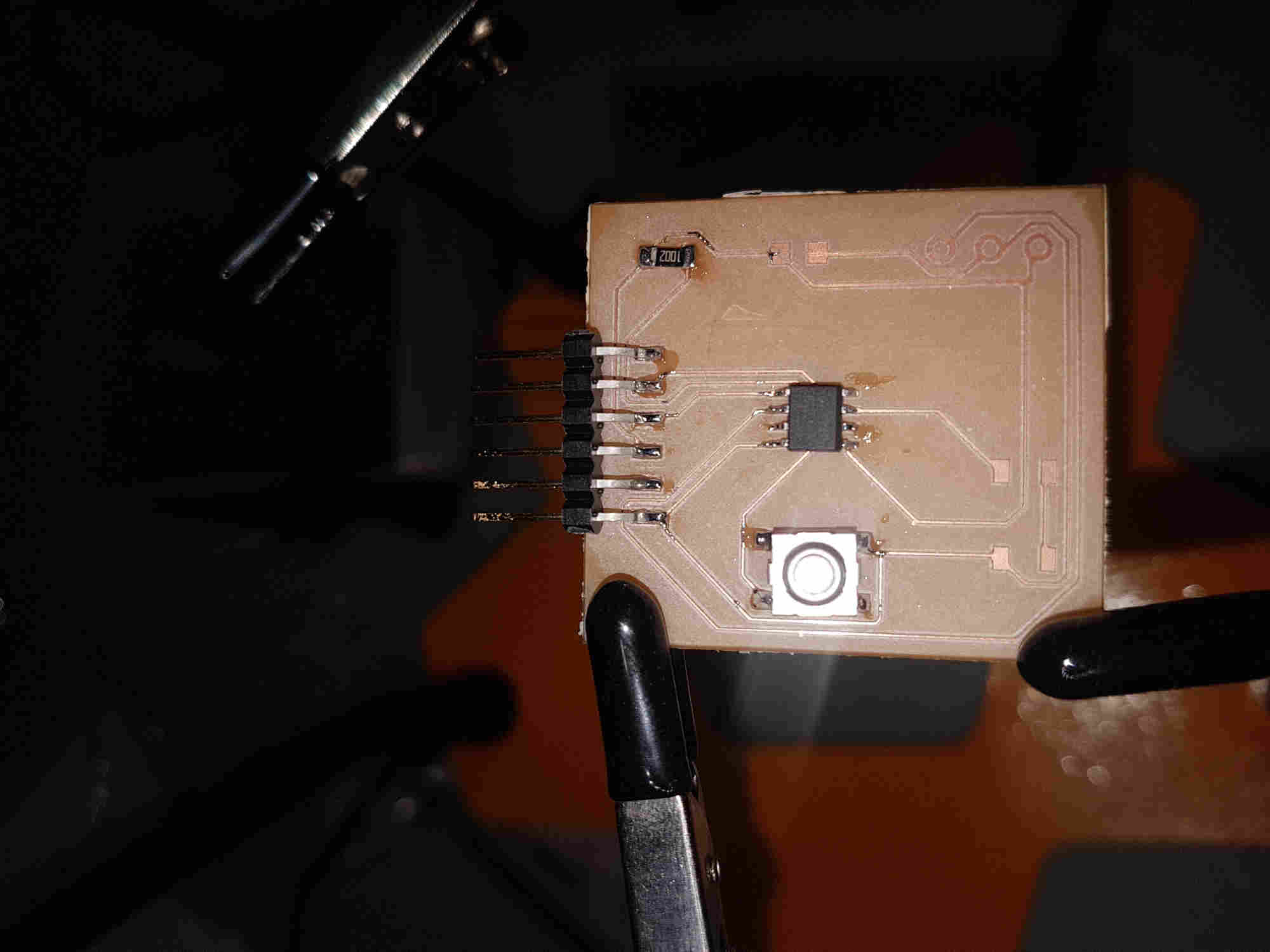
I completed soldering all componets