7. Electronic Design
This week, the assignment was to redraw one of the echo hello-world boards that we made in week05,with an additional button and LED, check the DRC for this board, make it, and test it. We also had to use test equipment to observe the operation of a microcontroller board’s circuit.
Individual Project
The individual project was to redraw the hello-world echo board, I will need to design, mill, solder, and program a board. Having taken engineering in the past, for the past few weeks I always felt like I had some knowledge of what I was doing, or some reference point to jump off of. This week I definitely didn’t do a lot of what I was doing until after I got into it, but I was able to produce a functional board and really understand the how/why that goes along with making a board.
Designing the board
We designed our boards in a program called Eagle CAD
I wasn’t familiar with it, so I watched two tutorials found here and here to familiarize myself with the software.
I decided to redraw the hello-board using the Attiny412 chip. I referenced the resources on the Fab academy page while designing my own board.
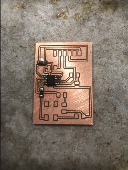
I actually ended up making two boards this week, because my first board had a lot of issues that would have made it unprogrammable. Unfortunately, I only discovered it was unprogrammable when I went to program it and one of my teachers saw it and said “hey, you do know you did this is all wrong, right?” So I included the information from my first board to give a better sense of my learning process with these boards.
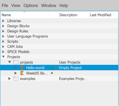
The first thing I did when designing my schematic for eagle was create a new Project under the Control Panel -> Projects tab. I then clicked it so the green circle would appear next to the project, telling me this project was “activated” or “in use.” I then right clicked and started a New schematic.
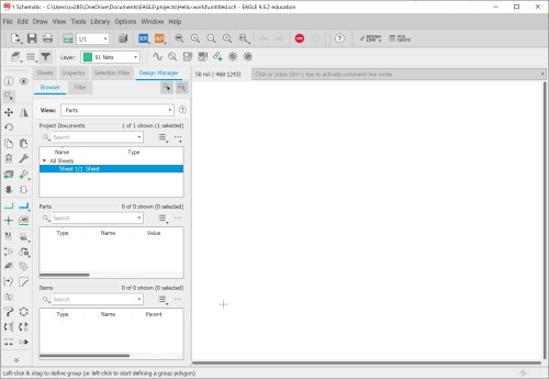
Schematic screen:
All the parts in Eagle come from component “Libraries,” so to make sure I was using parts that my local fab lab actually had, I downloaded the Fab Eagle library and a library specific to our fab lab made by our teacher Mr. Rudolph called Fab.new
To open them, put them under this path in your computer (replacing “USER NAME” for your username)
C:\Users\USER NAME\Documents\EAGLE\libraries
Back in Eagle, I selected the libraries from the control panel so they would have the “green dot” next to them meaning they were in use. To take parts from these libraries, I navigated back into my schematic screen and in the Search Bar typed the command Add. There is also a toolbar with this command as a button.
It brought me to this screen:
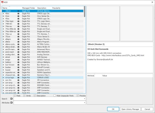
Where you can search for parts (make sure to include asterisks before and after your search string) or simply navigate through for them.
The parts I added(going off of my knowledge of circuits and Neil’s example board:
- Attiny412
- 6 prong pin header/connector
- 2 prong pin header/connector (for UPDI programmer)
- LED 1206 smd (surface mount diode)
- 330 ohm 1206 resistor
-
- Capacitor
- Multiple 0k jumpers/resistors (explained later)
- 10k ohm resistor
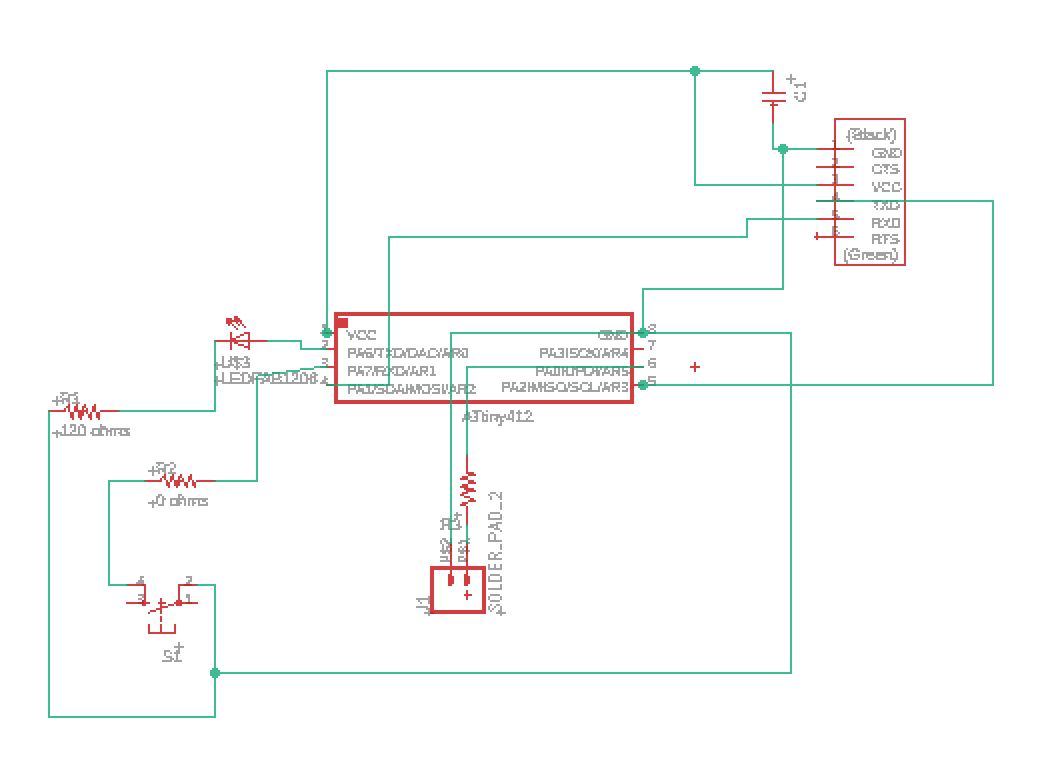
Here is an oversimplified description of my parts: The Attiny412 is a microcontroller with 6 pins as below:
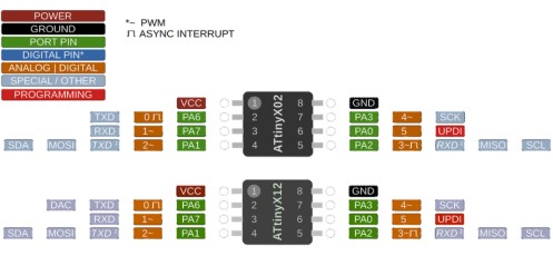
This chip is the “brain” of the microcontroller. It controls everything. It is also the powerhouse of an arduino. The pins are VCC (power input) Ground (return point for electrical charge) TXD and RXD (transmitters and receivers, one receives information and another transmits it. When connecting the chip’s pins to other things, like a 6 prong pinhead with TXD and RXD inputs, make sure the TXD goes to RXD and RXD goes to TXD< so transmitters are talking to recievers and recievers are talking to transmitters) UPDI (Universal programming and debugging interface, the pin that connects the chip to other things that can program it, and the SCK pin (for our purposes this was just another pin). What I have described are the “signals” of the chip, there are also things like MISO/MOSI (same pins, different use) but for my purposes this is what I used.
6 prong header: Like the above, has a VCC (power) Ground (electrical signal flows back here) a TXD and an RXD pinout. It has two more pins(obviously), however I just used them to connect to different parts. I needed to be able to connect to other programmers/devices etc. If the chip is the brain/controller of an arduino, these pins are simply all the pins around it. They are what allow your board to interact with other components outside of the board.
UPDI header: Another 2 prong pin, would be found on the pinout of an arduino. This one is simply used to connect specifically to other programmers/devices that can program it. (One pin connects to UPDI, the other connects to ground).
LED: it lights up :)
Resistors: 330 ohm: For my LED. It is a limiting current resistor. Calculated using ohm’s law. V=IR. Needed because: The VCC (power input) puts 5 volts into the circuit. These five volts flow along the wire, light it up, then flow out. The LED uses 2 volts, so 3 volts are still left flowing through the wires of the circuit, going back to ground. However, the amount of energy flowing back to the ground needs to be zero volts! So we need a resistor which will “resist” that extra 3 volts of energy, so by the time it reaches ground the energy is “0.” 5 total - 2 lost = 3 volts that need to be resisted. Substituting in: 3v = IR. I is current, which is.025 A. R that is needed is actually 120 Ohms, but we only have 330ohm resistors and higher, so I used that. (Resistance isn’t exact).
10 k ohm resistor: In between where the button meets the ground. We doesn’t want the current to flow out of the button and to the ground unless it’s absolutely necessary, so 10k ohms of resistance will make the energy flow anywhere but there unless the energy absolutely needs to go back to ground.
Capacitor: Almost like a battery. Holds a certain amount of charge. Needed later for the programming.
0k Ohm resistor: Needed for jumping over traces on my board (described in more detail later).
After I placed all my components I connected them with the net tool. These nets are going to function as the “traces” of my board, which act like wires but are engraved into the copper. I later found this series of tutorials which I didn’t find until after making my board but had a lot of useful information.
After placing all my components I “wired” them together using the net tool. Unfortunately, I didn’t understand any of this when I first made my board. In my original schematic, I was able to look at enough pictures of boards to sort of know where each one needed to be. However, I didn’t understand the concepts I described above until later, So in my original schematic, the errors I had were as followed:
The UPDI: needs to go to UPDI pin on attiny and ground. Mine didn’t go back to ground, or to the correct UPDI pin. The capacitor didn’t go back to ground. I didn’t really understand the concept of ground yet. And the TXD and RXD attiny pins needed to go to opposite TXD and RXD pins on the 6 pronged programmer. They didn’t connect, I didn’t know what they were yet.
My schematic got a lot better after surfing the internet/ talking to my teachers. Here is the final:
There was also a lot of back and forth in my head and with my peers as to if we needed a resistor on the switch (not for the ground, coming right after the pin leg) for programming. Because I used a pull-up resistor (which I will describe later) I did not need to do this.
I also took this opportunity of remaking the board to clean up my Schematic a bit. The capacitor was supposed to be next to the VCC leg of the Attiny. Also, I had already routed and soldered it, but was afraid my 6 prong pins might be too close to some other traces and I was afraid there might be some overlap. I had planned to test it with a multimeter anyways afterwards to make sure the only connections I have are the ones I’m supposed to have and I don’t run into any problems, but this won’t hurt so I did it anyways.
I ran an ERC, which is an electrical rule check, to see if I had any glaring errors with my electrical diagram. It doesn’t tell you things like “hey you need to connect TXD and RXD, and make sure everything is connected to the same ground,” but it did tell me I needed to assign values to my resistors and a few other parts.
At a certain point later while troubleshooting and re-checking connections, I was told the value tool can name traces on schematics, and then when you switch to the board and click on the trace the value of the trace will appear, which was helpful!
Design file for Schematic (follow link and then download)
Making the Board
I then switched the schematic to a board using this button:
The first time you do this, the schematic will make a board. Every other time, you will just be switching back and forth. Changes you make in the schematic will propagate to your board in what is called forward/back annotation. So changes made in either will be transferred to the other one.
Board Screen Layout:
After rearranging my parts, I used the Air Wire tool to route my nets from my schematic into actual traces. You simply click on your component, then continue to click until you reach the part you want to guide it to. The traces appear in yellow to help guide you in the background, then disappear once you have finished making a connection. You can also use the Auto-route tool, which I tried at first, but I found this to be difficult to change manually, so the few places I wanted to change would require me to change the whole board. So I chose to do manual routing.
There were a few places I used 0k jumpers/resistor because my traces would have crossed each other. 0k resistors/jumpers do absolutely nothing, they just allow you to place a component over a trace. At first, I spent a really long time trying to mitigate the amount of times I used these resistors, but I ended up using quite a few.
DRC
I ran a Design Rule Check (DRC) for the specific mill we are using, the Other Mill Pro by Bantam Tools. All DRC’s are is a set of rules you must follow to make sure your board is actually millable on your tool. There is a written out version of the rules which you can check manually, but running one is much faster. Other Bantam information on Eagle can be found here.
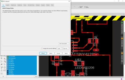 (hit check to run all design rules. Problems will appear in a popup to the left. If you have no issues, a message confirming no errors found will display in the very bottom in a white bar that is already there, so is hard to notice.
Mine told me I had lots of airwires sticking out in random places under component pads. I must have accidentally clicked too many times. I fixed these.
It also missed a couple of traces that were too close, but showed up in Eagle, so I had to go back and space them out a bit.
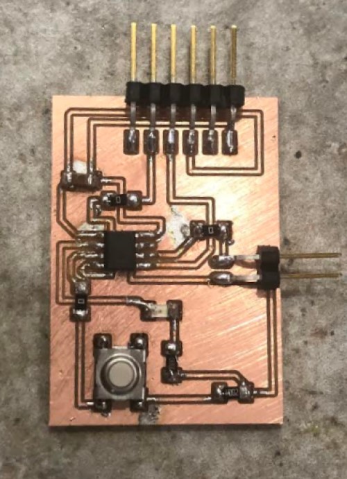
Final Board:
Design file for Board (follow link and download)
Milling
After routing all my traces, I milled the PCB. I first tried to take a photo of the top layer only and open it in Fab Modules to make a toolpath, but I later found the easiest thing to do was to simply open the file in Bantam Tools twice, make the traces invisible in one file (once already opened in Bantam) then make the outline invisible in the second, and mill both straight from there. (red For more information on steps for milling, refer to the Week05 Electronic Production week05
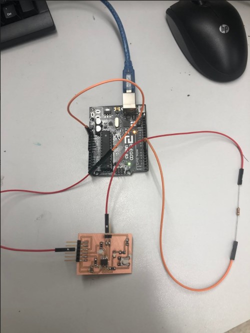
Soldering
Once I milled the board, I soldered all the parts together.Surface mount Soldering is something I am relatively new to. I tried it in week5 and I wasn’t entirely pleased with my craftsmanship. You can find a lot more detail on my soldering process there too. However, I got a lot more practice this week and my board turned out much nicer.
I started with the Attiny, then worked my way out. I did the pins last.
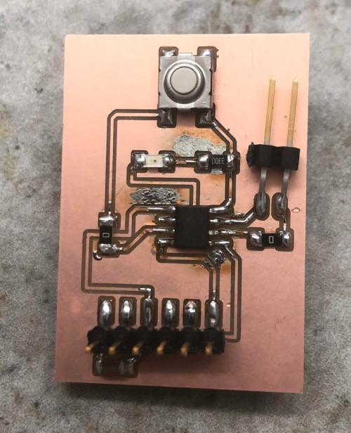
This photo shows places where I had solder bridges, and when I used a wick to remove them I was left with a lot of solder stuck to the very bottom of the board. It doesn’t affect the board, but it isn’t very pretty either.
Final Board:
You can also see the board I originally made after I finished soldering for comparison:
I think the actual final board is soldered a lot nicer.
Programming
Trying to program really threw me for a loop. I knew I needed to program my board so the UPDI pins were usable, then use those pins to test my programmer with an echo code.
Setup:
I began following the video tutorial below to program with arduino. The video referenced parts of this project on Github, though as I explored it more I realized this user has made a near complete guide on everything I needed for this week which I found very helpful.
Originally I used an arduino in my setup, like the video tutorial instructed. When we upload code to an arduino it goes to the chip. The chip will reset it’s code when the arduino is turned off(which is does whenever code is uploaded through the ide), but if the code is wiped and the arduino turns off, then when we try to send code through the arduino to my board, it will be sent to the arduino.
To stop this from happening, we attach the reset pin to the capacitor so the “battery-like” capacitor passes it’s stored energy to the pin, keeping it on temporarily.
However, Dr. Harris showed me a clever workaround for the Arduino that gets rid of the “Reset” problem. IT used an FTDI chip. I decided to go with that because I couldn’t actually figure out what capacitor to use, all the sources I was using disagreed on what to use, and further research didn’t help. So I tried that.
In the setup for that, you need both the FTDI and my board on the same 5v energy pin on the arduino. Otherwise, the TXD goes to the RXD pin (and vice versa) and ground goes to ground to the ground (on my board. Pin 6 of the arduino still goes to the UPDI port
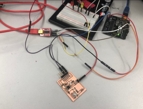
However, whenever I tried to use this setup my code would simply “Upload” forever on the Arduino IDE, so I switched to using a different programmer board. This had the same setup as with the FTDI chip and the Arduino, but it didn’t have multiple wires all going to one 5v pin.
The Code:
To get the ATTINY core downloaded, I went through the installation and programming guide of this site. The wiring guide was also helpful, but I had already done my wiring so I just used it as a check. I disregarded the capacitor information.
I uploaded the board manager code to Arduino through Arduino IDE. I followed the steps on the github repository with the ATTInyCore Code. I had to go to File -> Preferences and copy the board manager url to the “Additional Boards Manager URL” field. To open it, I think navigated through Tools -> Boards -> Board Manager, then
“ File -> Preferences, enter the above URL in “Additional Boards Manager URLs” Tools -> Boards -> Boards Manager… *If using 1.6.6, close boards manager and re-open it (see below) Select “ATTinyCore by Spence Konde” and click “Install”. ”
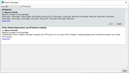
I then went to Tools -> Board and tried to change the Attiny core to the Attiny412, but I found out I had actually downloaded the wrong TinyCore package. You shouldn’t search for “ATTinyCore by Spence Konde, just search keywords until the second option appears, then download that.
You also need to open a special .ino file, this will be the code that programs the UPDI pin as a programmer. Once you have installed and extracted these downloads, navigate into the “Source” folder and open “Jtag2UPDI.ino” If the file folder it is hosted in is not named “Jtag2updi” then it will not open. I then went back into Tools -> chip and selected Attiny412 and set my programmer to jtag2updi (megaTinyCore) under Tools -> Programmer. When I ran the code it seemed to upload. I then ran a blink code, and it worked!
I then ran a code so that the button would be part of the code. I loaded the basic button code on Arduino, but I needed to include a pullup resistor. With a button, you typically have a button connected to pin and the ground. When the button isn’t closed, the pin state is technically “unknown.” This is because it doesn’t connect back to the ground, the wire is just floating, like an “antenna.” So that we have a state of certainty all the time, the pin with the button is connected back to the VCC. This is already done inside of the chip, so I didn’t have to do anything on the hardware side. This gives it a constant state of being on (high.) Since it is always high, we need to change the software so a “Low” state (when the button is disconnected) is what will turn the button on. However, we also have to consider that having the VCC go straight to the button will short it out, so we need to add a resistor between the VCC and button pin. Since it is inside the chip, it is a “pull up” resistor. So I opened the example code for an analog button on arduino, and edited it to refelct the changes above by changing the following: Changed “pinMode(buttonPin, INPUT);” To “pinMode(buttonPin, INPUT_PULLUP);” and, I set the button state to 0 (meaning the button will be low when not pressed) and switched the output statements. Originally it was written so when the button state was high, LED would be low, and vice versa. But with a pullup resistor, said when I uploaded the code. It worked!
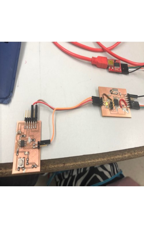
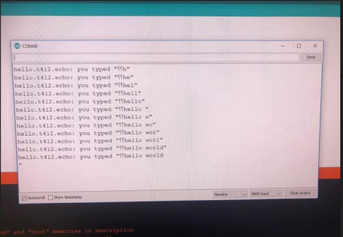
The last thing I did was upload Niel’s Echo code to the board.
The only change I had to make was to change the line after “Serial Begin” to 5600, and changed that to be reflected in the baud of the serial port monitor. If you don’t do this you get gibberish. You also get gibberish if you plug the board in the wrong way. You can open the serial port monitor by going through Tools -> Serial Monitor. Once you have uploaded the code, remove the programmer and plug the board in directly to the com port (FTDI chip). Type “Hello World” into the Serial Monitor and you will get the following back, showing the board was able to send data, receive it back, and display the data it receives! (echoing it!)
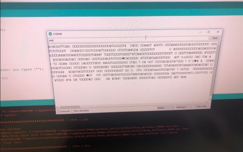
Some fun gibberish:
Echo:
Group Project
This week’s group assignment was to use lab equipment to observe the operation of a microcontroller circuit board. We split into smaller groups, and heavily focused on using an oscilloscope, which none of us had used before. We used it to characterize the waveform of an arduino. Our group project page is here
We started this week learning how to use the SDS1000X&X oscilloscope. An oscilloscope is used to analyze the waveform of electrical signals. We tested ours on an arduino running a blink code. To learn how to use the oscilloscope, we referenced the user manual and ended up following this tutorial. It was also recommended to us that we watch the video below when we were starting off.
We are using the SDS1000X-E Series oscilloscope by Singlet.
To set up the machine and calibrate the machine, we first uploaded the blink code and put male jumper cables in the 13th pin and the ground pin. We attached the oscilloscope probe to the “X” port at the bottom, and attached the clamps on the probe to these cables. There are a number of settings the oscilloscope needs to be on. Make sure Channel 1 is on, Channel 2 is off, it is set to DC coupling, Set the Probe attenuation to “10x” (done with a switch on the probe, and by adjusting the attenuation on the Oscilloscope itself) and under the trigger menu, the trigger type is set to “Rising Edge” and the Trigger is in “Auto” mode.
The waveform should appear on the screen.
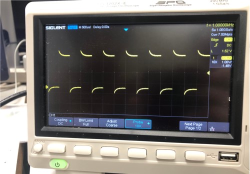
The wavelength still needs to be fixed, however. It needs to have a flat top, or be “square,” which you can do by using a mini screwdriver and tightening a mini screw found on the probe. To “zoom” in and out of the wavelength so it fits the screen, change the vertical and horizontal knobs.
This waveform shows the voltage reading across the screen. It alternates between it’s high state and low state as the LED is turned on (High) and off (low).
This, however, is not the only way to measure voltage or characterize an electrical board. We also prodded around the arduino with a multimeter, a tool that we often use to check connections while soldering. It will show you if lots of things are flowing, like voltage, current, and resistance are flowing, and will give you specific values where applicable. It functions by completing a circuit so it can measure whatever energy is flowing from point A to point B and/ or send current through the points at one probe to see how much comes back at the next (By point A and B I mean the places where the multimeter probes are on the circuit).