Electronics Design
Soldered board

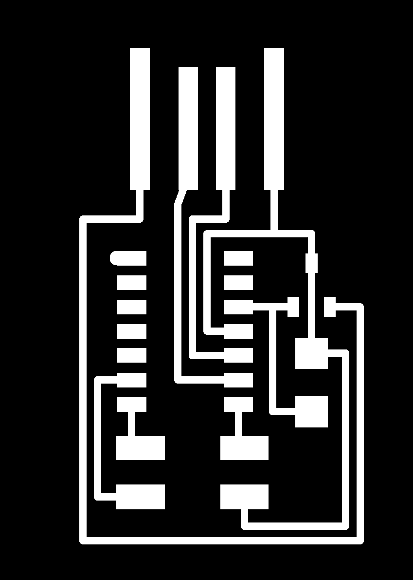
Concept

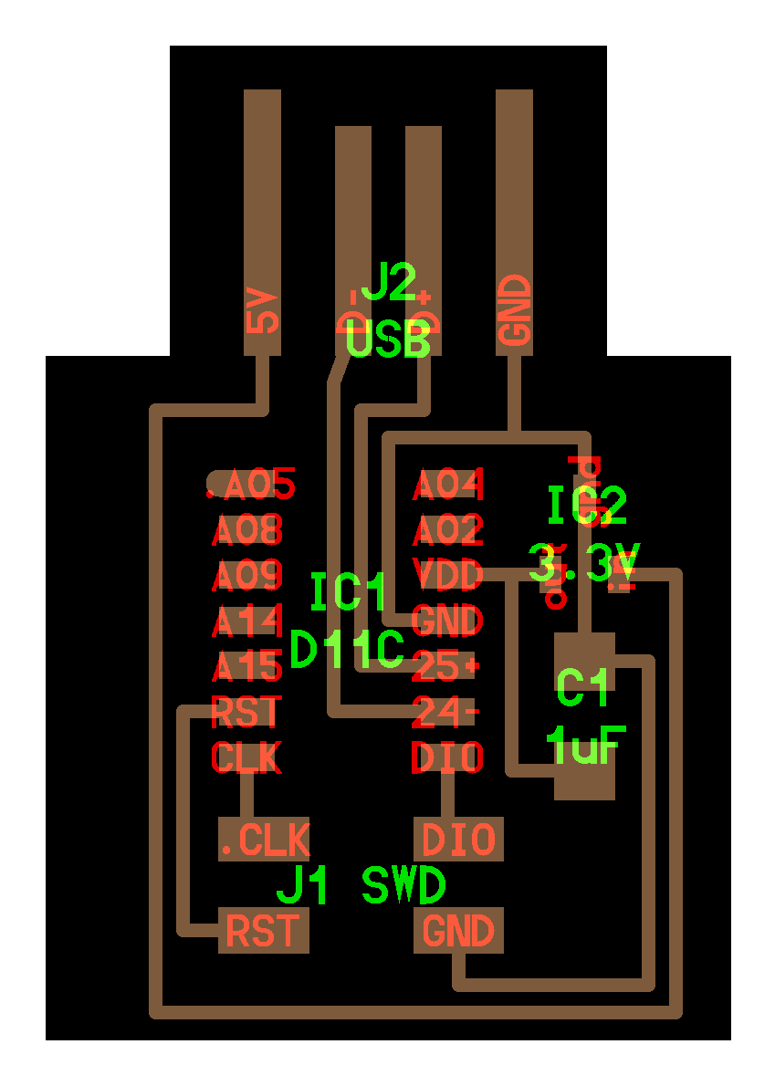
Components Diagram

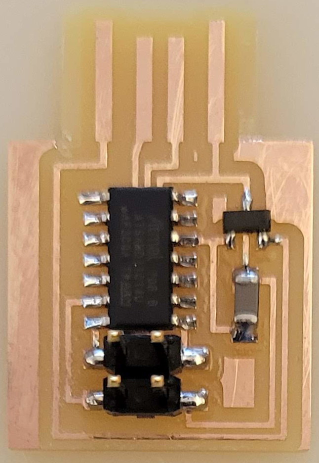
Milled board

individual assignment
- redraw an echo hello-world board ✅
- add (at least) a button and LED (with current-limiting resistor) ✅
- check the design rules, make it, and test that it can communicate ✅
- extra credit: simulate its operation ✅
The initial approach for this week was to replicate, and then customize, the ATSAMD11C D11C-echo-4 pin sample board.
Sample Board
Traces
Components
Finished sample board
Getting setup with KiCad
Just like the rest of the Barcelona gang, I chose to use KiCad for my first board. I’ve read that Fusion360 has support for board design and manufacturing, but I wanted to try an opensource tool that worked well in Linux, which is what I use in my daily driver computer.
tl;dr: Check out known issues when upgrading from KiCad 5 to 6
After getting setup with KiCad 6, I had to install additional libraries for the components that we have in the FabAcademy Electronics Lab.
This library (and footprints) is available in the fabcloud gitlab and allows us to easily reference electronics components that we will likely be using for most of our build (their references, their sizes, their footprints, etc…)
Workflow
Drawing the board

- Draw the board with pen/paper
- Select which features you will need
- LEDs, buttons, etc…
- the microcontroller has already been picked for us
- Design a first iteration
- Calculate the features of the components that you want to include
- Resistors, Capacitors, etc…
- You will need to know what’s available in the lab, and find the datasheets for all the components
- Select which features you will need
Creating Design in Schematic Editor

- Draw the schematics (initial sketch) in KiCad
- The Schematics tool in KiCad can be used to insert all the components you will need, and the general connections for each of them
- you don’t need to do the overall wiring during schematic design, you will do that later.
Configure Design Rules for KiCad - Net Classes

- ⚠️ Before you do anything, configure the design rules and constraints for your PCB
- You can do so via the menu: File => Board Setup => Edit Pre-defined Sizes => Design Rules => Net Classes
- Standard settings for the Roland SRM-20 mill we have in the classroom are:
- Clearance: at least 0.4mm (distance between 2 paths)
- Track Width: 0.3mm (for low voltage tracks)
- You need to do these before you start drawing the traces, so that the software can help you with boundaries, sizes, and clearances.
- If you forget to do it before you get started, there’s a workaround to retroactively apply these settings to traces you have already defined:
Creating the traces and board layout
- Once you’re happy with schematics move the design to the PCB Editor
- In here you will be able to design the traces and paths for the actual PCB.
- Draw the traces between components
- Export as SVG
Inkscape
- Inkscape - final prep for ModsProject
- Use Inkscape to draw the outline for your board.
- Prepare your traces file so that they follow Mods guidelines (black = to be milled, white = to be kept)
- Save as PNGs
Produce the Board
- Follow the steps
from 2 weeks ago (Electronics Production) to produce
the board. Use ModsProject to create the toolpaths for your milling tool
- Remember that you can use the customized programmes for the Barcelona milling machines
Lessons learned
Workflow management and structure
The main pitfalls this week were around:
- Workflow management: Lots of gaps in knowledge and the standard workflow meant that we had to repeat the design, draw, mistake, re-start loop multiple times.
- Basic electronics skills:
- How to calculate the required resistor for a given circuit/path so that the LED does not burn,
- What’s the optimal way to connect a button to a microcontroller, so it can measure its state (Pull-up v. Pull-down resistors)
- How to navigate electronics databases/specs:
- Where to find datasheets for components, and how to read them to find key bits of info.
- How to find the models/libraries/footprints for components so that they can be included in our designs.
Problems after upgrading to KiCad 6
Migrating from KiCad 5 to 6 caused some problems with libraries
Running dpkg --list from the terminal shows that there are some leftovers from previous versions

This set of commands cleaned up my laptop from leftovers from KiCad 5 and allowed me to install KiCad 6, with its recommended dependencies.
sudo apt-get remove kicad
sudo apt-get remove kicad-doc-en
sudo apt-get remove kicad-footprints
sudo apt-get remove kicad-packages3d
sudo apt-get remove kicad-symbols
sudo apt-get remove kicad-templates
sudo rm -r -f ~/.config/kicad
sudo add-apt-repository --yes ppa:kicad/kicad-6.0-releases
sudo apt update
sudo apt install --install-recommends kicad
Soldering and De-soldering
During the soldering process this weekend, I came across a problem that I didn’t know could happen.
The thin layer of copper god peeled off the board while I was trying to solder one of the components.

Can you see this? This is one of the 0.3mm traces (between the USB and the microchip) that got stuck to the solder.
🌈 Time to start over ✨
Next attempt: the same, but with a copper pad.
The tiny shiny copper square should not be laying on the gray soldering mat.

This has resulted in a small setback since I don’t know how to fix/restore the board. The only was forward that I can think of right now is:
- De-soldering everything off of this board.
- Go to FabAcademy on Monday and mill a new one.
- Start over.
- Fail again.
- Fail better.
Learning to de-solder properly would also be a useful skill to master

While I was de-soldering the microprocessor from this board I was too eager to get it off and I accidentally peeled off one of the data traces.
In any other circumstances, this would also have been a board-breaking problem. In this case, since the board was ( probably) not recoverable, it’s a valuable lesson, at a discounted price.
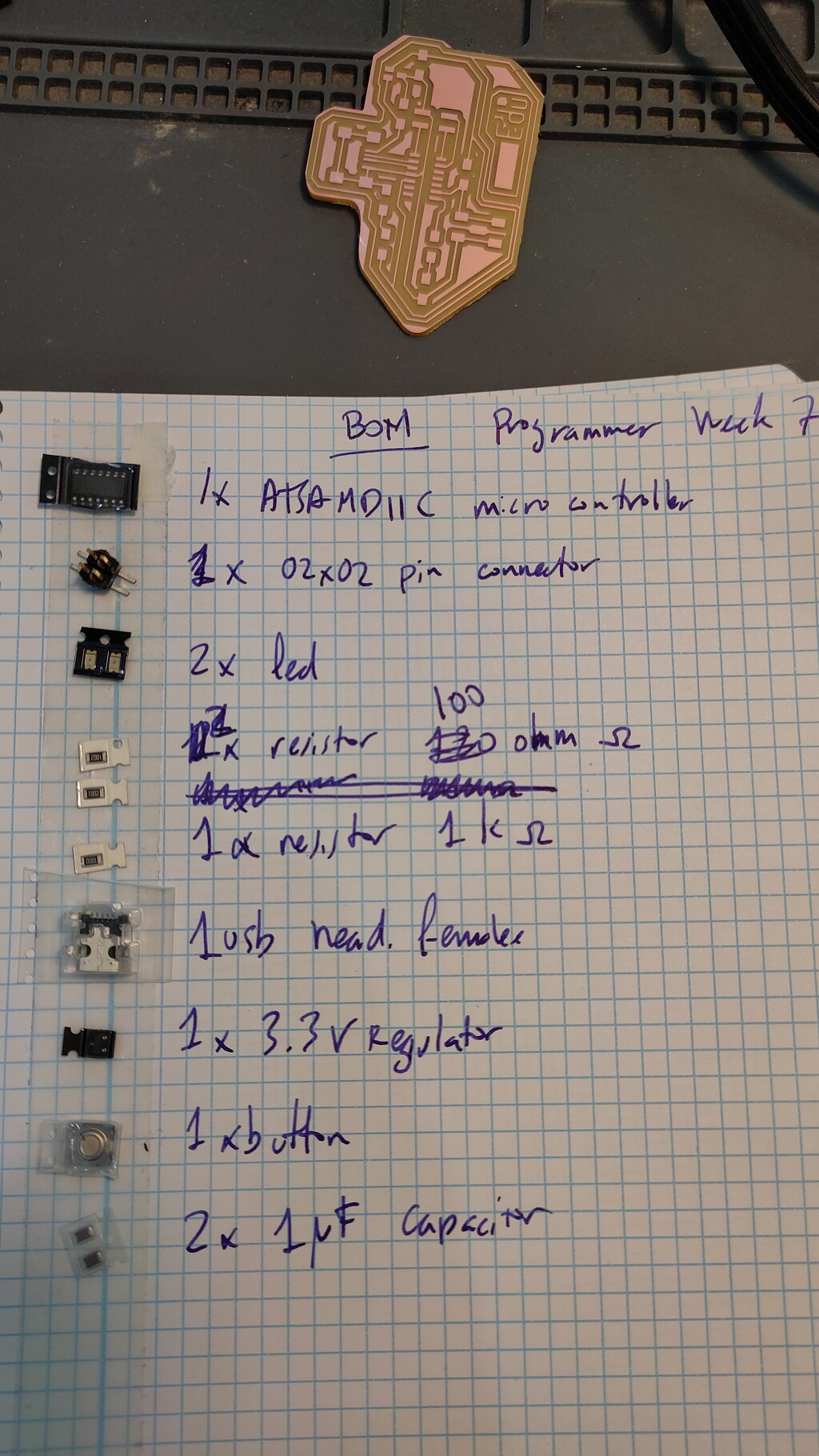
Bill of Materials
| Qty | Element | Purpose |
|---|---|---|
| 1 | ATSAMD11C14A Microcontroller | Programmable microcontroller |
| 1 | 02x02 male pin connector | 4 pins for SWD programming |
| 2 | White Difused LED | 1 to indicate if the board is powered, 1 programmable output |
| 2 | 220 Ohm resistor | Protect LEDs |
| 1 | 10k Ohm resistor | Pull down resistor for button |
| 1 | Mini USB Female port | Connection to our PC so we can program it without SWD |
| 1 | 3.3V voltage regulator | Regulate 5V from USB to 3.3V that the chip needs |
| 1 | Button | Programmable button to receive user input to chip |
| 2 | 1 µF capacitor | voltage regulaltor requirements, stabilize current |
2nd attempt
The second attempt for this assignment only involved execution tasks.
The original design was fine, so it was just a matter of printing a new board and getting down to solder again.
A couple of tools that really helped me in this soldering session were:
- The lens with a x10 magnification factor that we have in the lab. It allows me to check tiny details without straining my vision.
- The thin tip for the soldering iron: this week we got new soldering tips for each of us. It was great to be able to solder at home without having to bring the heavy bulky ones. The only issue is that the thin tip died really quickly (the thin material disappeared and after a couple of sessions, it’s as thick as the normal tips).
In our next episode…
Do you think we will be able to finally master the art of soldering?
You will have to wait until week 08 to find out!
Spoiler alert! 🤯 We ended up milling 8 copies of the same board during that week… so the outlook is not looking great!
Here’s a short story/famous quote about persistence that has helped me throughout these weeks.

Credit: illustration by zenpencils.com, story/quote by Calvin Coolidge
Assets
- thirdboard.zip - KiCad Design (zipped)
- traces-helloworld.rml traces file
- outline-helloworld.rml outline file