Cheatsheet: Creating a Custom KiCad Footprint
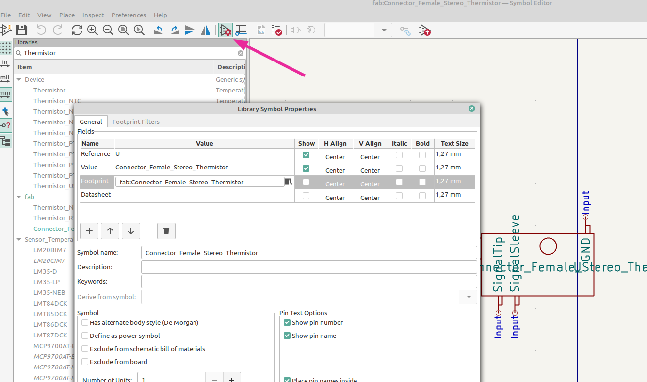
- Go to Symbol Editor
- Find the library you want to edit
- Create new Componennt (right click)
- Give it a name

- Draw the Symbol
- The sizes and proportions don’t actually matter.
- You just need to make sure you mark which inputs the device will have
- Remember to number the pins so that you can later reference them in your footprints

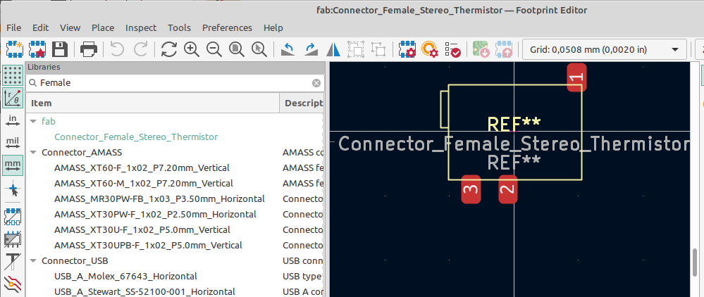
- Go to Footprint Editor
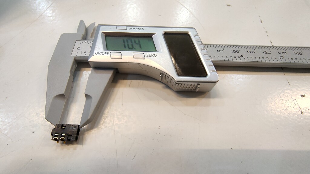
- Design the Footprint with the measure that you have taken
- Make sure to add pads at the correct positions, and that you are using the correct design rules so the pads have the appropriate size.
- Also make sure that the pad numbers match between the Symbol and the Footprint, otherwise you will have serious issues when you try to from Sketch design to PCB Layout Design.
- Include the design to your Sketch
- From there, you can assign a footprint to the symbol if you double-click on it.
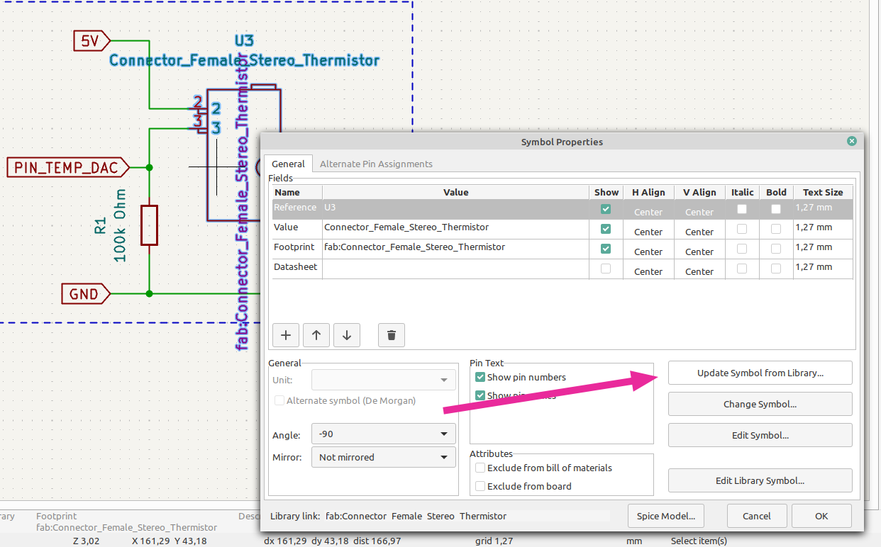
If you are getting errors after you made changes to the design or footprint, remember to do an “Update from Library” so
it picks up the latest changes on your sketch file
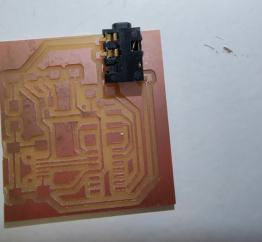
If you did everything correctly, you should see these lines on your PCB design, indicating that all the configs are correct and that KiCad expects you to design the traces for those lines
Nothing beats the satisfaction of seeing that it went well on the first try: