7. Electronics Design
Week Assignment
- Test the operation of a circuit board (group).
- Design a hello-world board with additional buttons and LEDs (individually).
Design a Hello-World Board with Additional Buttons and LEDs
I designed a hello-world board using an ATtiny1614 with an additional LED and button. The design process involves three main steps:
- Defining the schematic
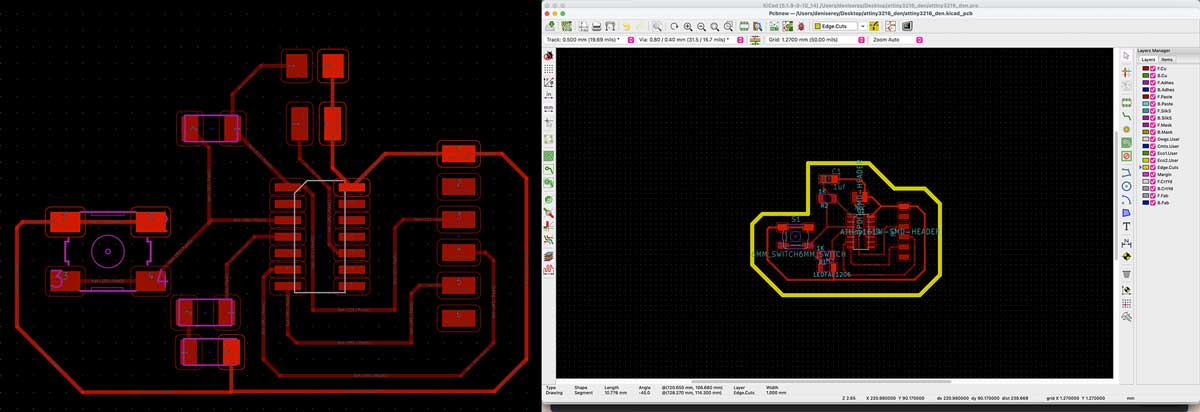
- Designing the PCB with the traces
- Building the PCB
As we were introduced to KiCad during the class, I used the ATtiny1614 datasheet as a base for my design.
Example ATtiny1614 Board
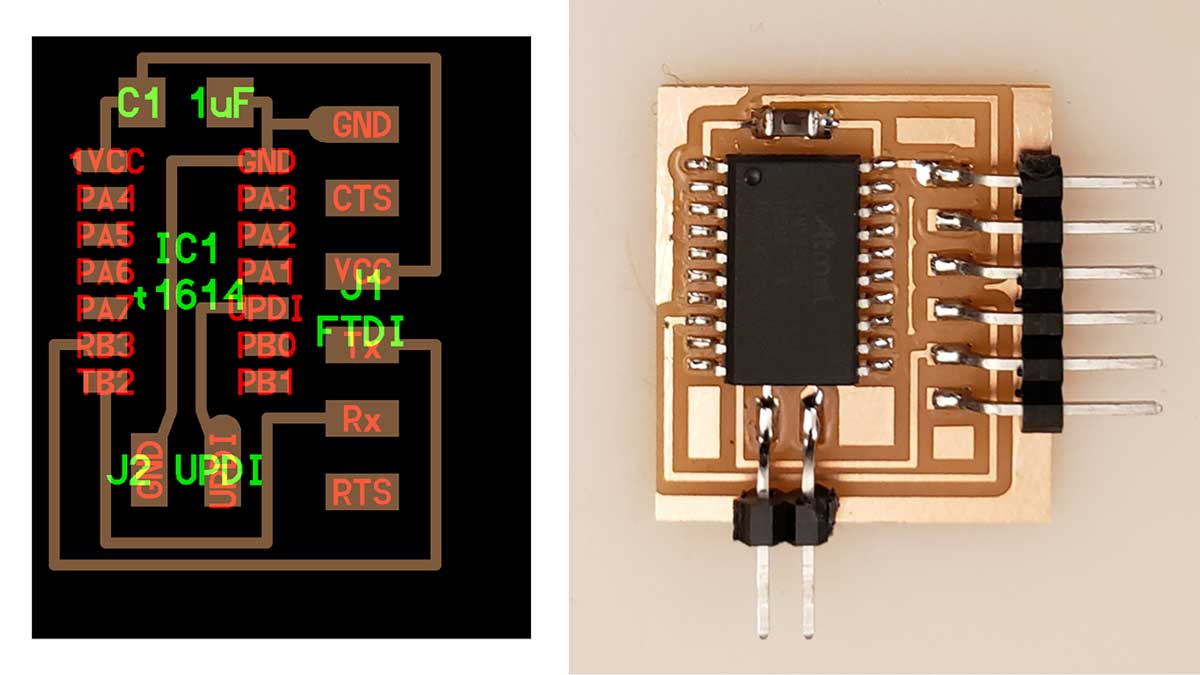
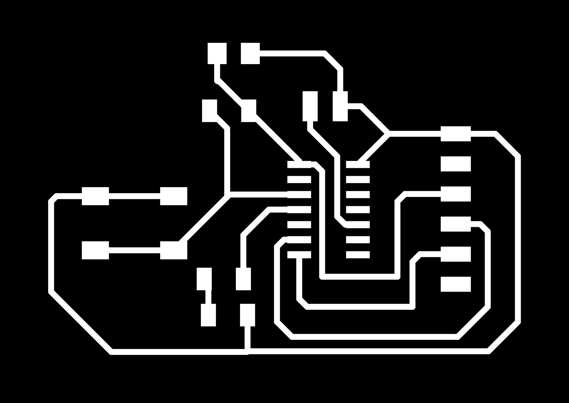
I opened KiCad and created a new project. Using the FAB library that we added during the class, I redrew the hello-world board example with an ATtiny1614, a UPDI connector, a capacitor, and an FTDI connector. I also added an LED, a resistor, and a switch.
To determine which pin to use for the LED and the button, I referred to the following diagram:
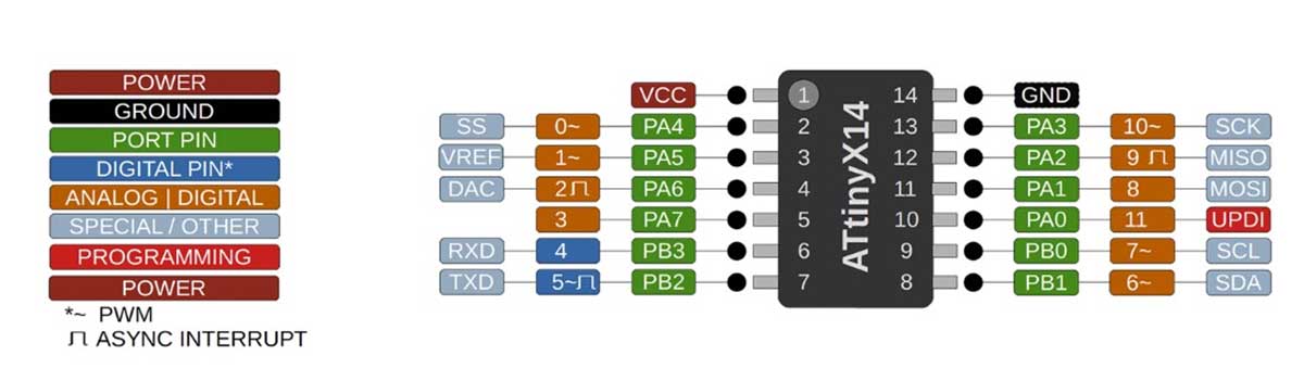
Initially, I used pin number 8, but later I realized that all pins except Ground, VCC, UPDI, and TX/RX were available options.
Initial Attempt
I first created a schematic with the 3216 microcontroller but later corrected it to use the 1614. I kept the file name as 3216, as advised by Oscar, to avoid potential bugs. However, I found that the microcontroller was not utilized effectively in this design.
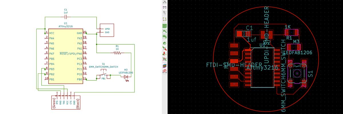
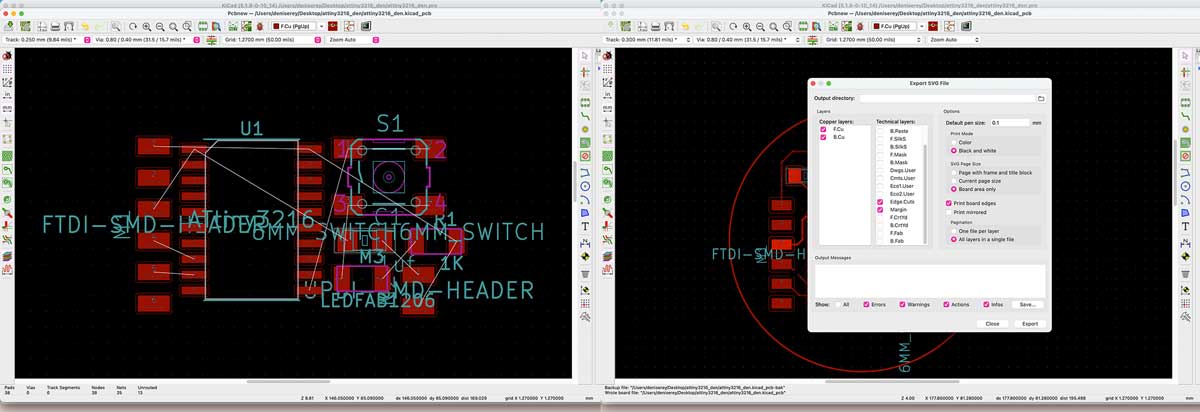
During the lab session, I started exporting the .svg file to open it in Inkscape and convert it to a suitable .png. An instructor pointed out that I should move the LED to another pin to make the design functional. I revised the schematic, adjusted the connections, and added a new resistor.
Options to Check When Exporting to .svg:
- Copper layers: F.CU
- Technical layers: Edge cuts
- Print mode: Black and white
- SVG page size: Board area only
- Print board edges
- Pagination: All layers in a single file
Preparing the .png in Inkscape
After organizing the components, I created the outline and exported the design to .svg. I opened the file in Inkscape and created three layers:
- Background
- Traces
- Interior
- Background Layer: Added a large black rectangle.
- Interior Layer: Moved the outline into this layer and filled the figure with white using the bucket tool.
- Traces Layer: Moved the traces into this layer and turned them white.
I exported the interior and traces separately. For the image definition, I used 1000 dpi.
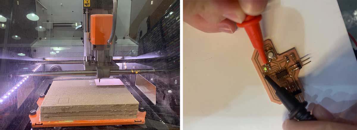
After exporting, I used Mods to mill the PCB.
During the milling process, the instructor noticed that my traces were too thin and the UPDI connector was placed behind the capacitor. I corrected these issues in KiCad, adjusting the trace thickness and repositioning components to make better use of space.
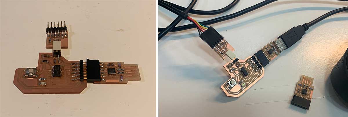
Final Design
For the final board, I selected different pins for the LED and switch to facilitate programming. I also added two 1k resistors, one for the LED and one for the switch.
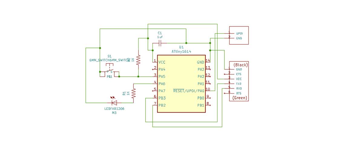
Components Used:
- ATtiny1614
- Capacitor 1µF
- UPDI connection
- FTDI connection
- 2 resistors (1kΩ)
- LED
- Switch
I used the alternative corner for milling as the left-bottom corner was not well leveled. I set the Z-axis to -0.5mm for a proper cut.
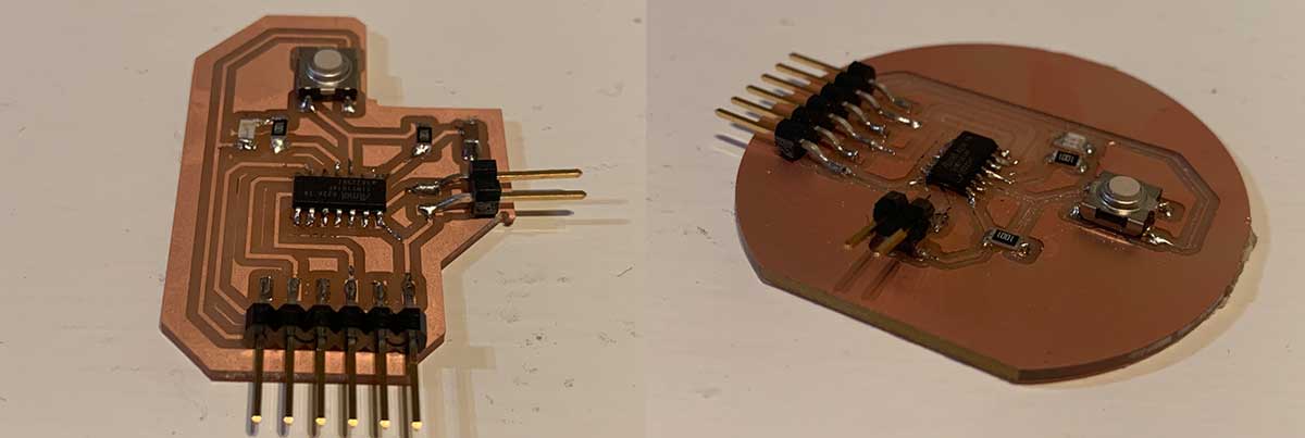
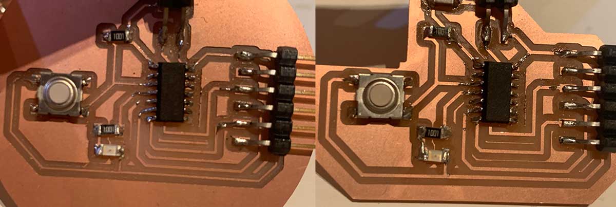
I tested the boards for shorts and connection issues. The LED worked as expected!
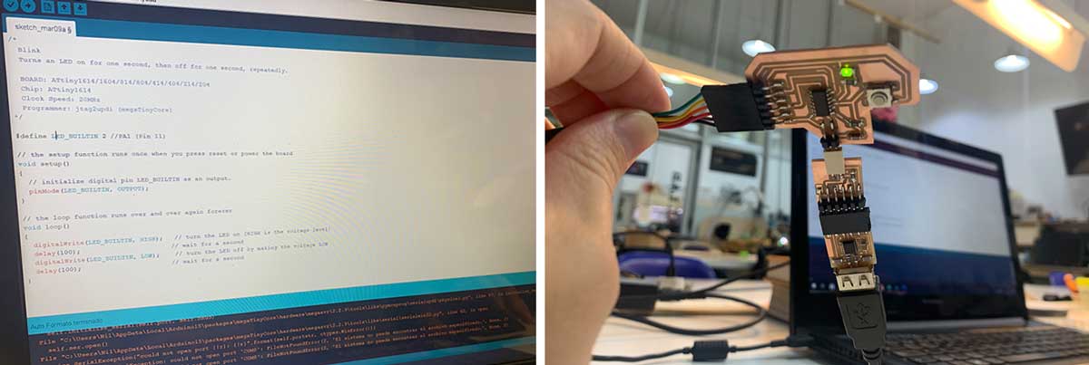
To program the board, I used the FTDI and UPDI connections from week 4 and followed the instructions on this page.
I used Arduino IDE to install megaTinyCore, selected the ATtiny1614 microcontroller, and configured the proper port. I encountered issues on my Mac, which seemed related to the USB connector type.
/*
Blink
Turns an LED on for one second, then off for one second, repeatedly.

BOARD: ATtiny1614/1604/814/804/414/404/214/204
Chip: ATtiny1614
Programmer: jtag2updi (megaTinyCore)
*/

#define LED_BUILTIN 2 //PA6 (Pin 2)

// the setup function runs once when you press reset or power the board
void setup()
{
    // initialize digital pin LED_BUILTIN as an output.
    pinMode(LED_BUILTIN, OUTPUT);
}

// the loop function runs over and over again forever
void loop()
{
    digitalWrite(LED_BUILTIN, HIGH);   // turn the LED on (HIGH is the voltage level)
    delay(1000);                       // wait for a second
    digitalWrite(LED_BUILTIN, LOW);    // turn the LED off by making the voltage LOW
    delay(1000);                       // wait for a second
}
Files
Find all the files here:
Design Rule Check
To properly use KiCad, I followed the beginner guide to KiCad. I also consulted this tutorial on running the Design Rule Check. Initially, I used the default settings for trace width and spacing but found them too thin. I adjusted the settings as follows:
- Min Track Width: Changed from 0.2mm to 0.3mm
- Min Via Size: Changed from 0.4mm to 0.8mm
The Design Rule Check button displays a modal where these parameters can be defined. Errors are indicated with a white arrow and detailed in the modal.
- Clearance: By Netclass
- Min Track Width: 0.3mm
- Min Via Size: 0.8mm
Testing the Board with the Multimeter
Since I was unable to join the group for Raspberry Pi testing, I fulfilled the assignment by testing my new board with a multimeter. I watched this video on how to use a multimeter to guide me through the process.
I compared the board against my blueprint and checked the schematic for correct polarities. Before connecting the board to power, I verified the following:
- Checked for shorts between VCC and GND
- Ensured the microcontroller was soldered in the correct position
Measurements taken included:
- Voltage
- Resistance: To verify resistor values
- Continuity: To test for open or shorted conductors, switch operation, and clear circuit paths