fabstep-i2c
Introduction
This project is inspired by Jake’s fab-step, which is itself a simplified version of uc-bus: a distributed stepper motor controller, each equipped with its own MCU and listening on a common bus (RS485).
With fab-step, this idea was transposed to a millable, single-layer PCB with minimal requirements, so that (fab)labs can easily prototype their own.
This project is a variant that aims at replacing the RS485 with an (amplified) I2C, with addresses being assigned based on topology only.
Problem statement
If this project is successful, we should have a network comprising several stepper motor controllers, meeting the following criteria:
- All nodes are identical, including their firmware: unlike with uc-bus, they are not pre-programmed to listen to a specific channel. Instead, their address (and/or channel) is resolved on the fly.
- Each node has both an input and an output connector. Those cables contain common data and power lines, but also brings an auxiliary daisy-chained line that lets nodes talk to their neighbor, only for resolving topology.
- Node addresses are incremental, starting with the first on the chain (this node has no cable on its input connector).
- The only node that has a USB connection becomes the main controller, and will send messages on the common data line. The data packets from USB have a destination address, and only that node listens to the message content.
- Broadcasts are allowed for e.g. synchronization between all nodes.
In summary, we want a hybrid bus that comprises a multi-drop data line and a daisy-chain auxiliary line for address resolving.
Proposed solution
The hybrid bus would look like this:
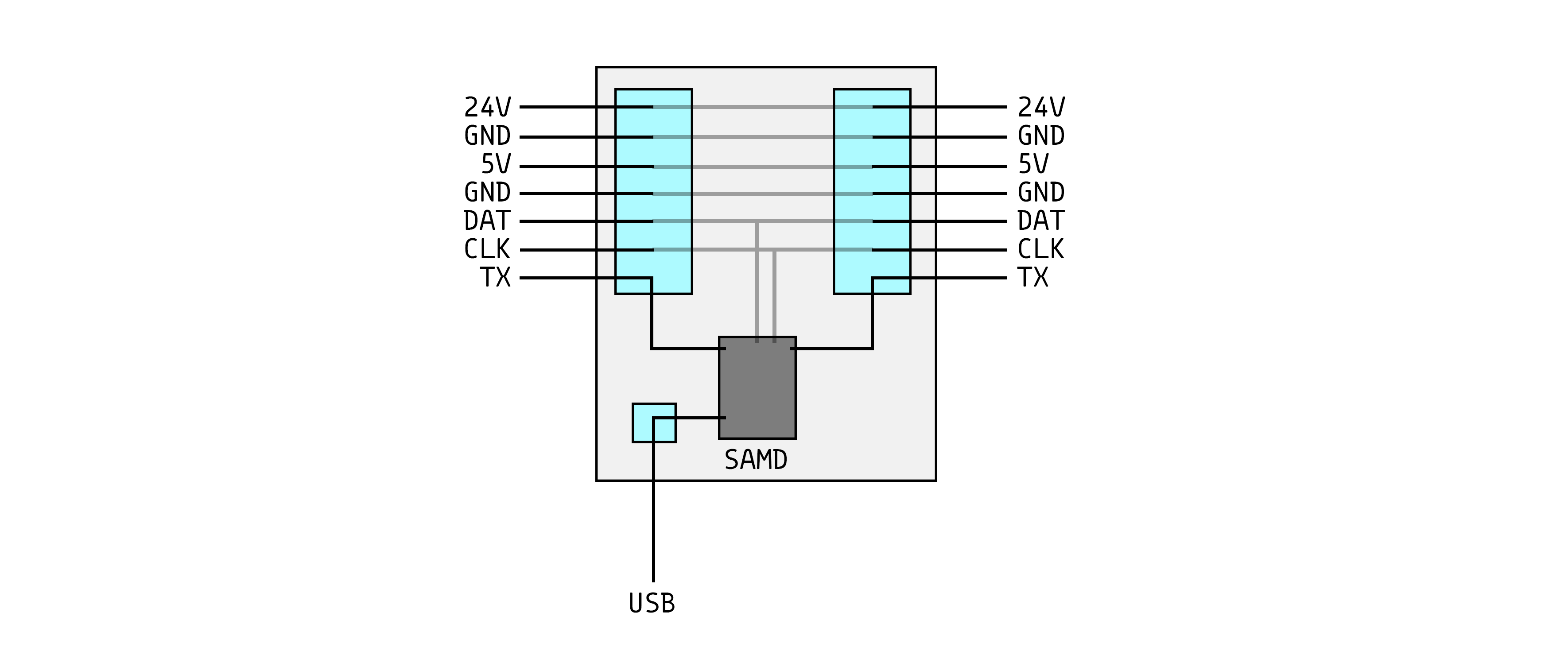
I propose to use I2C for communication, as it only uses 2 wires and can handle addressing. The daisy-chained auxiliary line can be as simple as a serial line going to the next node. The benefit of this is that only 1 hardware serial is used on the MCU, but it can only listen to the previous node. Since there is no information flowing backwards, the last node has no idea it’s at the end of the line unless it can sense that the connector is missing. I propose to handle this with a dedicated pin on the connector.
Having two connectors on the board lets users change the topology with limited effort. For instance, an additional node can be added after the last node by just connecting a point-to-point cable.
My main concern is the current flowing through the cable and the boards. I’m afraid the sum of the currents needed for all following nodes flowing through the first node might be too much. In that case, a star topology for only the power lines could be useful.
One last important point is proper termination of the I2C line. I2C is open-drain, so it requires pull-up resistors somewhere on the line. I think it’s best to have a pull-up at each end of the line (first and last node), but not on every node in-between. This requires pull-up resistors that can be enabled on-the-fly, based on the detected topology.
Update 2021/02/18
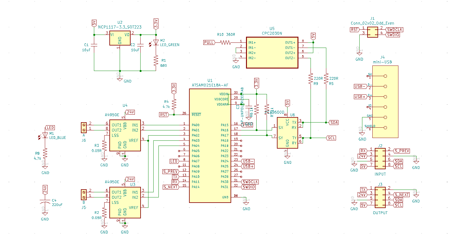
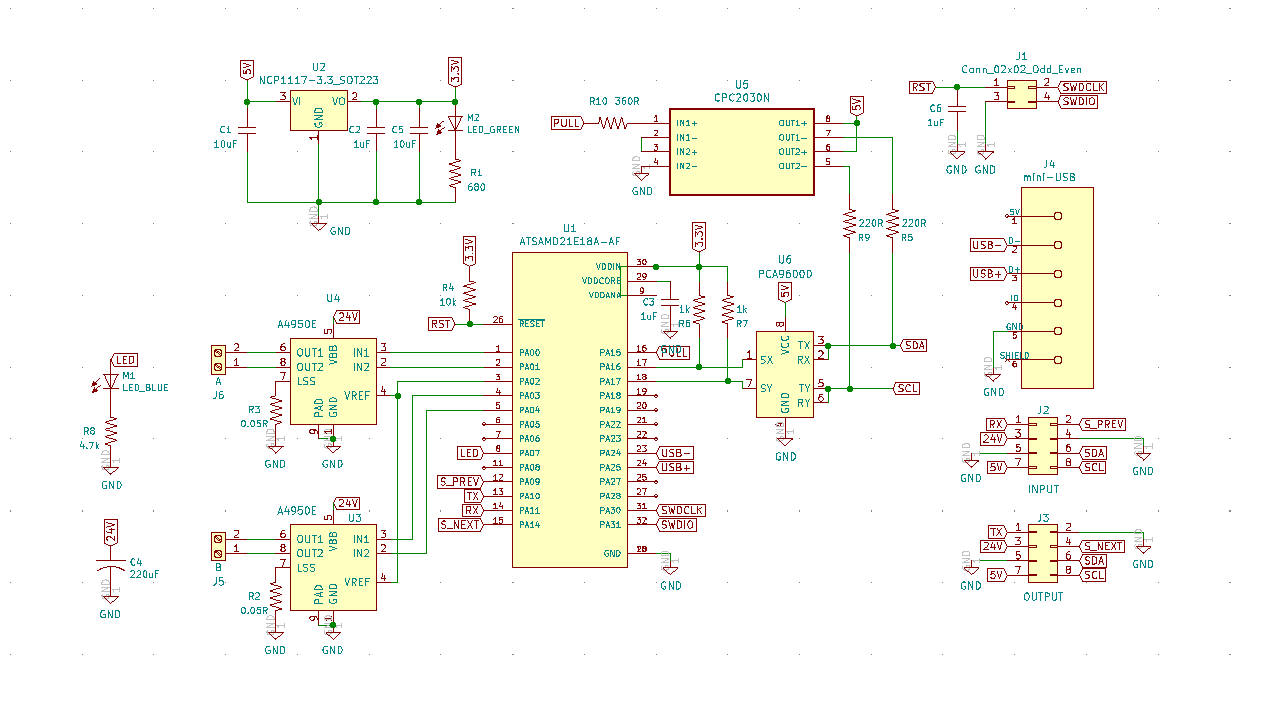
Schematic
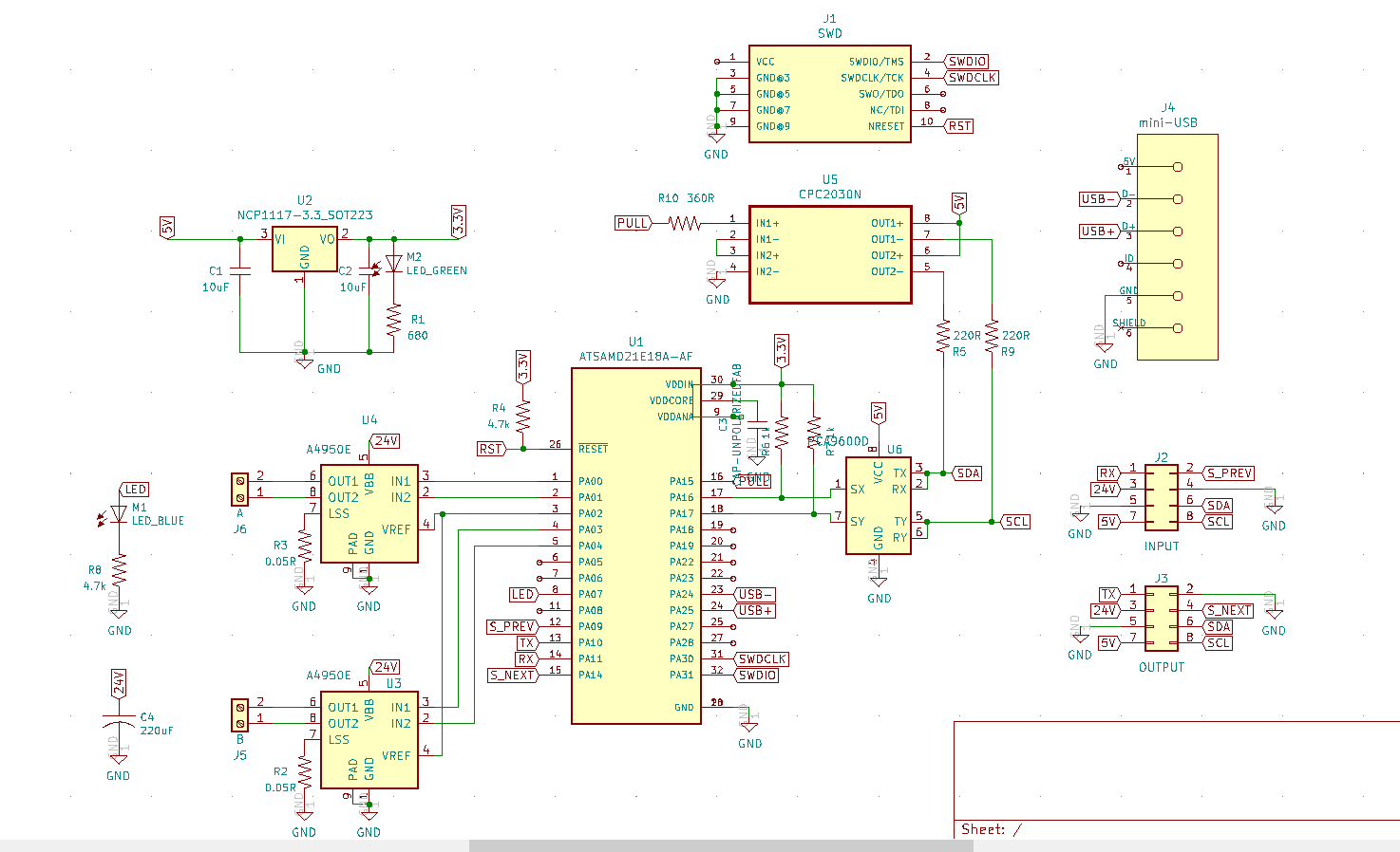
The schematic is rather straightforward. Each node has a mini-USB connector going to the SAMD21, which controls two H-bridge modules and an I2C driver, on which pull-up resistors can be enabled using a solid-state relay.
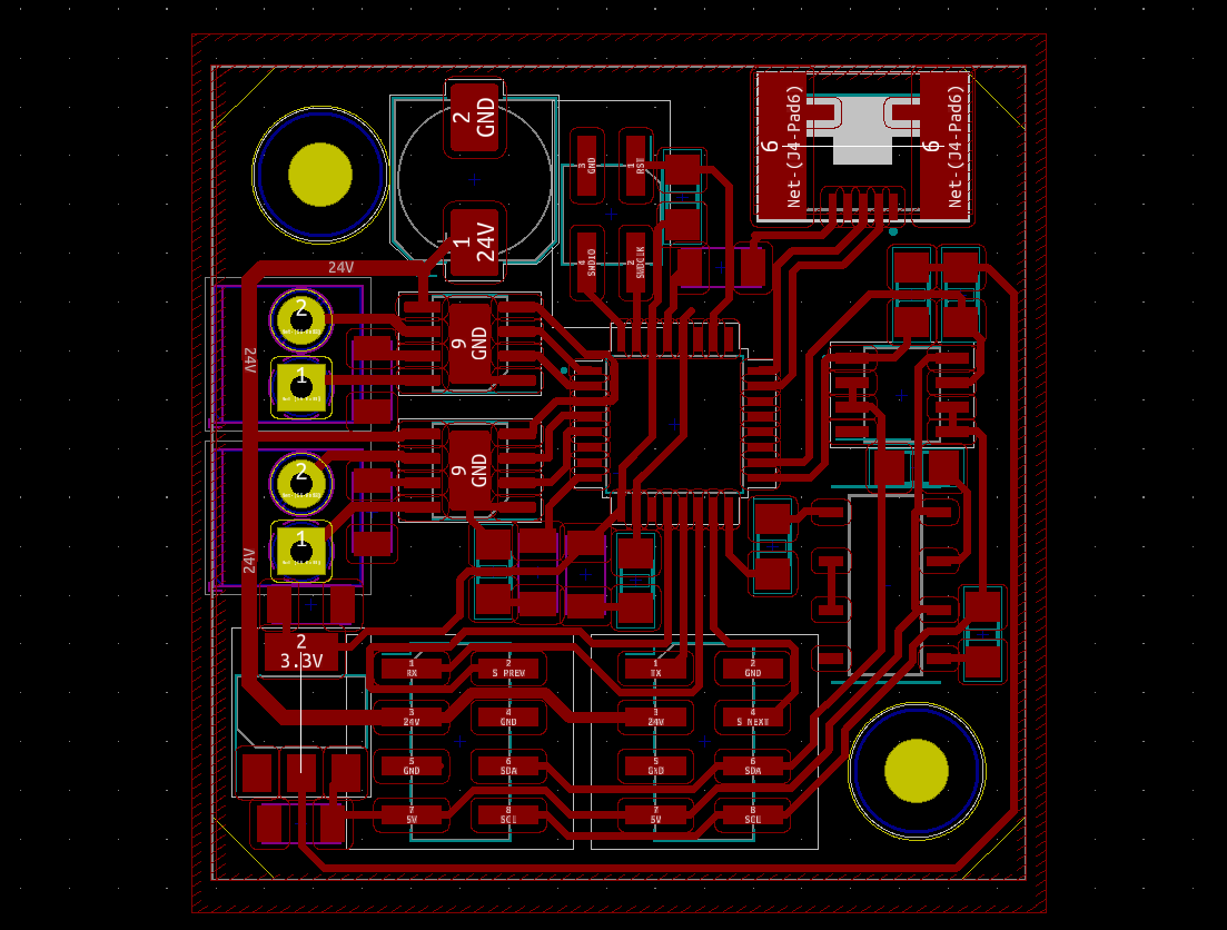
The input/output connectors for the bus comprise 4x2 pins:
- GND
- 5V
- 24V
- SDA
- SCL
- RX (TX of previous node)
- TX
- sense_previous (pulled to GND if input connector goes to a node)
- sense_next (pulled to GND if output connector goes to a node)
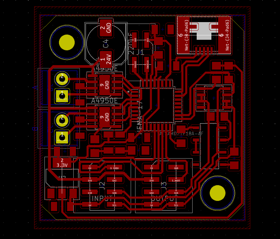
Board
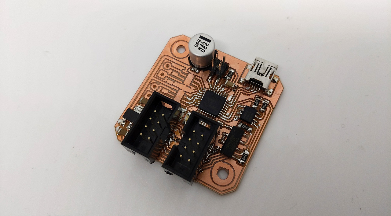
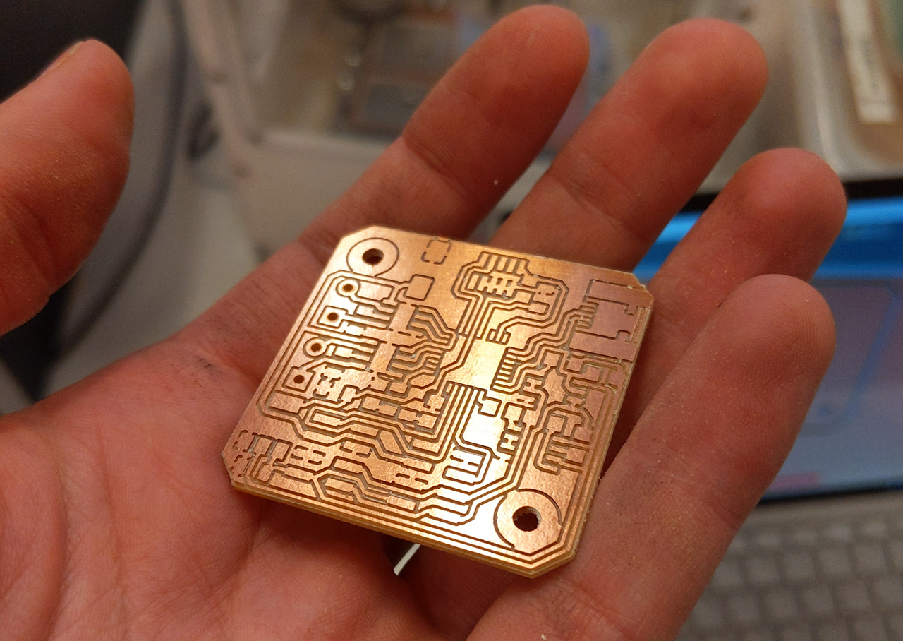
As with fab-step, the board is designed to be millable with a 1/64” flat-end mill. It has the same form factor as a NEMA17 motor on which it should be mounted, including two holes for mounting.
The input/output connectors are visible at the bottom of the board. On the right side you can spot the I2C driver and a 2-channel solid state relay for the pull-up resistors.
Unfortunately, at the moment I could not find a SOIC-8 solid-state relay. I hoped to use a CPC2030N but it turned out to be 2.54mm pitch instead of 1.27mm. I need to replace it or find enough room for the CPC2030N (not possible?).
I milled the board with a 1/64” flat end mill just for testing and it came out just fine.
Update 2021/03/01
I removed the 10-pin JTAG connector and replaced it with 2x2 pins for two reasons:
- There was almost no room to actually connect to that (capacitor on the left)
- This gives us 2 free pins (SWDIO and SWCLK) that can be used to connect endstops or such
Thanks to this, I could finally fit the CPC2030N solid state relay. I also replaced the 5mm screw terminals with 3.5mm for saving some space.
The schematic is mostly identical:
Next step is milling and testing one prototype. Let’s proceed in this order:
- Solder only USB+SAMD+JTAG pins and program it
- Add I2C side and test out simple I2C commands
- Add H-bridge and test motor rotation with either 12V or 24V
- Test current regulation
If all is OK, I can produce another board and start writing the protocol.
Update 2021/03/04
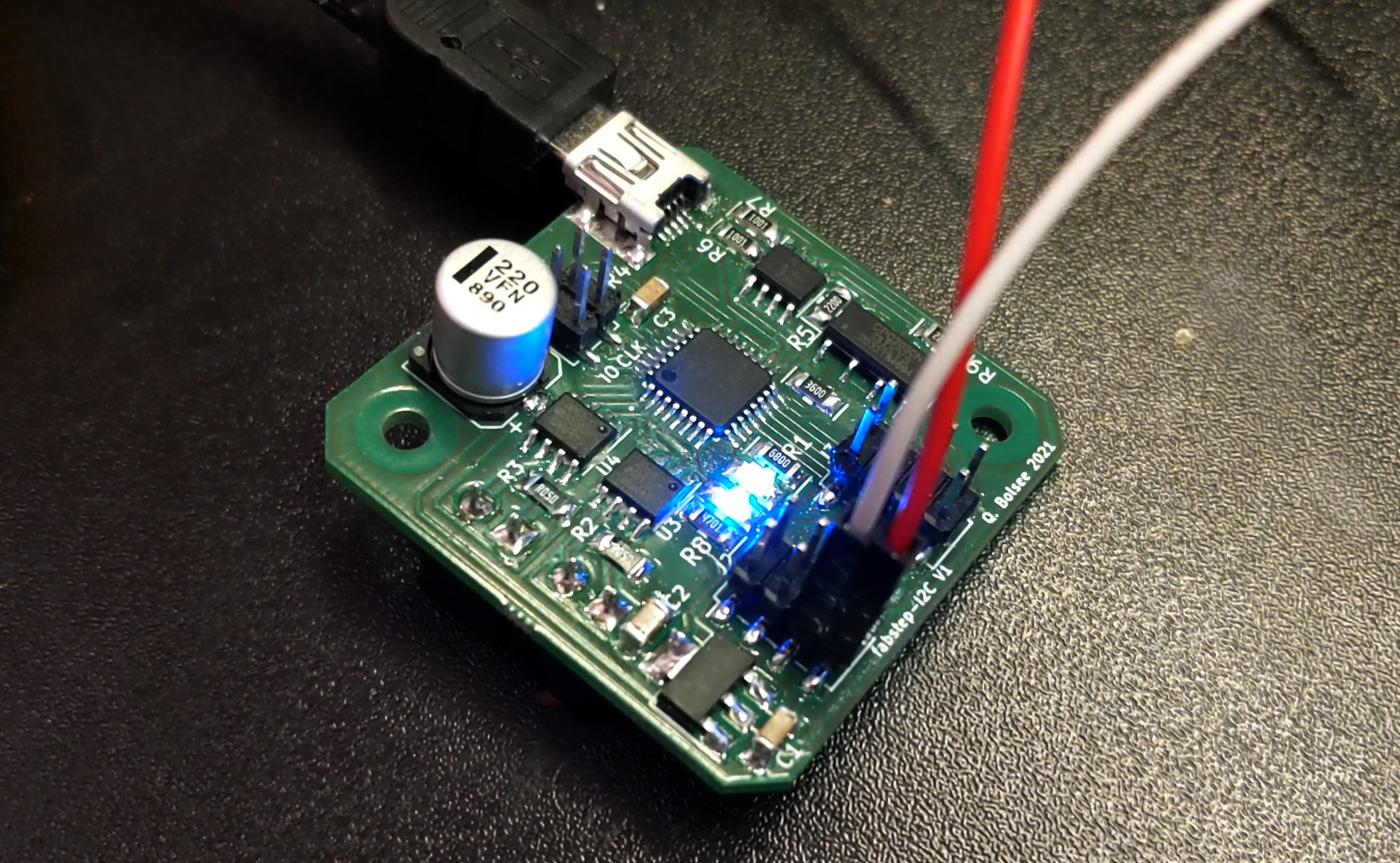
I finally found time to mill it and solder most components. For now I leave the H-bridge missing so I can focus on the I2C communication.
This was a bit tricky to solder, but only because of the shrouded connectors. The shrouds are too large and prevent good positioning of the iron tip.
Update 2021/03/20
There was a short circuit and I lost my first prototype, so I decided to manufacture some industrial prototype instead. No that’s not cheating! The board is still single-sided and millable with a 1/64” flat end mill. The manufactured board is identical but now includes an optional solder and silk mask (added in this repository).
I successfully flashed the SAM BA bootloader and tested the I2C part with no trouble.
Update 2021/03/22
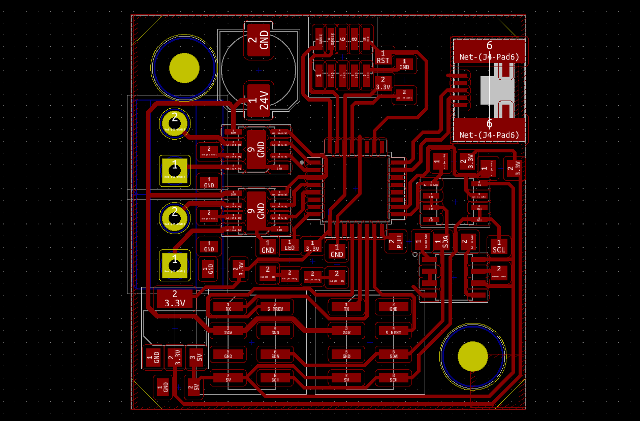
When testing the A4950 with an actual NEMA 17 stepper attached, I noticed some serious interference with the SAMD, causing a systematic reset. I traced it down to a brown-out on the internally regulated 1.2V, most likely caused by a dip in the 3.3V coming to the SAMD. Moreover, the RESET pin was extremely sensitive, triggering a reset for seemingly no reason whenever I touched it with a (high impedance) probe. I added two components to solve these issues:
- A 10uF capacitor between 3.3V and GND, as close as possible to the microcontroller. I only had one close to the regulator, and the distance was enough to cause interference from the A4950.
- A 1uF capacitor between RESET and GND to stop spurious reset triggers.
I had to solder these in an unorthodox way for now, but I already prepared a new board and schematic:
Here is a test of the motor spinning:
License
This project is provided under the MIT License.