Individual assignment
First attempt
Although Ricardo suggested I could design another board, this time with a Xiao, I didn’t really understand that I’d be doing this a couple more times, so I thought I could save some time and go with the board I already designed the previous week. Little did I know 😅
This was the plan:
- extract gerber and other files from kicad
- import into Easytrace5000
- export nc files from Easytrace5000
- check files with ncviewer
- feed it into candle
- mill board
- solder
- test
For brevity, I’ll skip the intermediate steps getting from Kicad to the end product, as I missed those and will document again in my 2nd attempt.
However I’ll document the failed attempts and the end result.
There were a lot of attempts like this one, where I was still trying to mill the original design, where the cuts would be too deep, not deep enough, or more surprisingly not deep enough in just some parts of the milling.
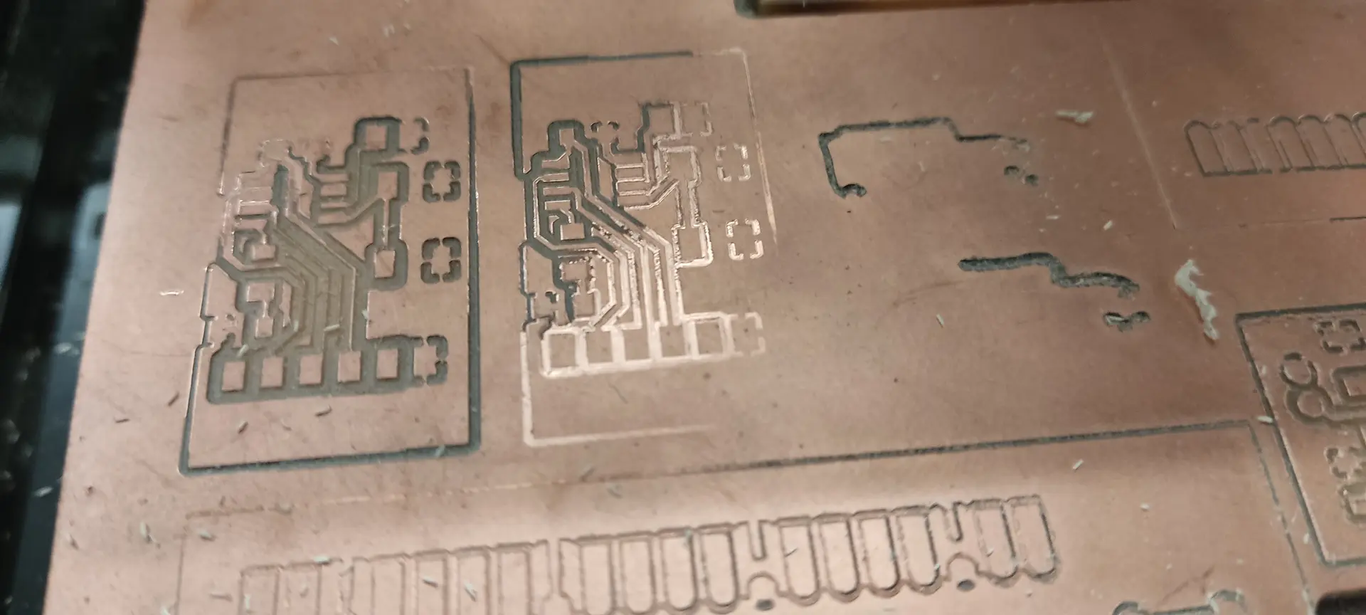
Eventually I realized that, despite doing Z probing, the board would bend under pressure from the end mill cutter, when milling, rendering the Z probing not effective.
I tried pressing down the board while doing Z probing to try to account for the bending:
But that did not really solve the issue.
Eventually using a clamp on the edge of the board and a new end mill cutter solved the issue:
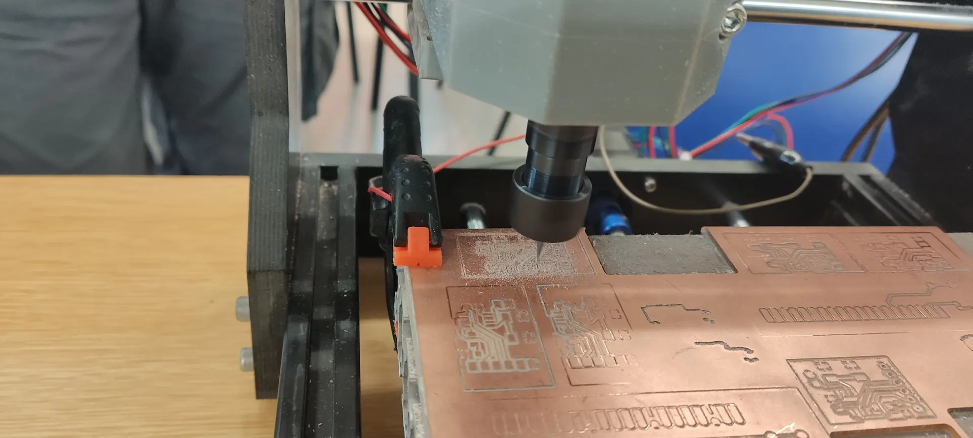
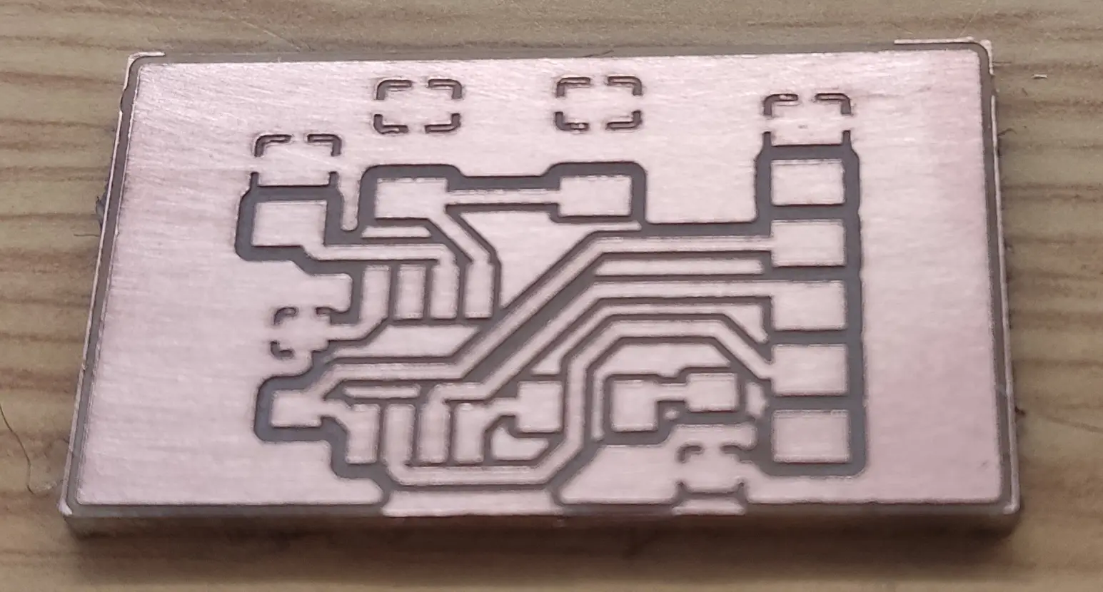
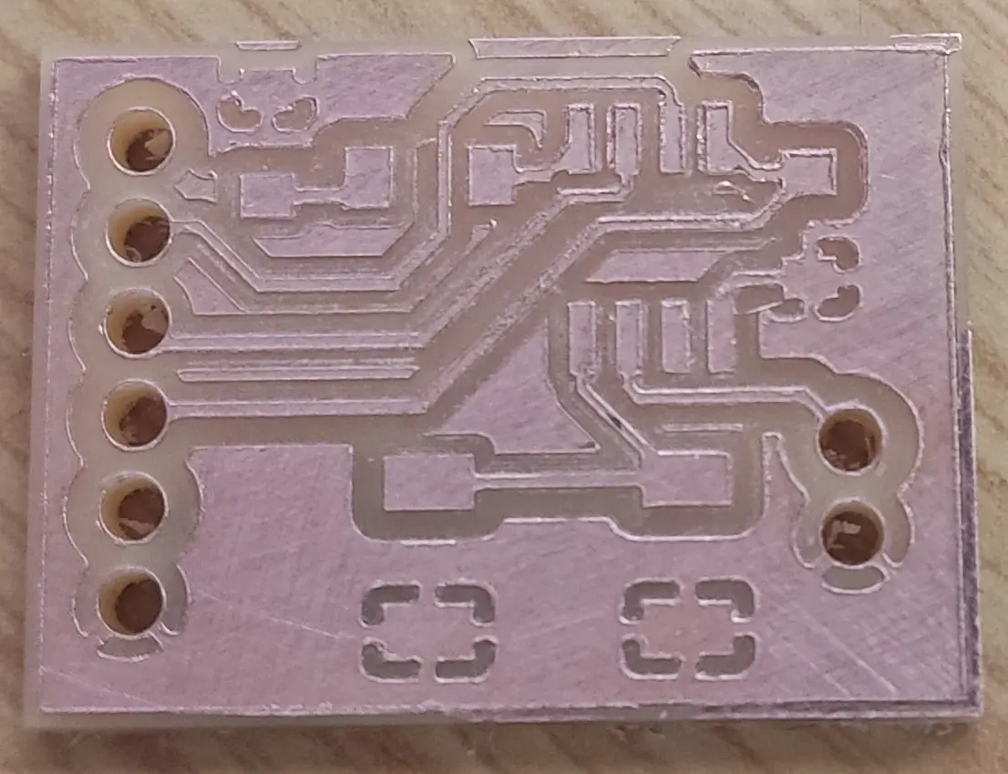
And we got to the final board.
I then tried soldering, but everything is too tiny and I needed a magnifying glass 🔍 😅
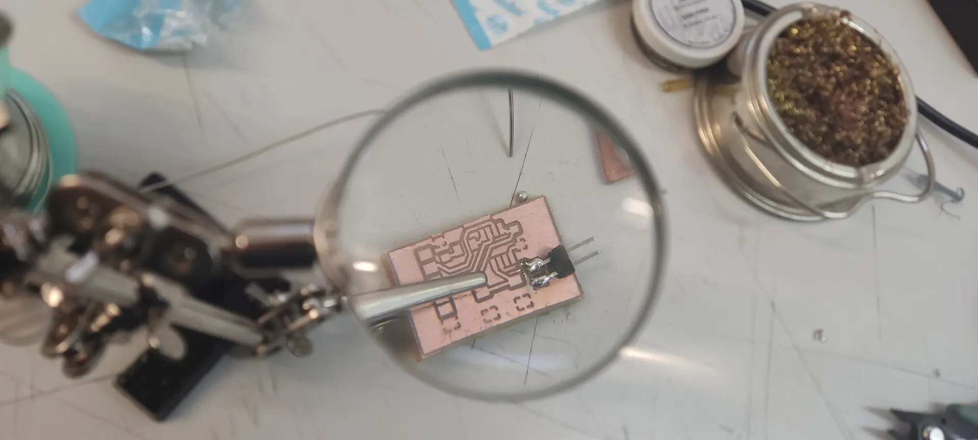
My soldering skills are not that great, and I had some help, and at some point we used reflow soldering:
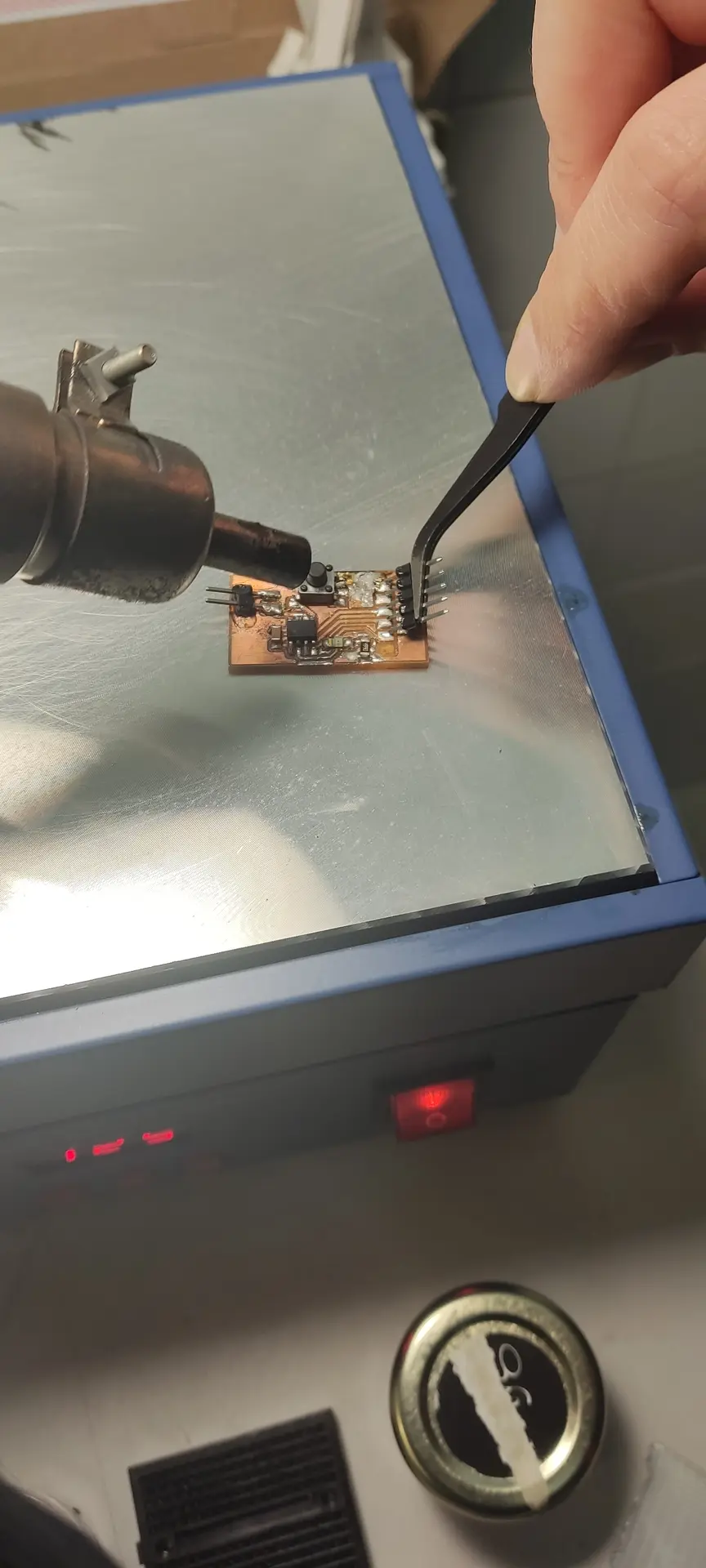
Reflow didn’t quite work for the larger pins, so the best I got this week was this:
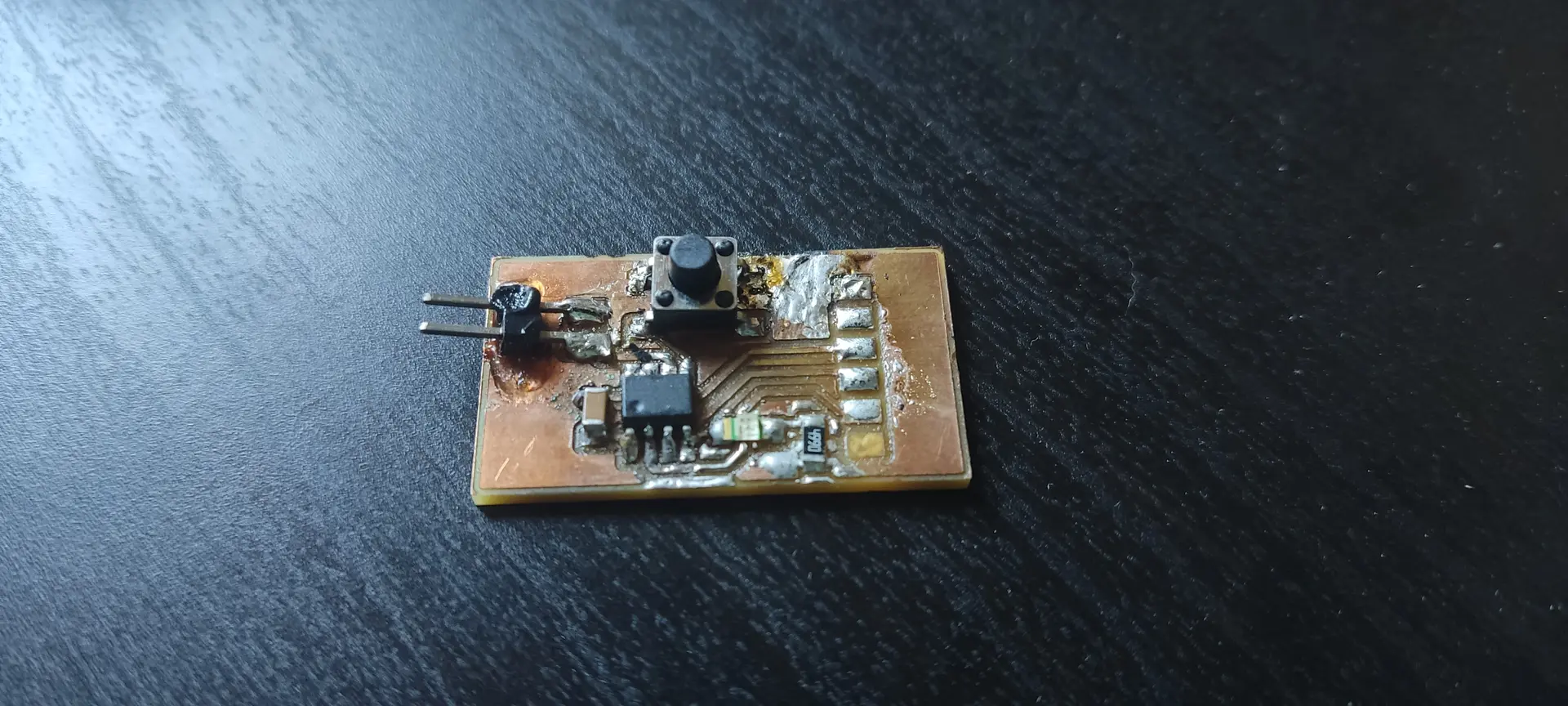
Looking at this big pile of 💩 I’d be surprised if this worked at all 😅
Regarding soldering, I wrote a whole page on it that you can read here
While we were dealing with this board I also let another one milling where we replaced the pins with through-hole ones, but I never actually did anything with it, because another week had started and I got a better understanding of the Xiao’s which I preferred.
Second attempt
After doing the class on networking week, and doing the board for the output week, I had a chance to come back here and finish this assignment.
On week 9 I describe the design of the board, and on this week I focus on its production.
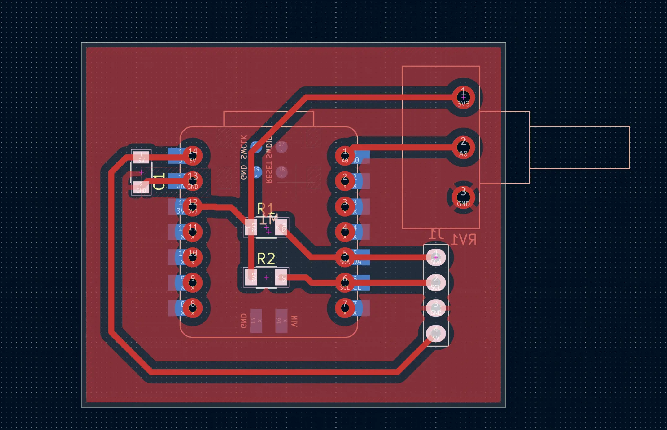
Design of the board
Here’s what the board looks like, as designed in Week 9:
Exporting files from KiCad
It’s now time to produce the board by milling it. I shall use Easytrace5000 for this purpose.
But first we need to export the board designed in KiCad into a few files that Easytrace5000 understands:
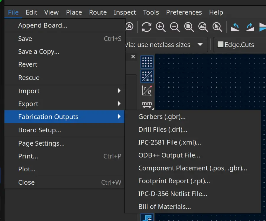
We select Gerbers, and activate the checkbox for “Use Protel filename extensions” and click Plot:
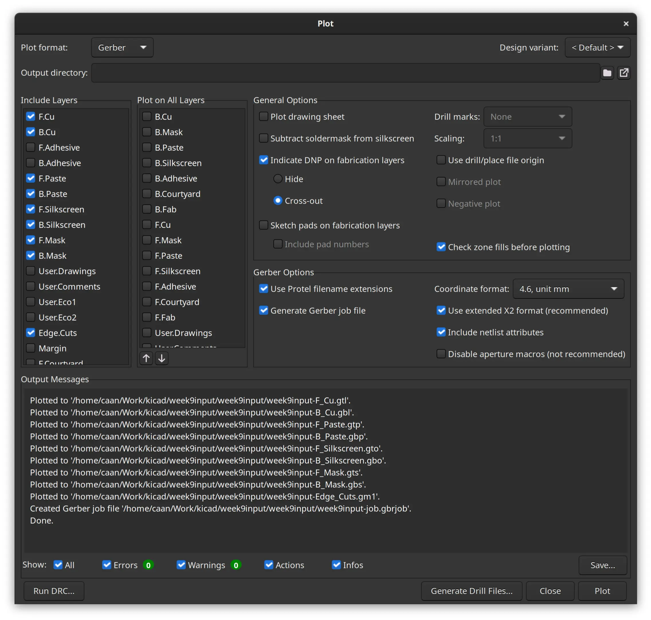
A number of files will be generated. We also select the “Drill files” and click Generate:
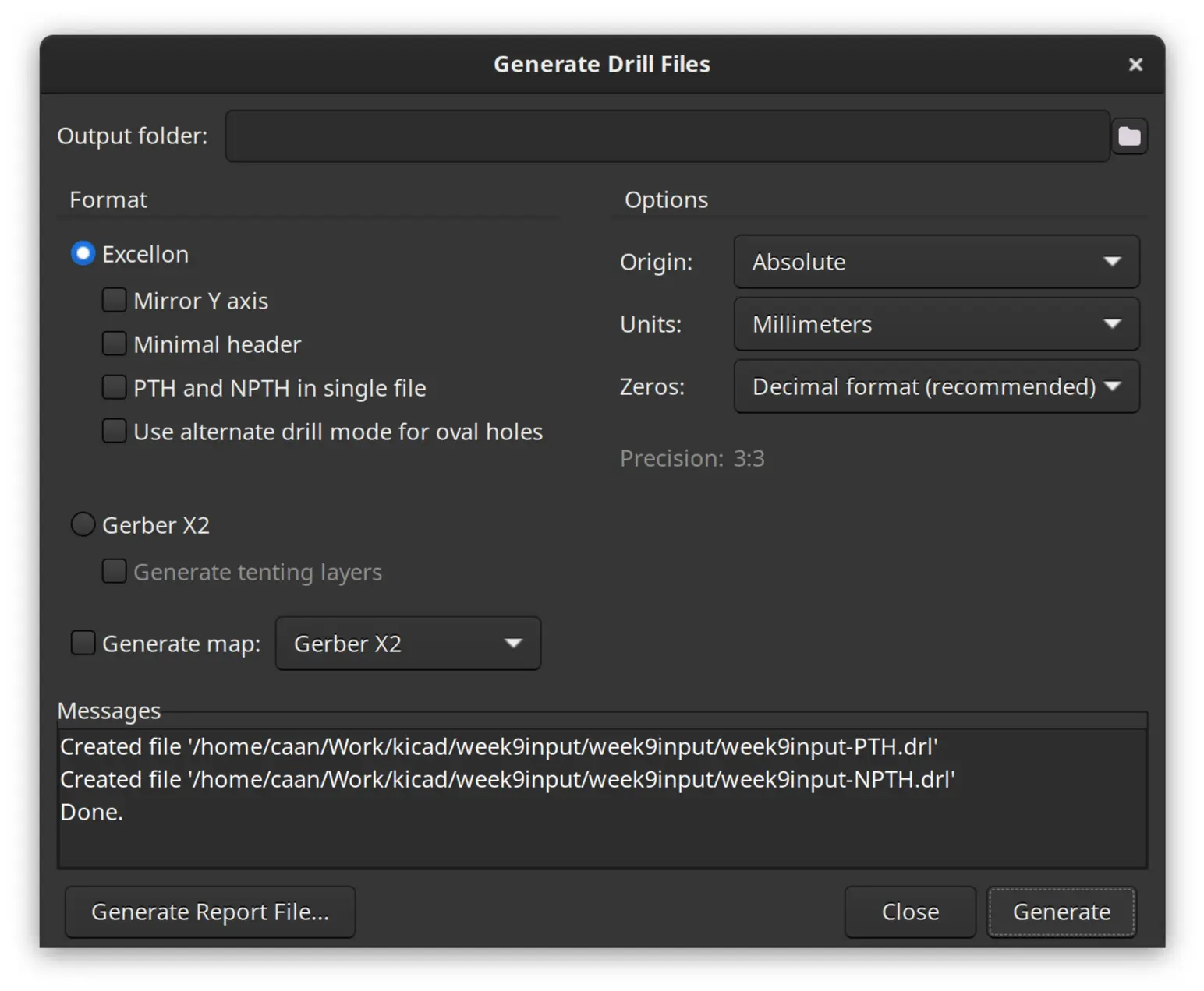
A couple of files are generated.
We are now ready to import into Easytrace5000
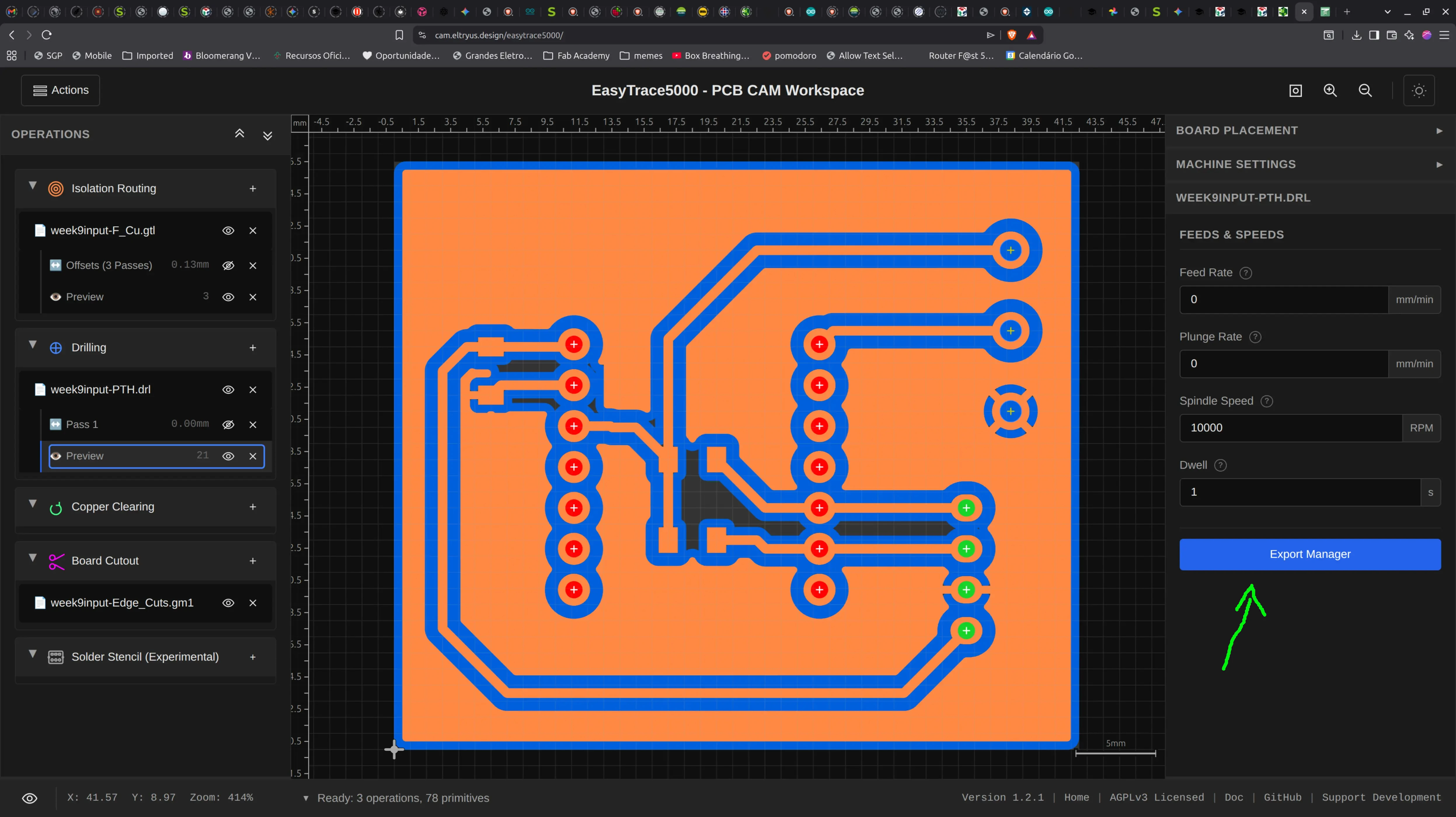
Calculate toolpaths with Easytrace5000
We open Easytrace5000 url in the browser:
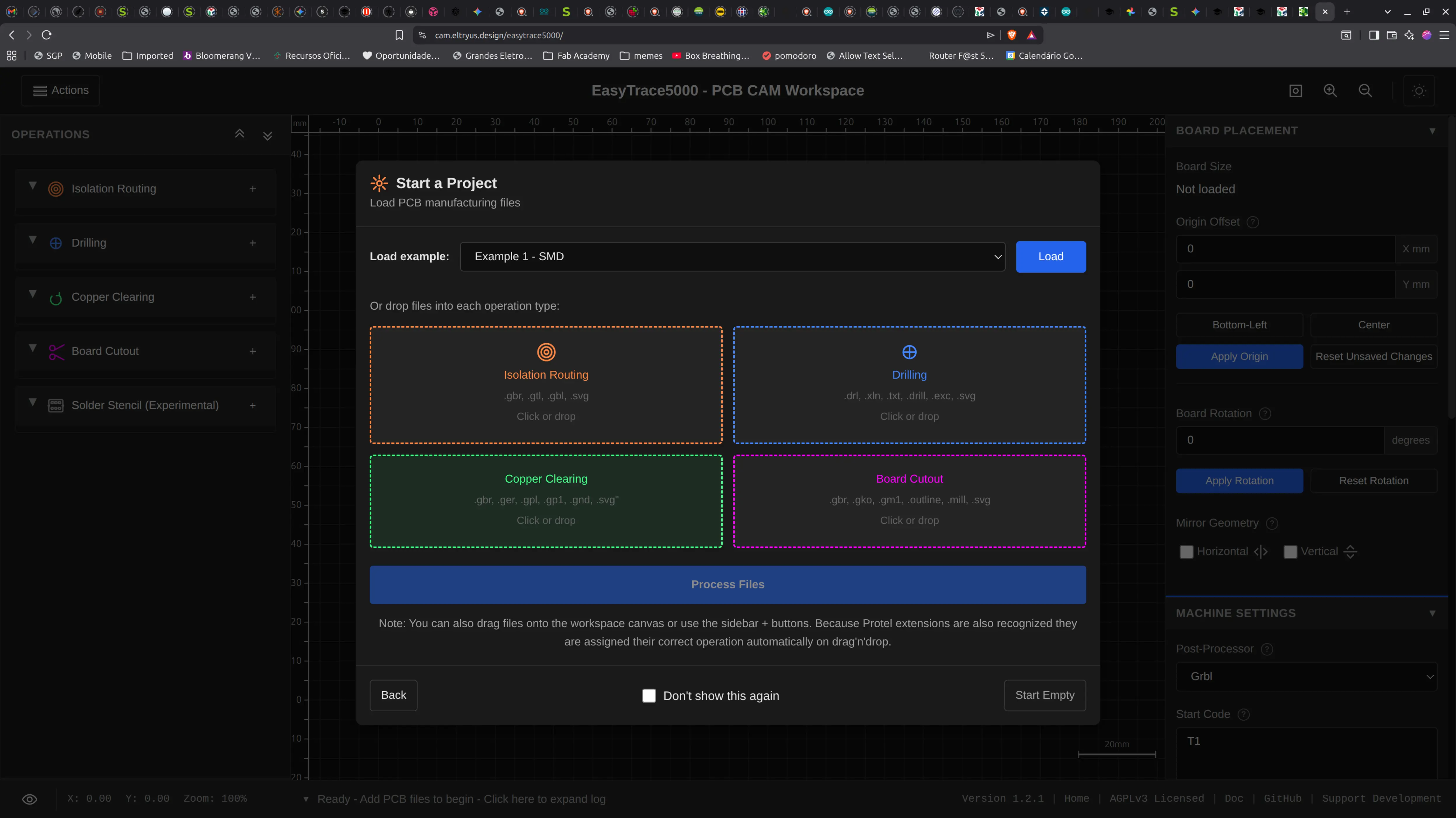
We click in “Isolation Routing” and select the file ending in “F_Cu.gtl”, then click on “Drilling” and select the file ending in “PTH.drl”. Finally we select “Board Cutout” and select the file ending in “Edge_Cuts.gm1” and click “Process files”
It looks like this:
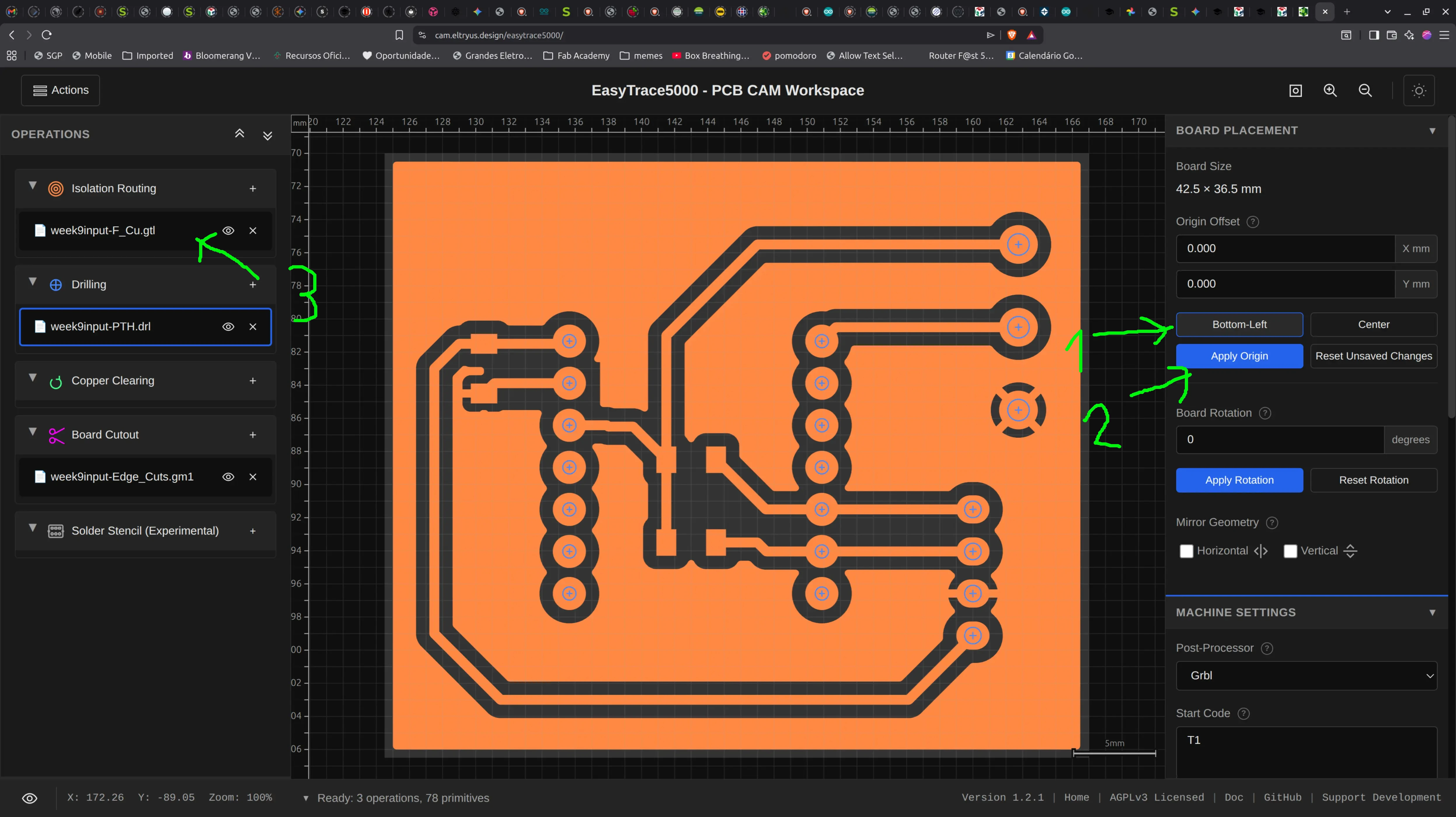
We the click in “Bottom left” and “Apply origin” and keep the remaining parameters as default.
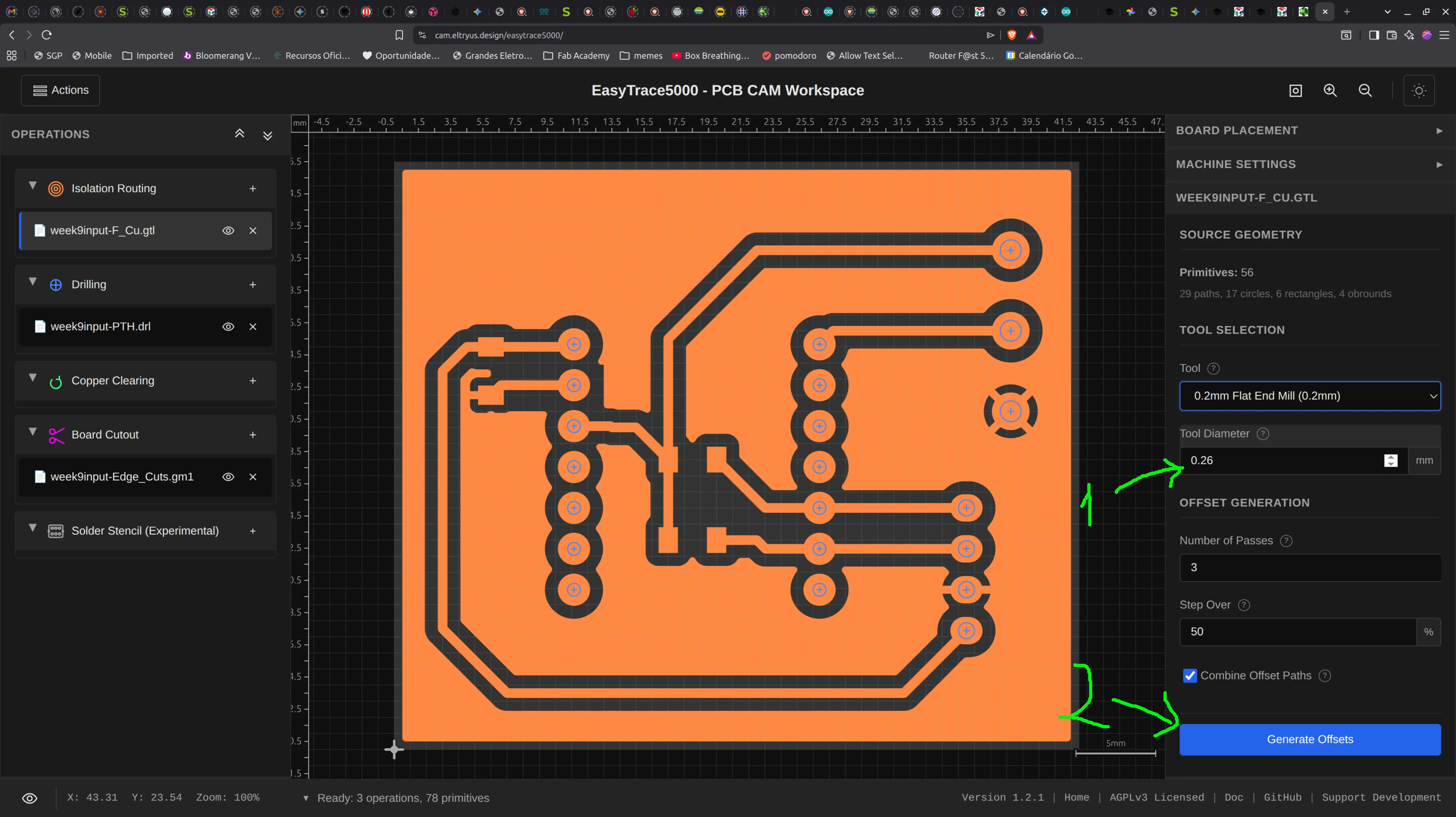
We click on the Gtl file preview on the left, and then a tool selection on the right appears.
I change the “Tool Diameter” to 0.26 mm which is adequate to our V-bit mill.
I leave the remainder settings as default and click “Generate Offsets”:
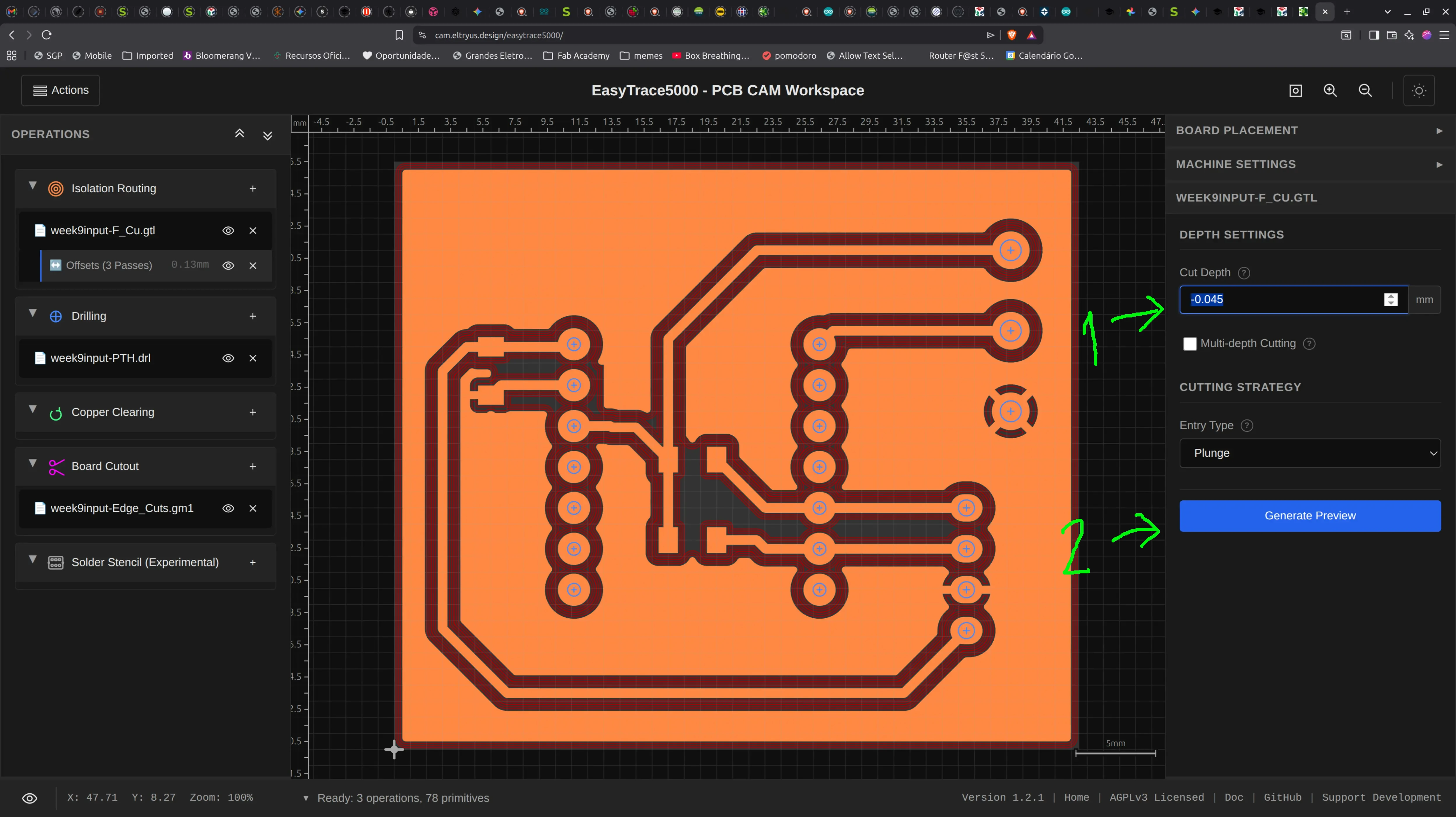
I change the “cut depth” to “-0.045” mm and click “Generate Preview”:
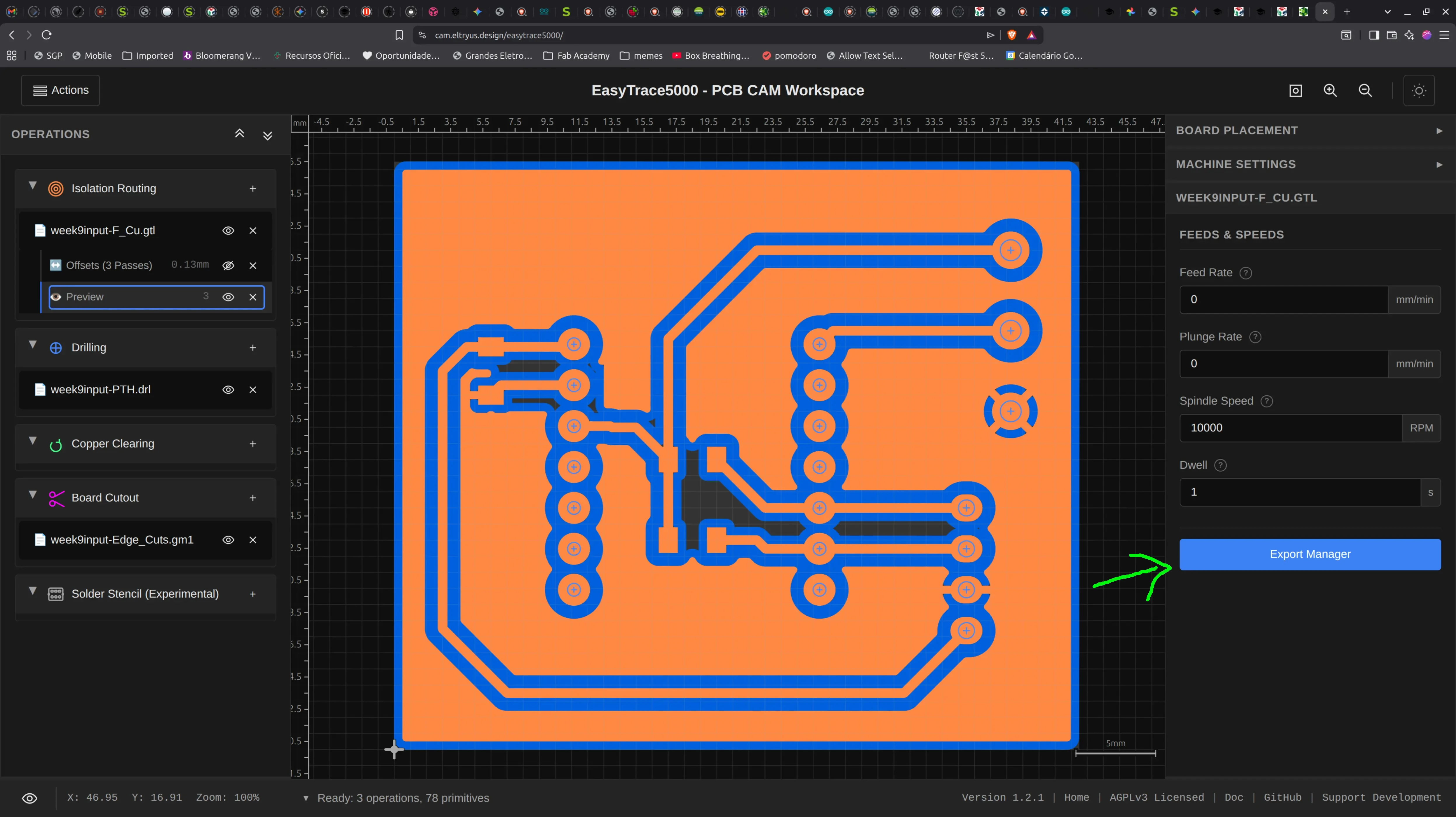
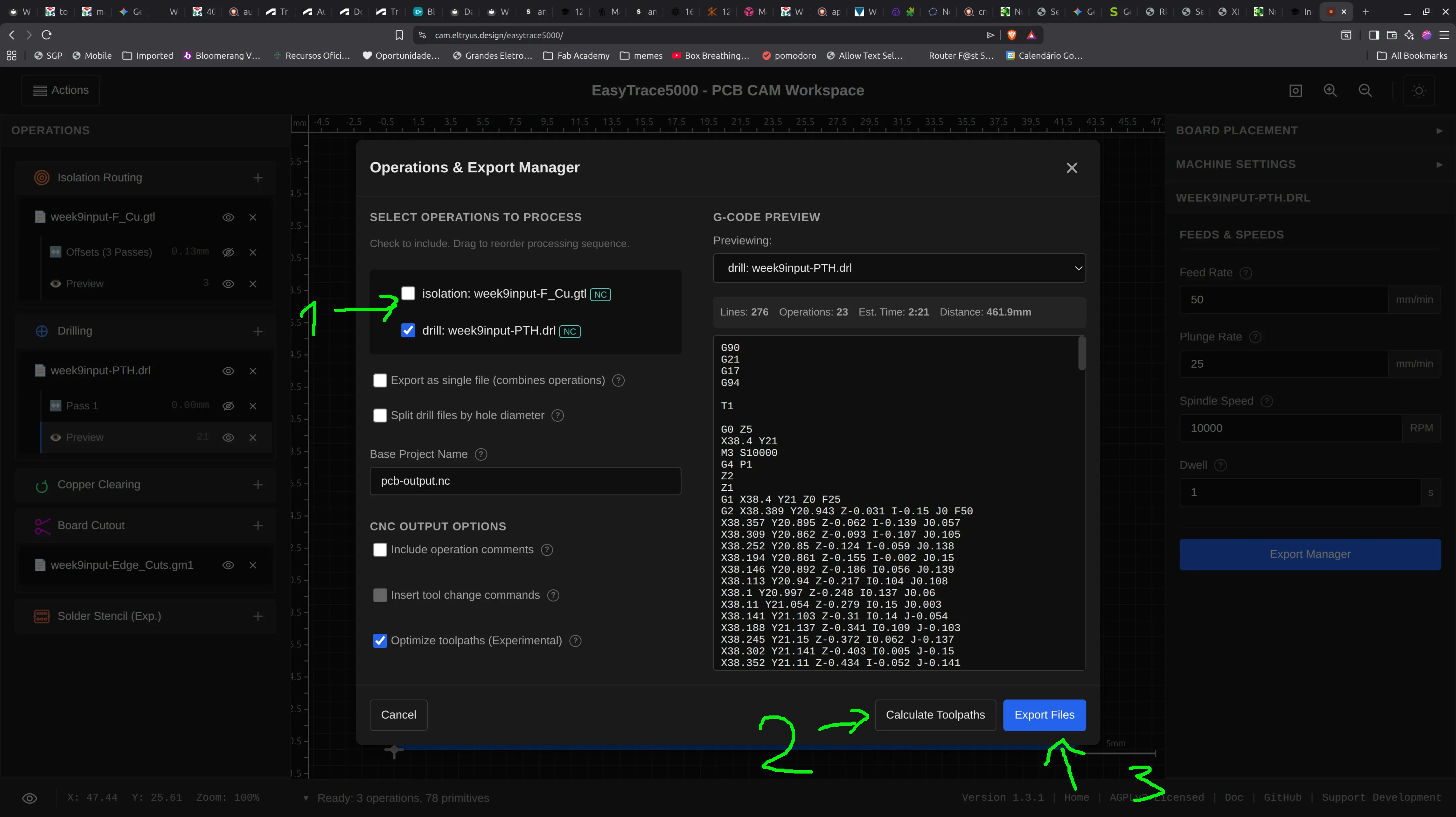
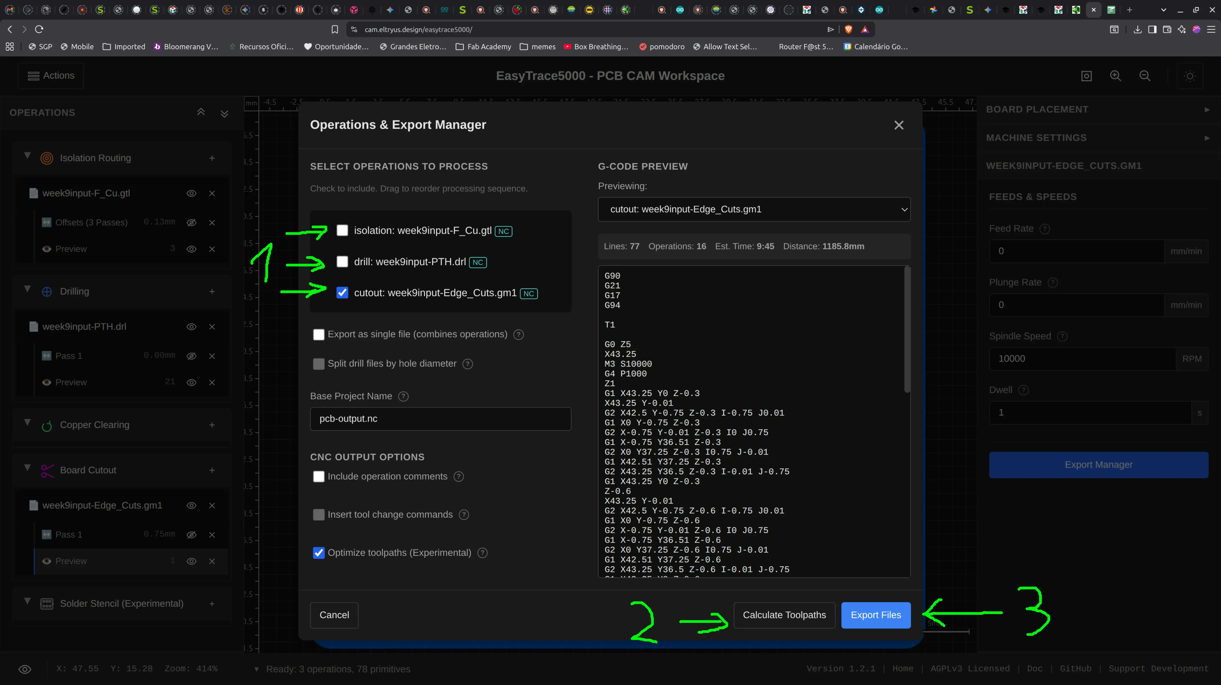
I then click “Export manager”
I then deselect the option “include operation comments”, click “Calculate toolpaths” and then “Export files”
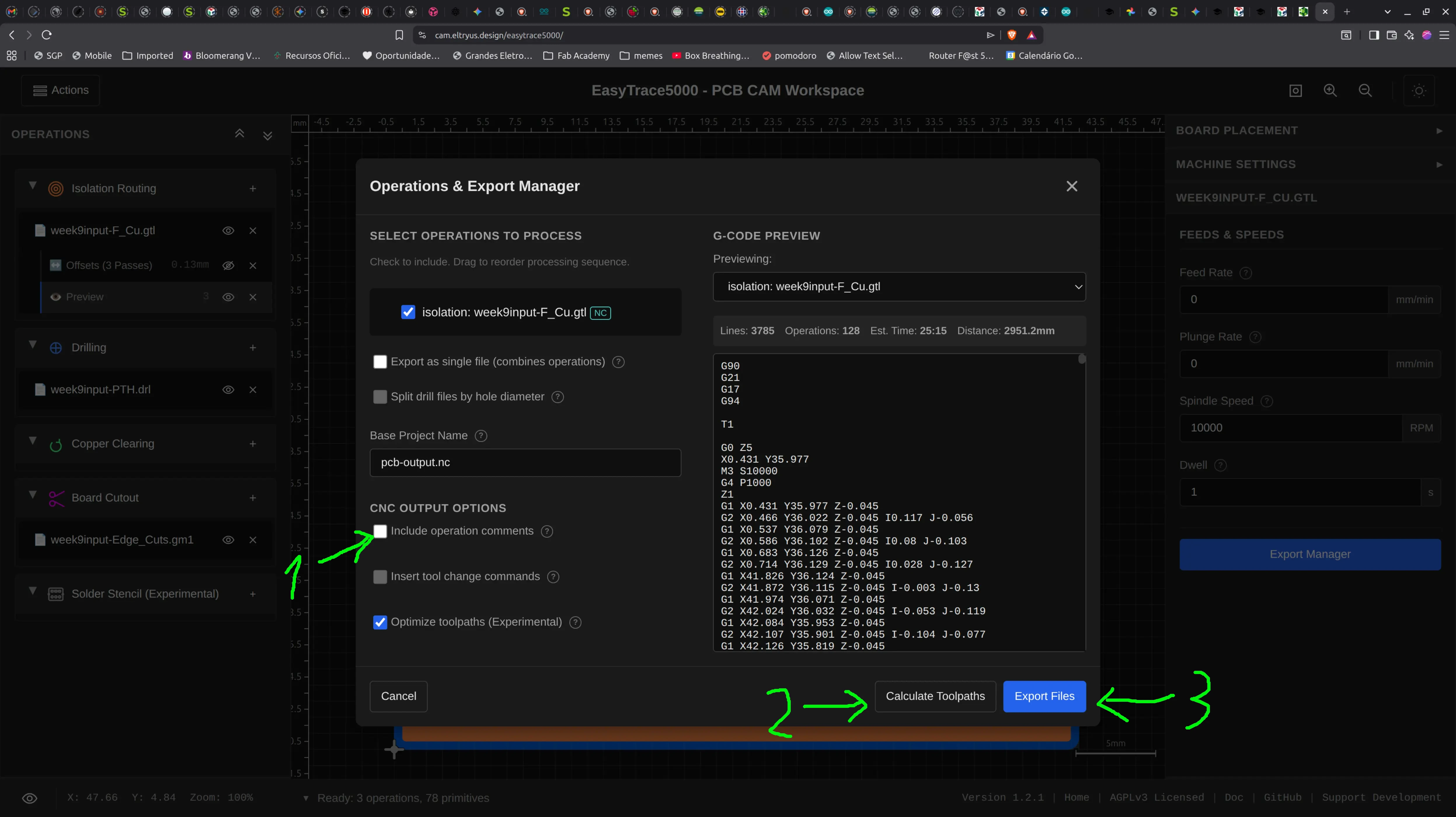
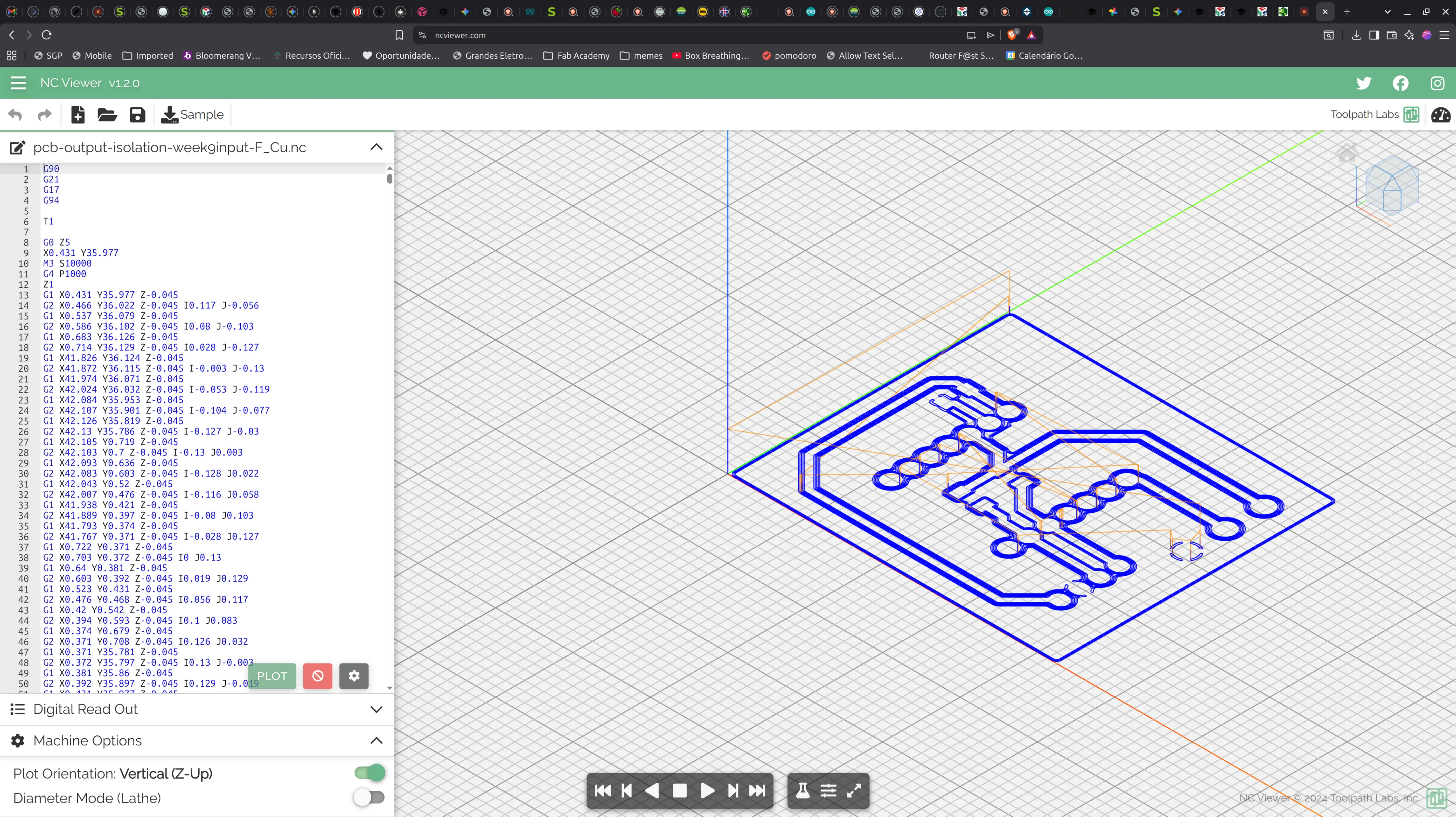
A file called “pcb-output-isolation-week9input-F_Cu.nc” is saved.
We can use Ncviewer to check that everything looks good:
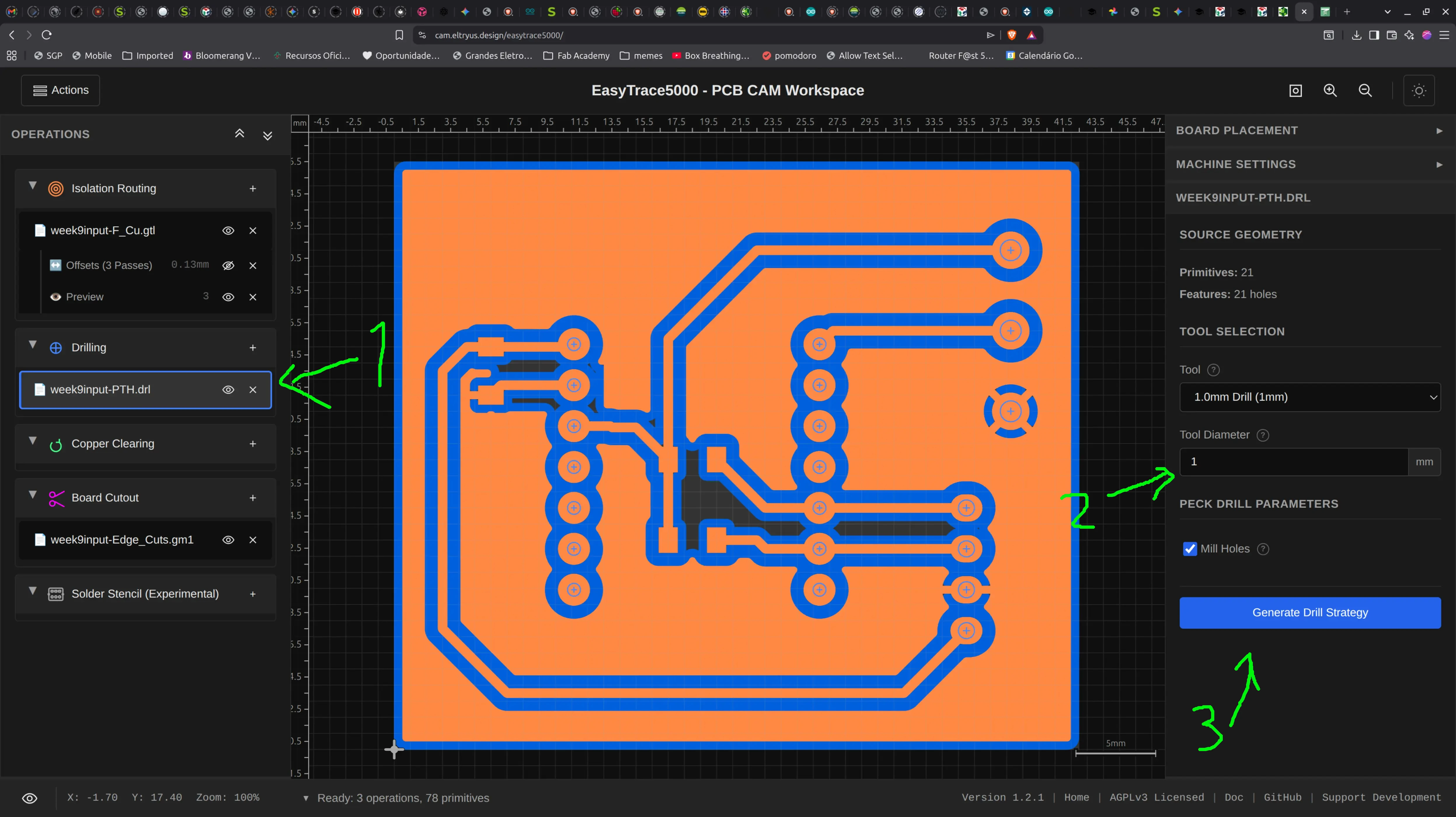
We go back to Easytrace5000 and click the “.drl” file preview, check that the “Tool diameter” is 1 mm because that’s what we’re going to use, and then on “Generate Drill strategy”:
We can accept the tool’s defaults and just click on “Generate Preview”
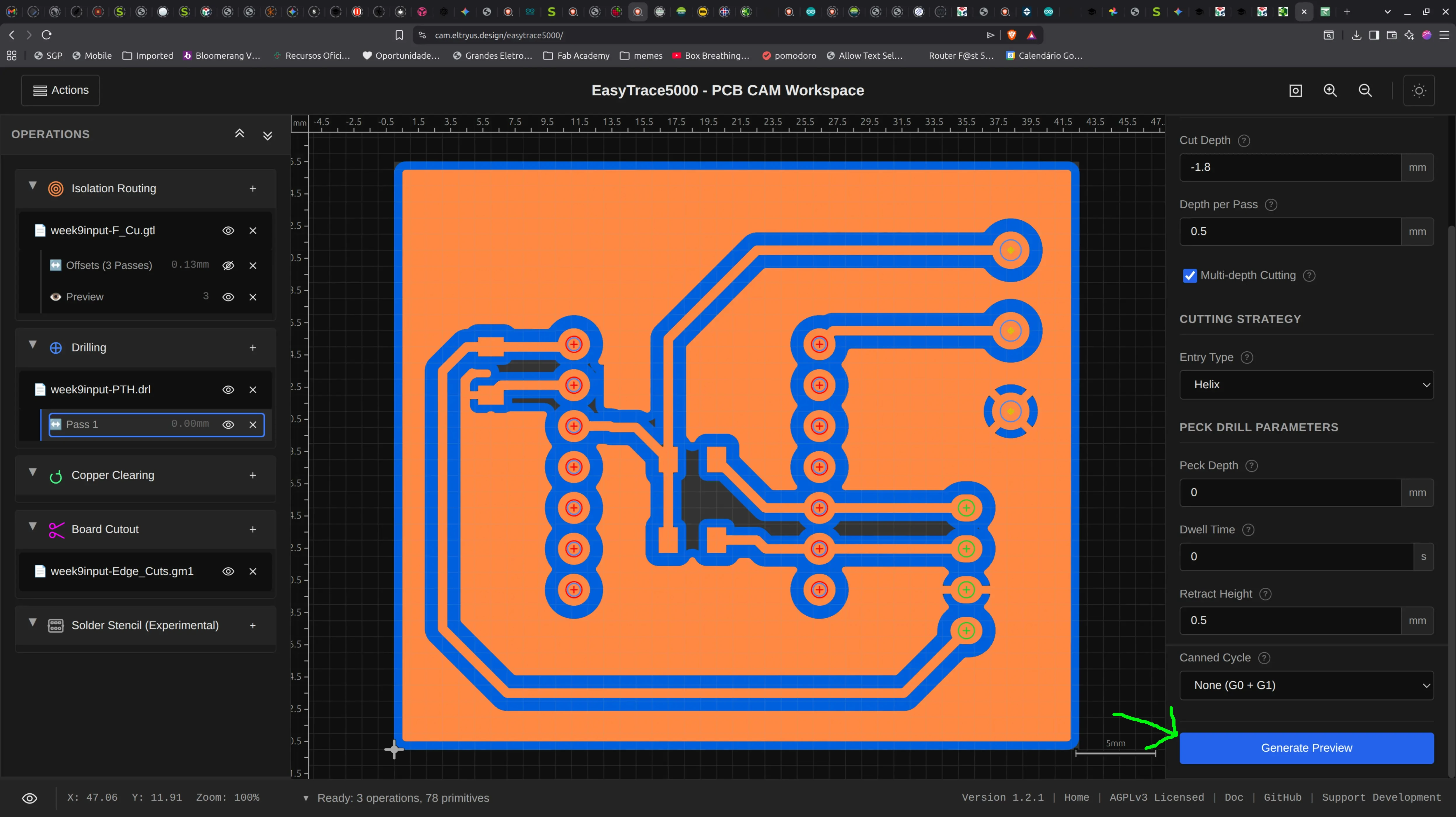
There’s a few warnings in red, as the drill is wider than the default holes, but since we already increased the pad size, it should be alright. If it showed in yellow, then it would mean the drill is narrower than the holes and the tool will draw a path to widen the holes.
We then click on “Export Manager”:
We deselect the “isolation” operation, because we just want to do drilling now.
We click “Calculate toolpaths” and then “Export files”. A file “pcb-output-drill-week9input-PTH.nc” is saved.
We can check that file again in ncviewer:
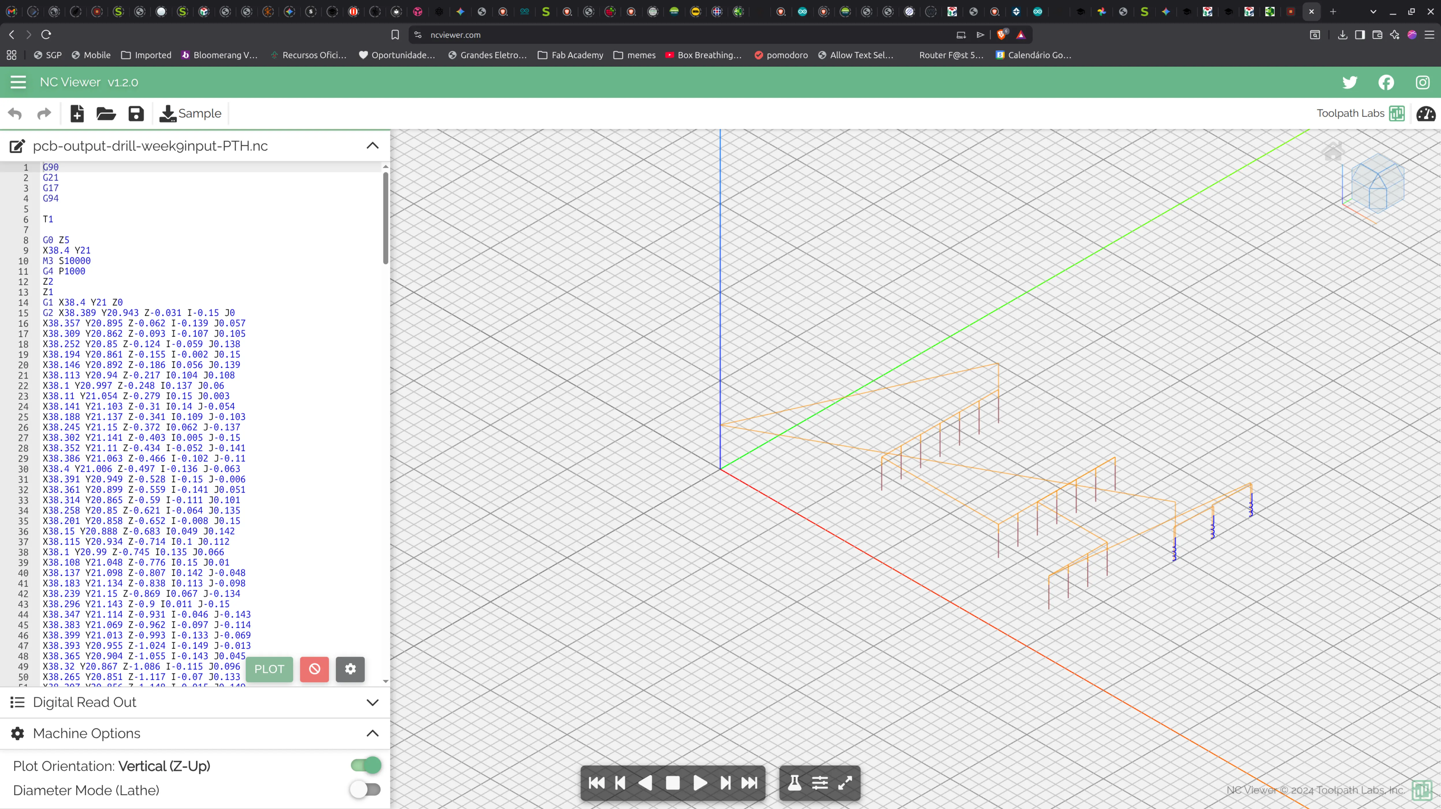
We can see on the right that the bigger holes will be done with an helix movement.
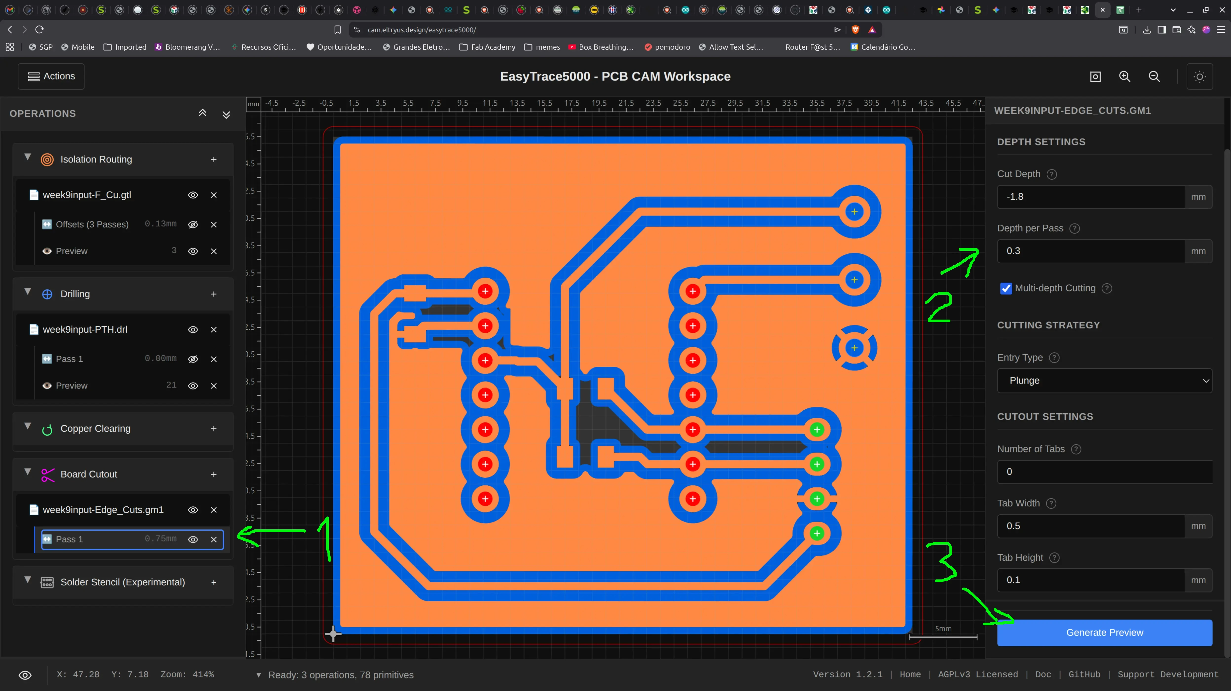
Finally we go to Easytrace5000 again and click on the “Board cutout” preview file and select a tool of 1.5 mm diameter, because it will be a different mill than the one used for drilling the wholes. We leave other parameters as defaults and click “Generate Cutout path”:
We could change the “Depth per pass” to 0.6 mm to be faster, but let’s err on the safe side and leave the default as 0.3 mm.
We click “Generate preview” and then “Export manager:
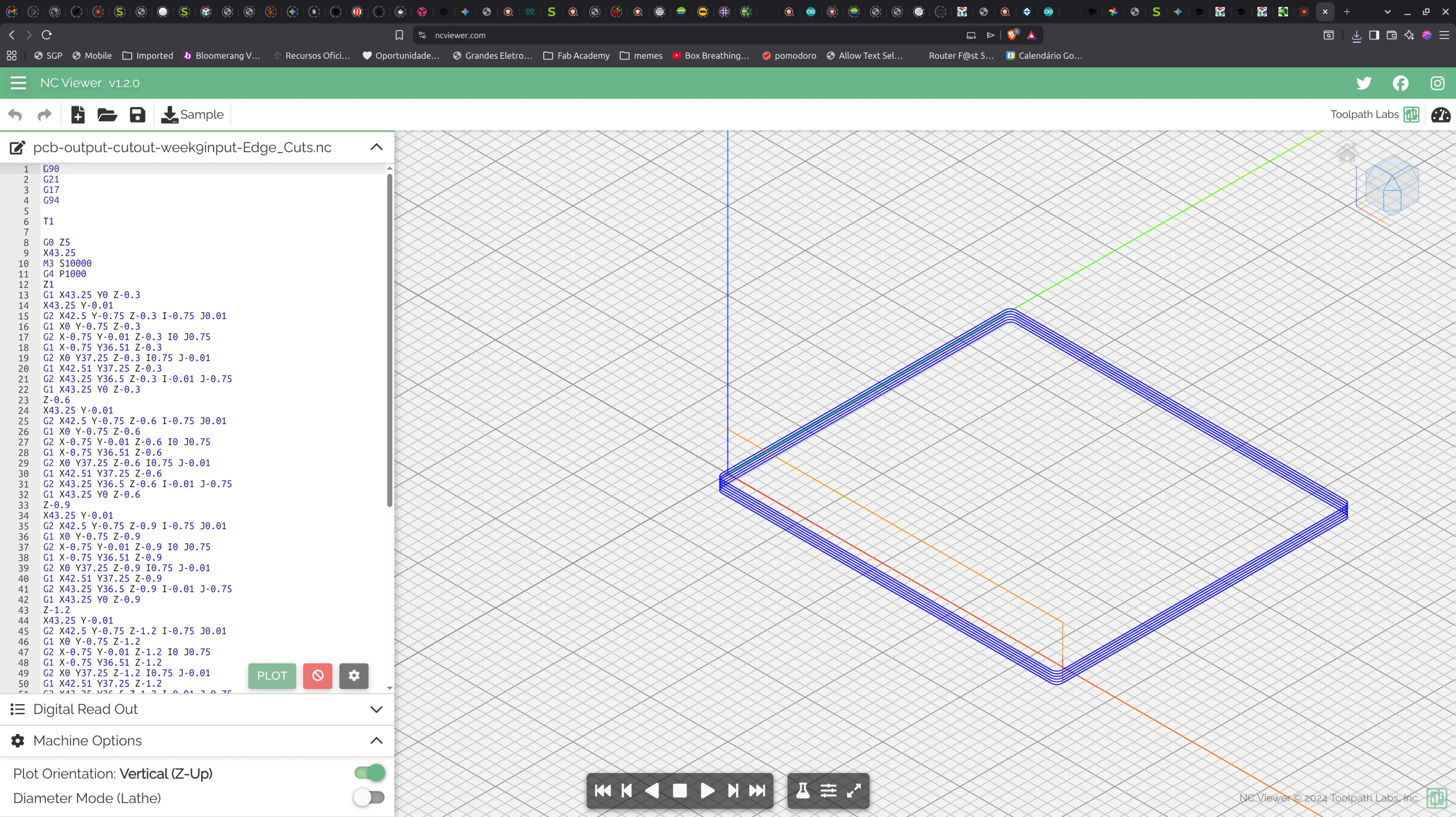
We deselect every operation except the “cutout”, click “Calculate toolpaths” and then “Export files”:
A file “pcb-output-cutout-week9input-Edge_Cuts.nc” is saved, and we also check it in ncviewer:
Milling the board with Candle
Candle is available for linux and supports the Desktop CNC that we have.
We load the “pcb-output-isolation-week9input-F_Cu.nc” file and can see a preview of the board at the top.
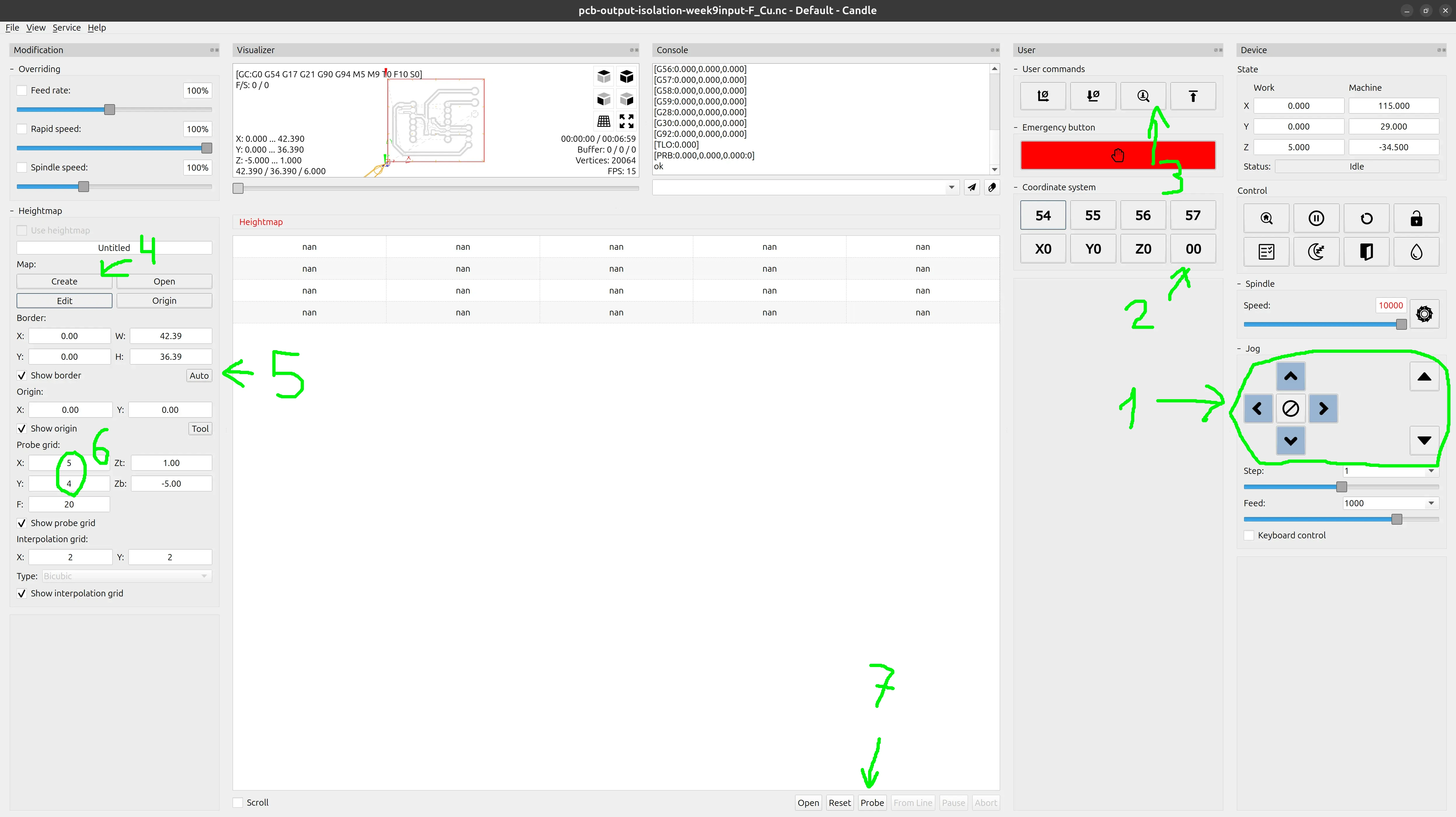
We use the controls (1) on the right to place the end mill where it is going to start milling, corresponding to the origin of our board (the bottom left previously defined), set the origin (2) and do a quick Z probe (3) just in case.
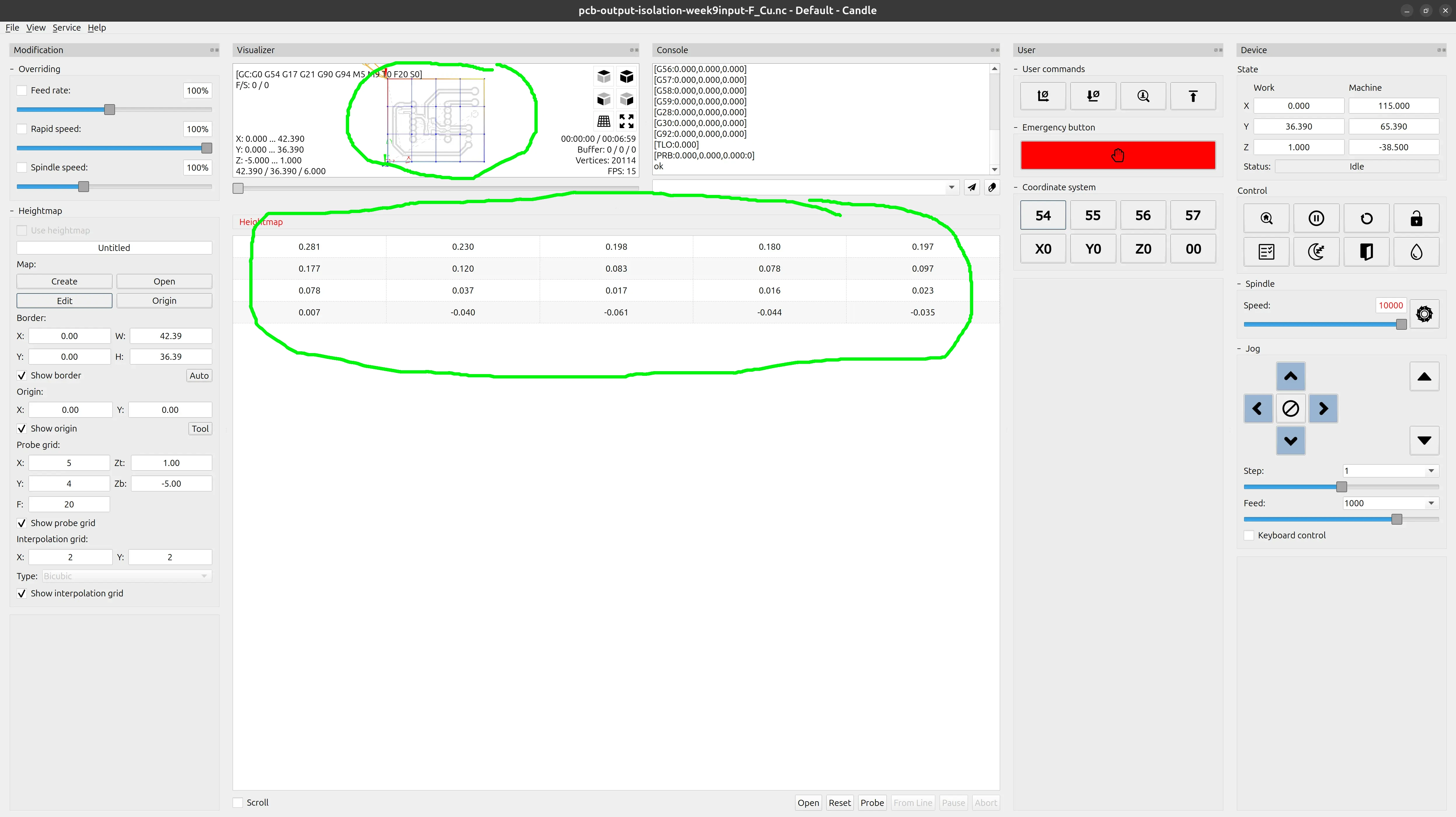
It’s then recommended to create a heightmap, because there are micro differences in the height of the board, and not doing so might result in taking more or less material than we should.
We do that by clicking the “create” button (4) and click the “auto” button (5) to aquire the board dimensions automatically. After that we define the number of horizontal and vertical probes we want along the board dimensions (6) and finally click “probe” (7)
It begins probing:
Sticking the end mill too deep
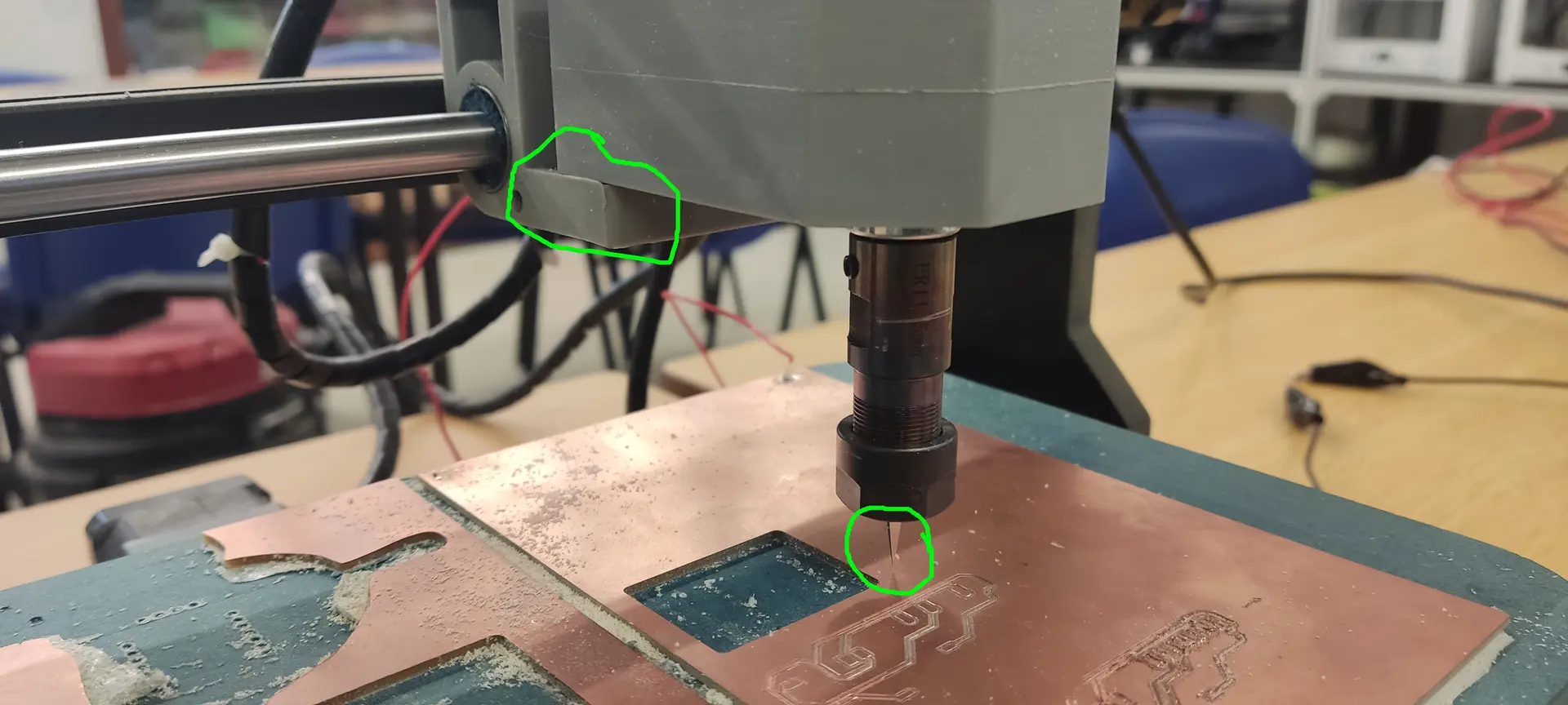
Before I got this working, I thought that I broke the Z probe process, because it was not working. It turns out that I had stuck the end mill too deep into the collet, and when moving the mill in the Z axis, the motor would try to drive the end mill into the board but it would never reach it !
So I had to untighten it and move it closer to the board.
We can then see that it has created a grid along the board, and we see that indeed there are height differences:
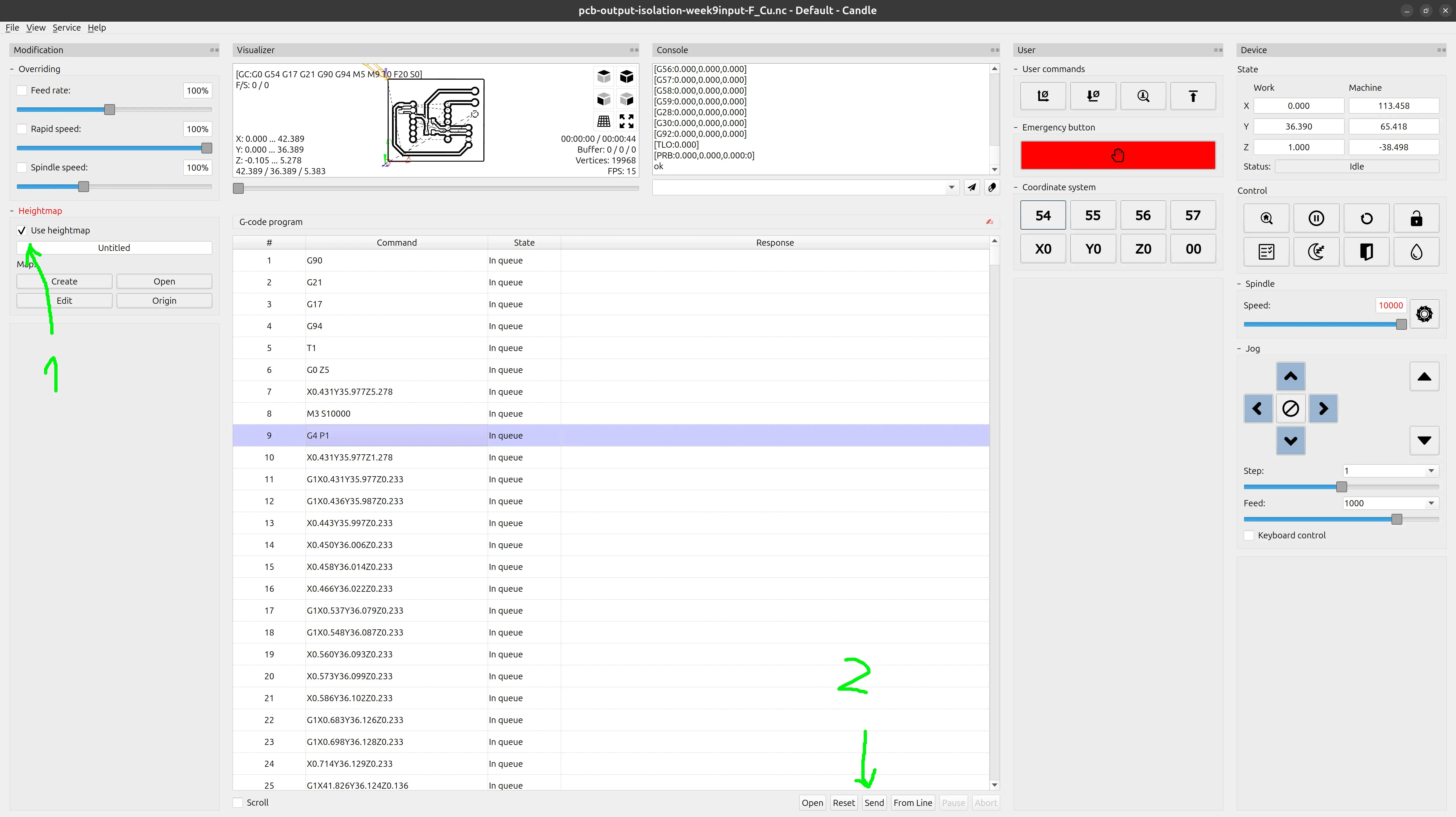
Confusingly, once the height map is created, the checkbox to use the height map is not enabled automatically, so we have to enable it ourselves (1) (otherwise the height map will be ignored), and we’re ready to start milling by clicking “Send” (2)
Remove the Z probe wires of the mill !
A common mistake was forgetting to remove the probing clamp and wires from the end mill before starting to mill. The mill will start spinning at great speed and it will roll the wires around it and it can damage them, the clamps or the connection to the controlling board, so make sure to remember to remove them !
This was the process for the more delicate milling of the board tracks. Next we need to change tools to the drill to make the through-holes and change again to another sturdier (and wider) mill to do the final cutting. Each time we load the respective nc file and do just one Z probe to determine the height of the tool, but we don’t need to repeat the height map process because both processes are meant to go through the whole board.
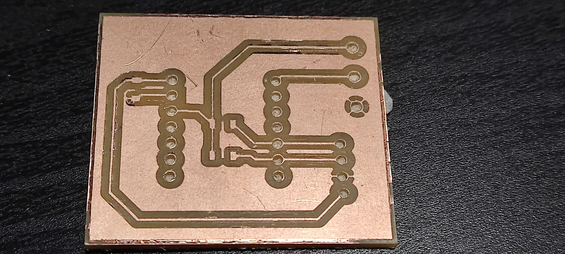
Final board
Here’s what the board looks like:
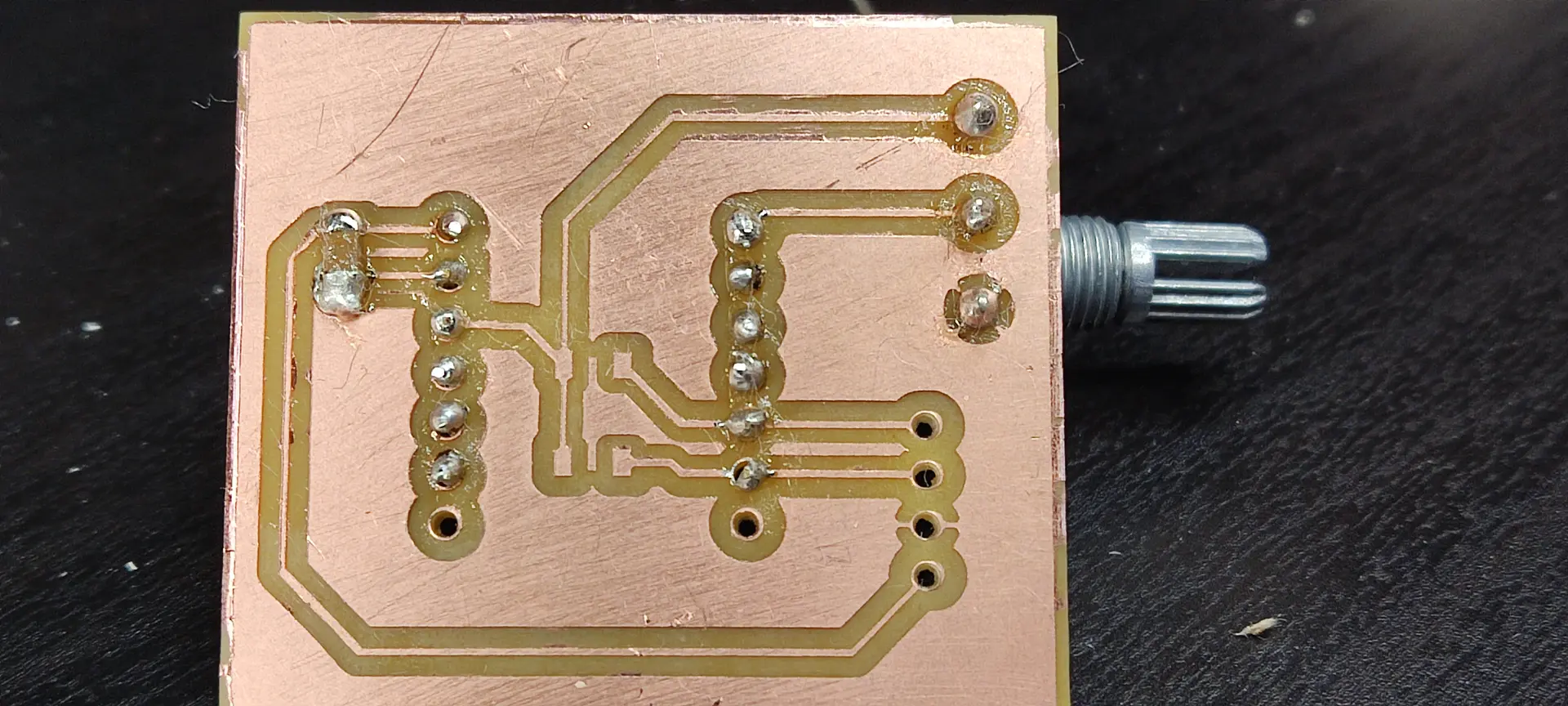
And here’s with the the basic components soldered:
and from the other side:
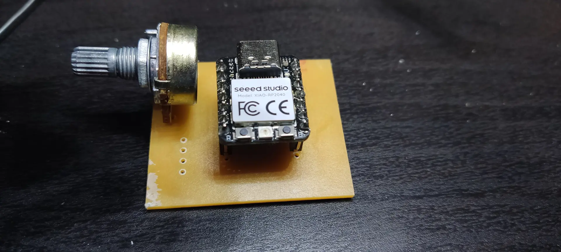
Notice a couple of things:
- We were out of 7 pin female headers, so I used available 6 pin headers. That’s OK because I didn’t need all the pins 😅
- I didn’t yet solder the connectors and pull up resistors because I’ll only need them later for the communication assignment. I’ll deal with that later.
Testing the board
I used the “AnalogReadSerial” sample sketch that with Arduino IDE, but targeted the Xiao RP2040:
/*
  AnalogReadSerial

  Reads an analog input on pin 0, prints the result to the Serial Monitor.
  Graphical representation is available using Serial Plotter (Tools > Serial Plotter menu).
  Attach the center pin of a potentiometer to pin A0, and the outside pins to +5V and ground.

  This example code is in the public domain.

  https://docs.arduino.cc/built-in-examples/basics/AnalogReadSerial/
*/

// the setup routine runs once when you press reset:
void setup() {
  // initialize serial communication at 9600 bits per second:
  Serial.begin(9600);
}

// the loop routine runs over and over again forever:
void loop() {
  // read the input on analog pin 0:
  int sensorValue = analogRead(A0);
  // print out the value you read:
  Serial.println(sensorValue);
  delay(100);  // delay in between reads for stability
}
I just changed the delay from 1 to 100 ms so I could see the value change slower.
The value read ranges from 0 to 1023, and is proportional to the voltage being read, which in turn is proportional to the angle of the potentiometer shaft.
This prints the result to the Serial Monitor and I also used the Serial Plotter tool to show the result.
This is the board working: