Electronics design using KiCad
Although slightly outdated, I mostly followed this tutorial:
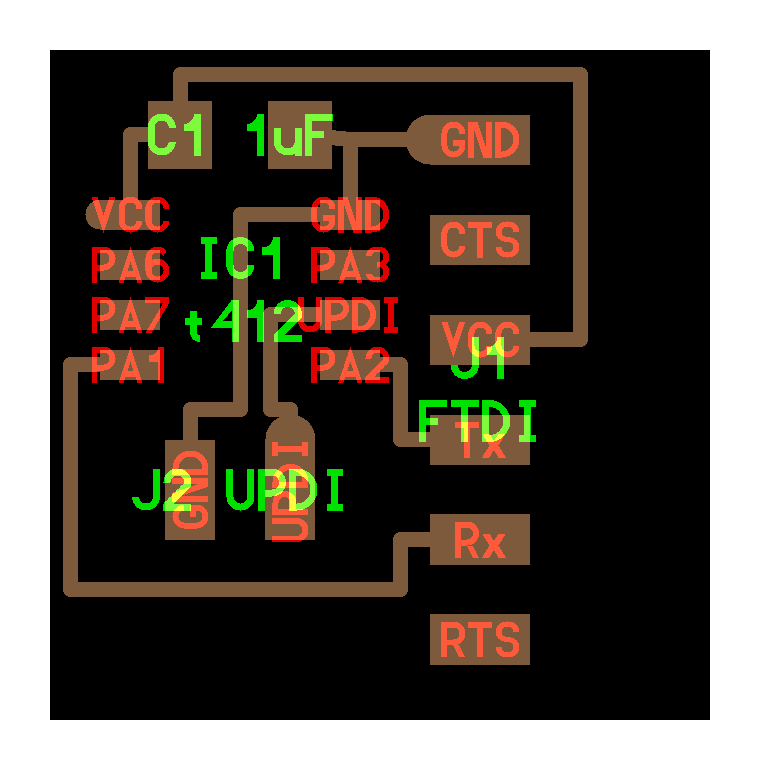
It uses as inspiration Neil’s ATTiny412 echo board and adds a button and LED.
The main challenges were:
- tutorial was done on KiCad 5.1 but the most recent is 9.0. Some stuff was moved around, renamed or just doesn’t work the same
- The fab library components have also evolved and I had to pick some that looked similar enough
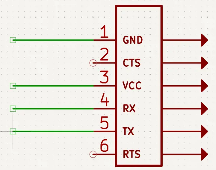
- The FTDI component that is in the library has swapped RX and TX, so I had to do routing differently and get creative with wire crossing
Mistakes found
- During review with the global evaluator, we noticed I didn’t pair the TX with RX, and vice versa. The tutorial actually does the same mistake, but there was a follow up video acknowledging this that I hadn’t noticed
- On the other hand, the FTDI component from the fab lib also has RX and TX swapped, which is probably a bug in the lib. The component does not have a datasheet, so this could not be veriefied.
- So, it can be the case that one error cancels the other and the board might be correct after all !
Step 1: Installation and Library Setup
First, you need to download the KiCad software from its official website. At the time of writing, the latest is version 9.0.7.
Next, you should download the Fab electronics component library for KiCad, which contains the electronic symbols and footprints used in FabAcademy.
I followed the instructions in the tutorial.
Step 2: Creating the Schematics
Create a new project, which will automatically generate both a schematics file and a PCB file. In the schematics editor:
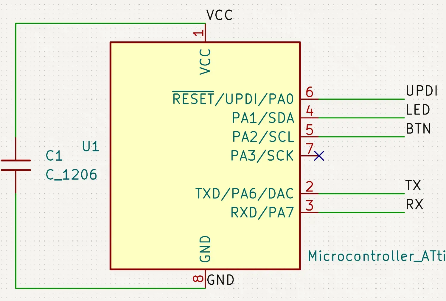
- Add components (such as microcontrollers, capacitors, resistors, buttons, and LEDs) by pressing the ‘a’ key and searching for the part.
- Draw wires to make electrical connections by pressing ‘w’. To avoid an ugly spider net of crossing cables, use labels (press ‘l’) to create invisible connections for common nets like VCC, GND, TX, and RX.
- Add power flags to explicitly specify where the power inputs (like ground and VCC) come into the circuit.
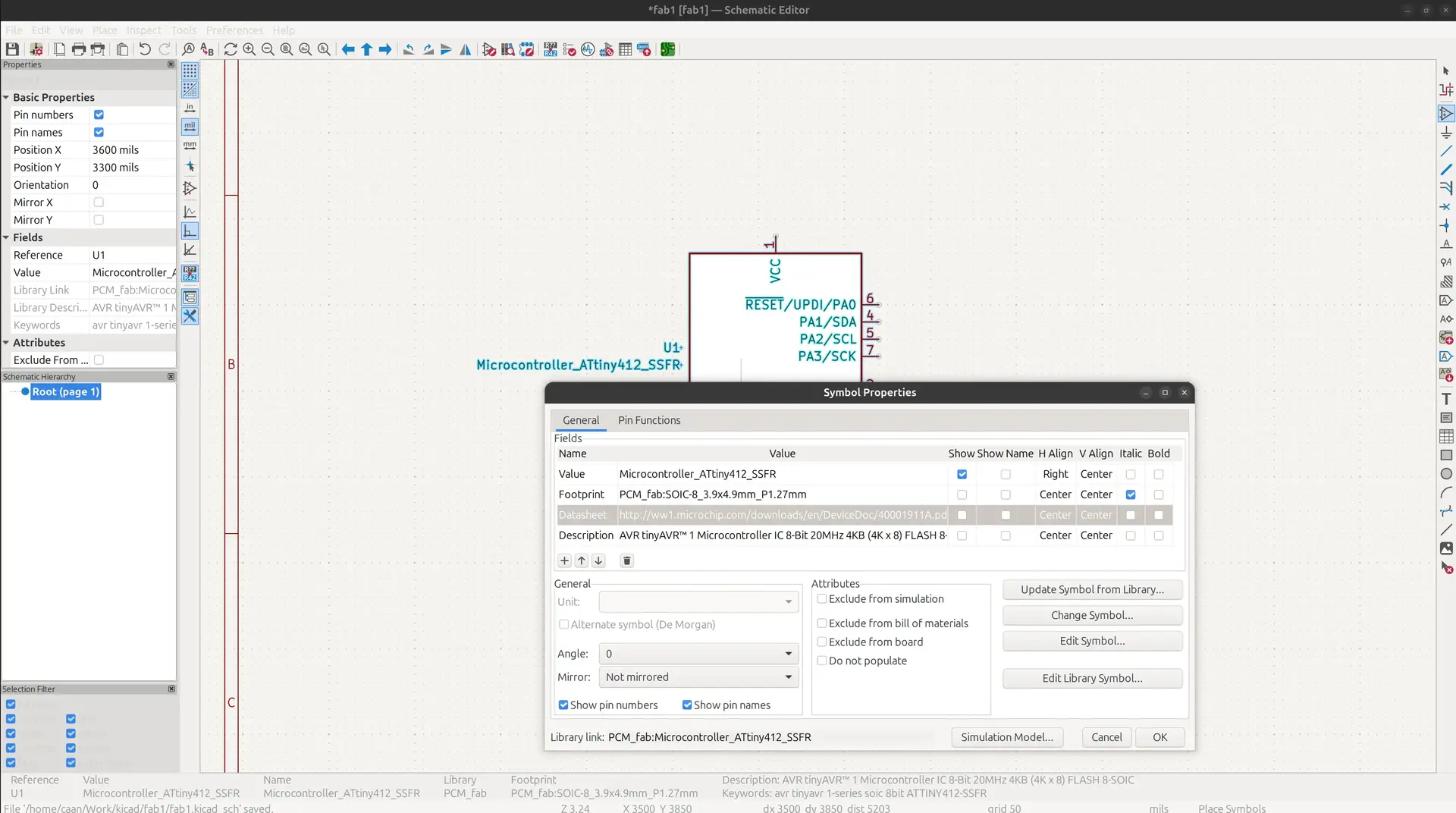
- Annotate the schematic symbols so KiCad assigns unique designator numbers to each part (for example, changing question marks into C1, U1, etc.).
- Run the Electrical Rules Check (by clicking the bug icon) to verify that there are no missing connections or electrical errors in your drawing.
Adding components
I added the following components.
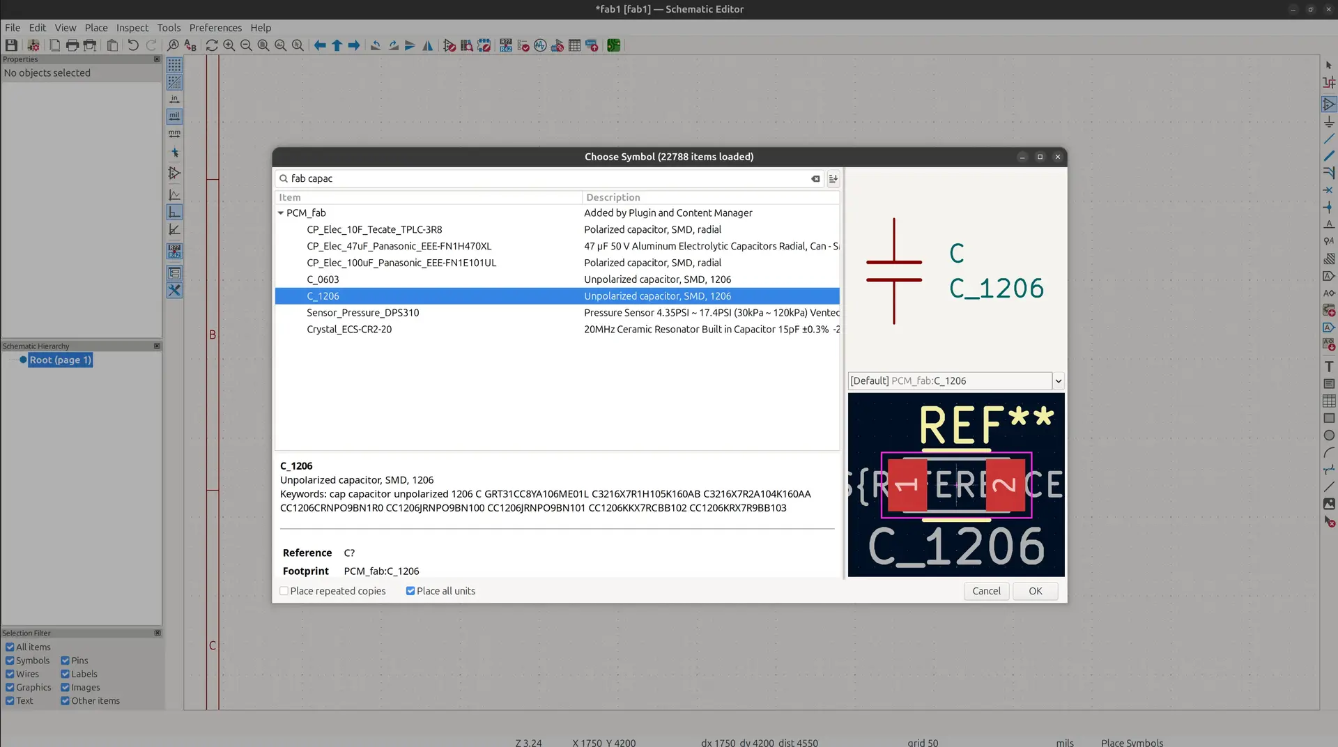
For the variants, I picked the “1206” as they are easier to hand solder.
This is the list of components:
| Reference | Value |
|---|---|
| C1 | C_1206 |
| D1 | LED_1206 |
| J1 | Conn_PinHeader_UPDI_1x02_P2.54mm_Horizontal_SMD |
| J2 | Conn_PinHeader_FTDI_1x06_P2.54mm_Horizontal_SMD |
| R1 | R_1206 |
| SW1 | Switch_Tactile_Omron |
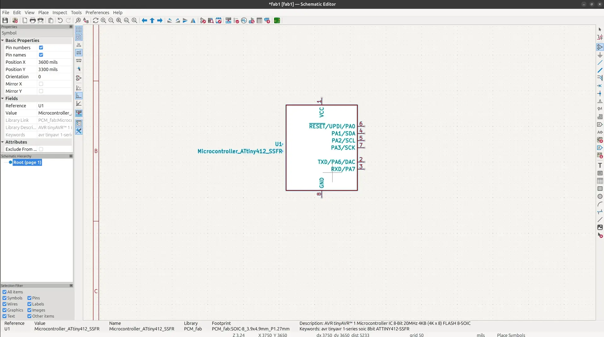
| U1 | Microcontroller_ATtiny412_SSFR |
Select the ATTiny412
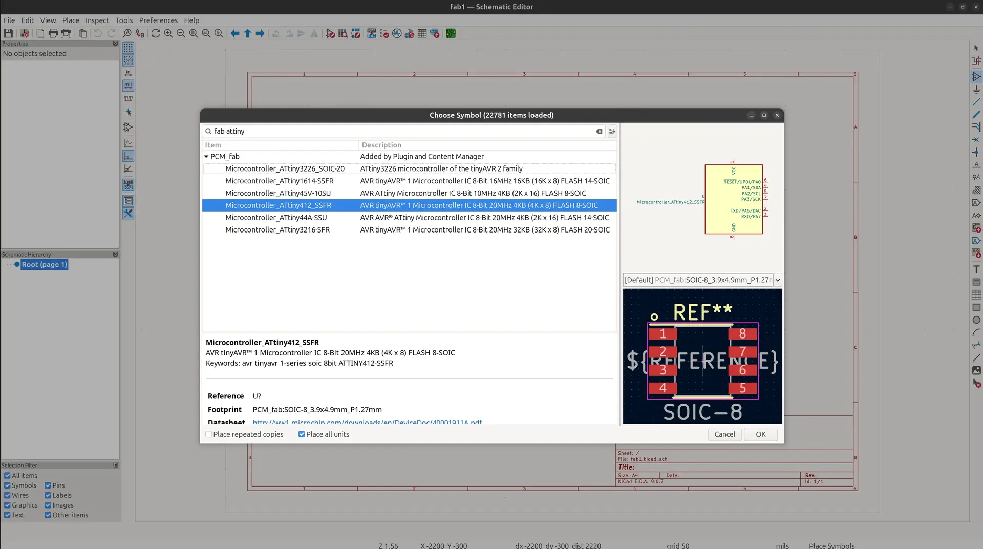
Here’s what it looks like in the schematic.
We can right click to see properties, including datasheet:
Add the remaining components, up to capacitor.
Whenever we have more than one choice I went for the ones that end in “_1206” which is the form factor that is easier to hand solder.
Draw wires
We can use Place -> Draw wires or press W to connect components.
One can either connect the wires directly:
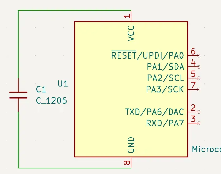
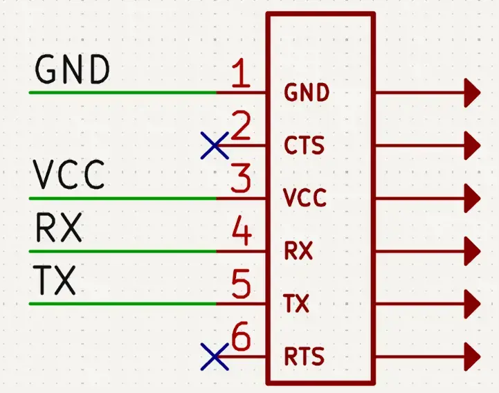
Or assign matching labels on all points that should connect. The latter avoids having a messy looking schematic.
In this case we don’t connect wires to anything:
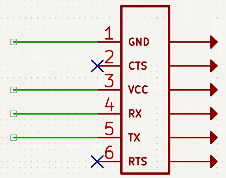
For pins that are not connected we use Place -> Place No connect Flags or just press Q
Then we add the labels with Place -> Place Net Labels or press L
To avoid confusion, we preferably use the standard names like the ones already in the schematic.
In order for this to work, we have to assign the same labels to other components, taking care that we assign such labels to the correct pins, as indicated in the schematic.
Once we assign all the labels we can try to run Inpect -> Electric Rules Checker and see if we missed something.
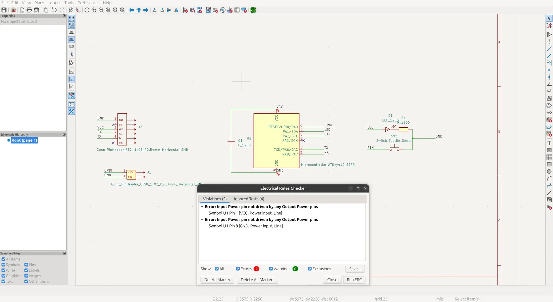
It seems we did and we fix it in the next step.
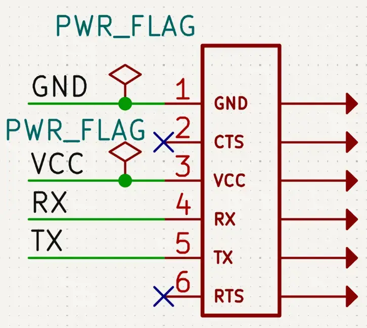
Add power flags
Despite adding the correct flags KiCad still needs to be told explicitly where the power inputs (like GND and VCC) come into. So we add it in the FTDI Component with Place -> Place Power symbols or P
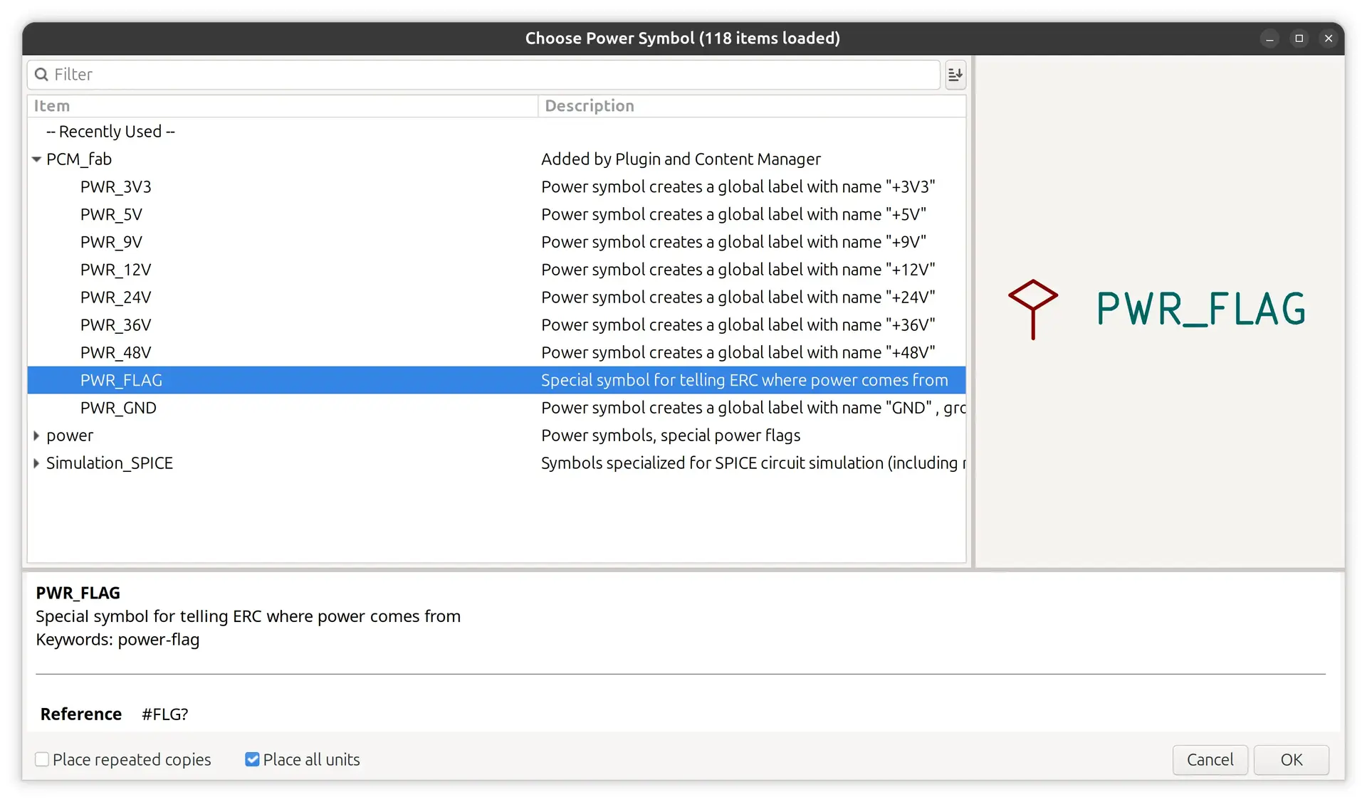
And then place it on the correct pins.
Annotate the schematic symbols
This was already automatically handled when adding components, so we don’t need to do anything else here.
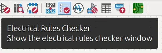
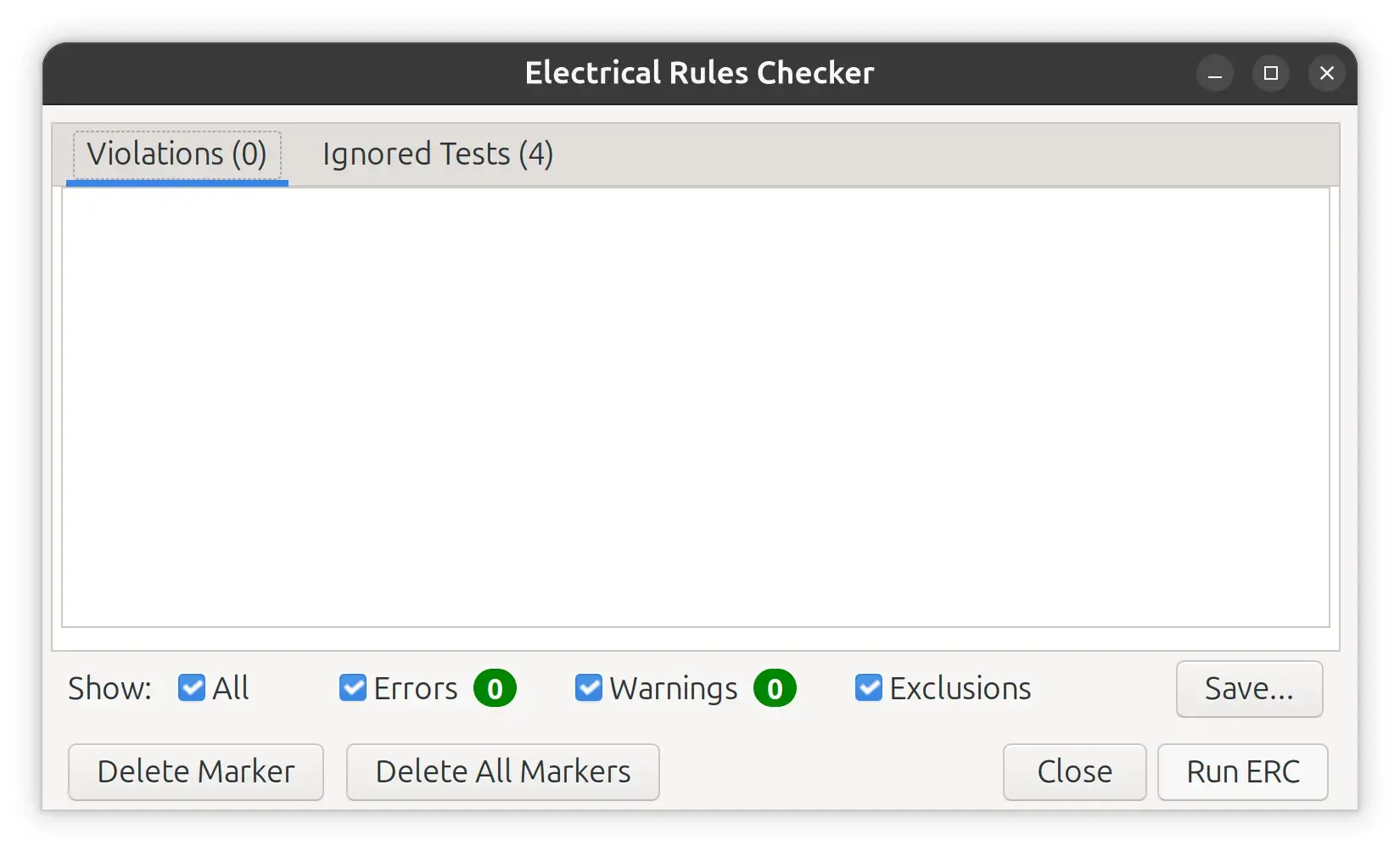
Run the Electrical Rules Check
We can now run the checks again with Inpect -> Electric Rules Checker or clicking on
And we can now see no errors:
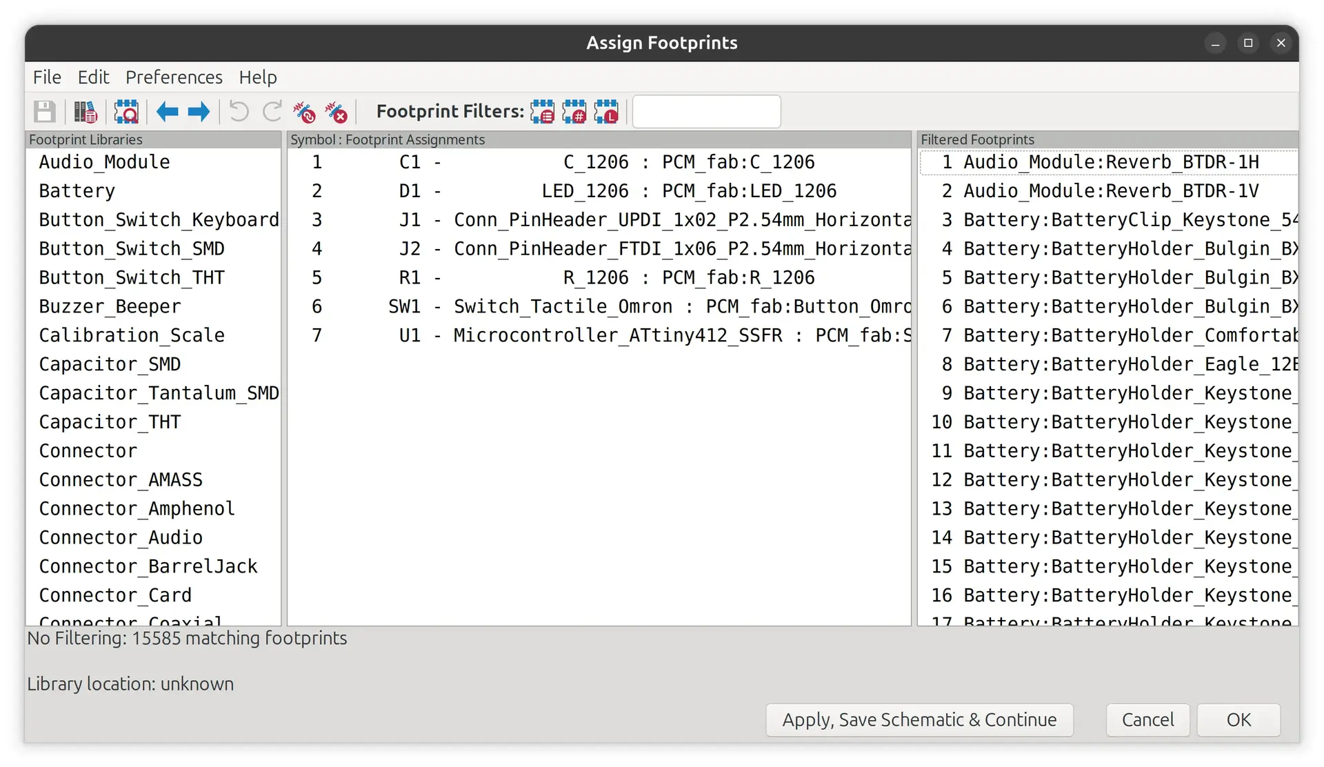
Step 3: Footprints
Schematic symbols must be linked to physical footprints for the board layout. If you are using the fab library, these footprints are already assigned by default.
We can go toTools -> Assign footprints
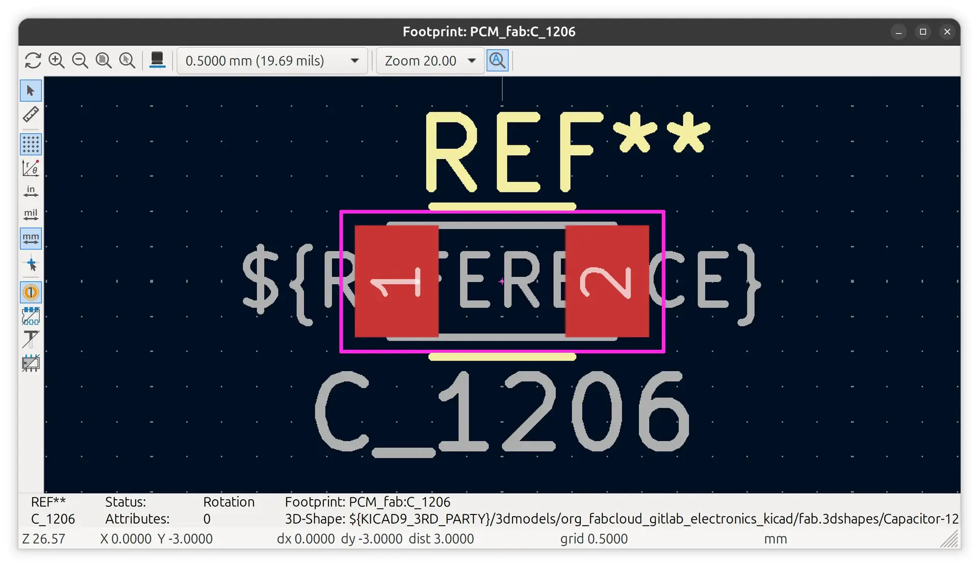
And if we Right click -> view foot print we can see the footprint of the component:
Since all components already have footprints, we’re ready to move on to the PCB
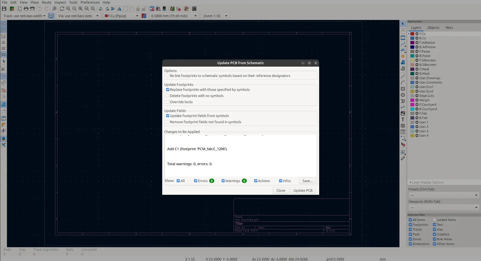
Step 4: PCB Design and Layout
We’re now ready to Tools -> Switch to PCB Editor and Tools -> Update PCB from Schematic:
In the PCB editor we will:
- Position the components logically. For instance, bypass capacitors must be placed as close as possible to the microcontroller to filter the current properly.
- Adjust the design rules: Go to the predefined sizes and set both the clearance and track width to 0.4 mm, which is the standard size for PCB milling tools.
- Route the tracks (draw the copper wires) between components, using the white guide lines as a reference.
- Create a copper fill (Add filled zones) on the Front Copper layer associated with the ground (GND) net; this connects all unconnected ground pins together and helps protect the board from electrical interference.
- Draw the board outline using the graphic lines tool.
- Run the Design Rules Check (DRC) (the bug icon) to ensure there is enough distance between all your traces and that everything is properly routed.
Position the components
The components are initially all crumbled together:
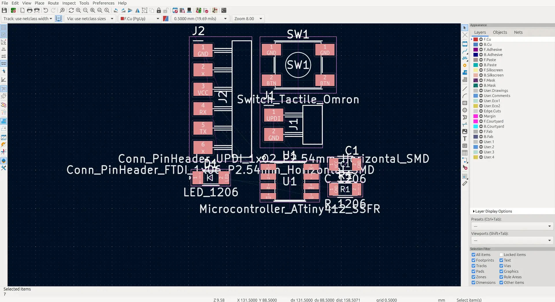
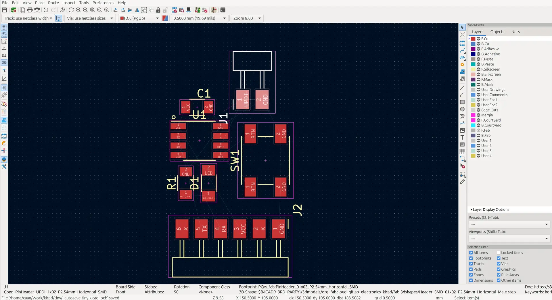
Position the components logically.
In order to have less visual noise, when moving components around, I disabled the F.Lab layer.
I rotated (R) and dragged each component to its desired position:
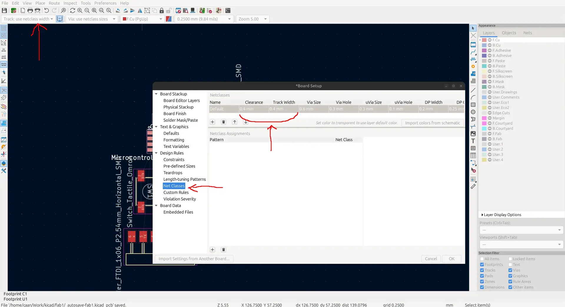
Adjust the design rules
Before we start laying out the tracks, we need to adjust some of it’s parameters.
Go to the predefined sizes and set both the clearance and track width to 0.4 mm, which is the standard size for PCB milling tools.
Route the tracks
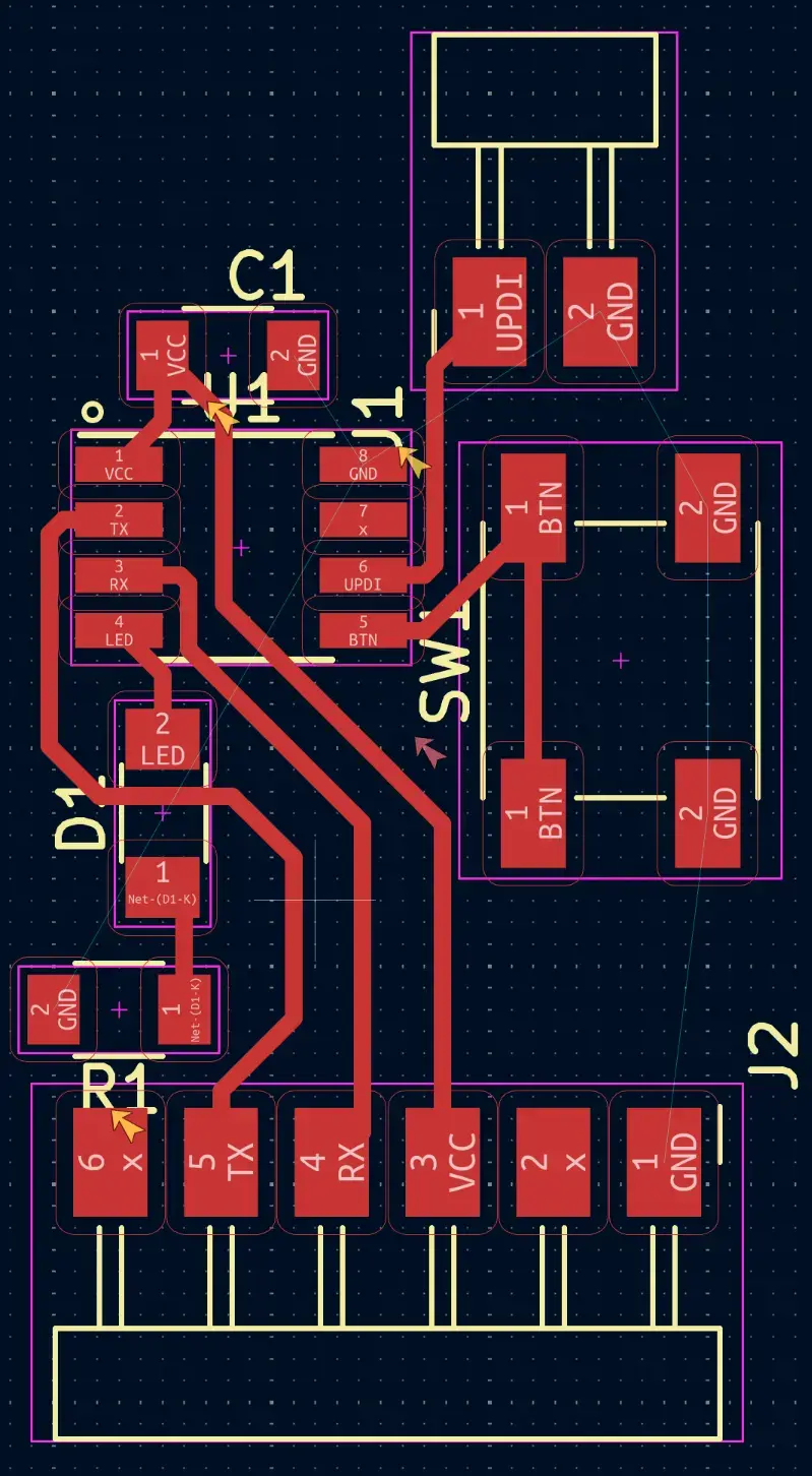
We’re now ready to draw the copper wires between components, using the white guide lines as a reference.
Press X to start routing tracks. Click one of the pins and the software will guide you to the other end of the connection.
Start with the communication lines, than VCC and then leave GND for the end.
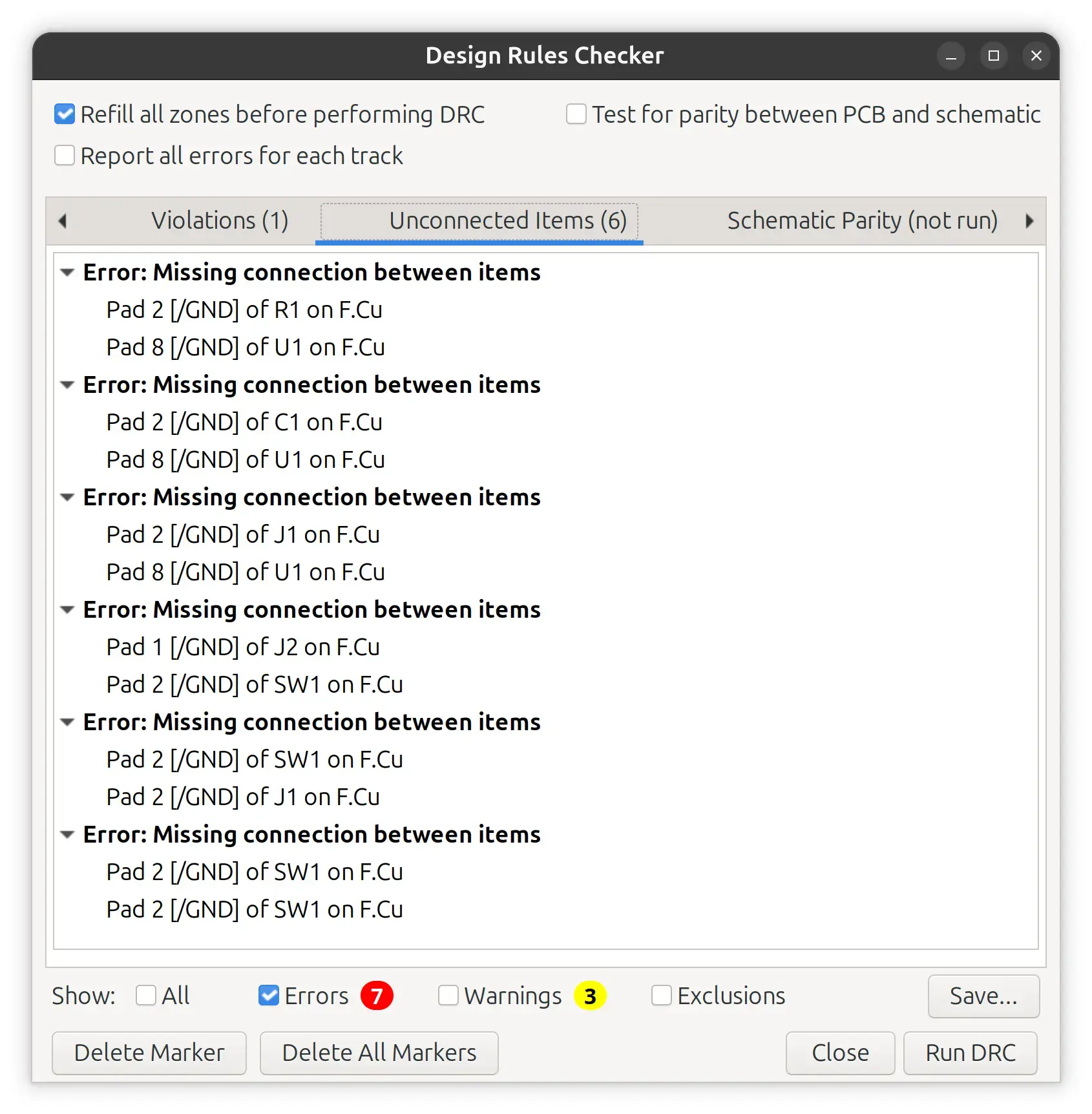
If we call the Inspect -> Design Rules Checker we can confirm that only GND is missing:
Create a copper fill
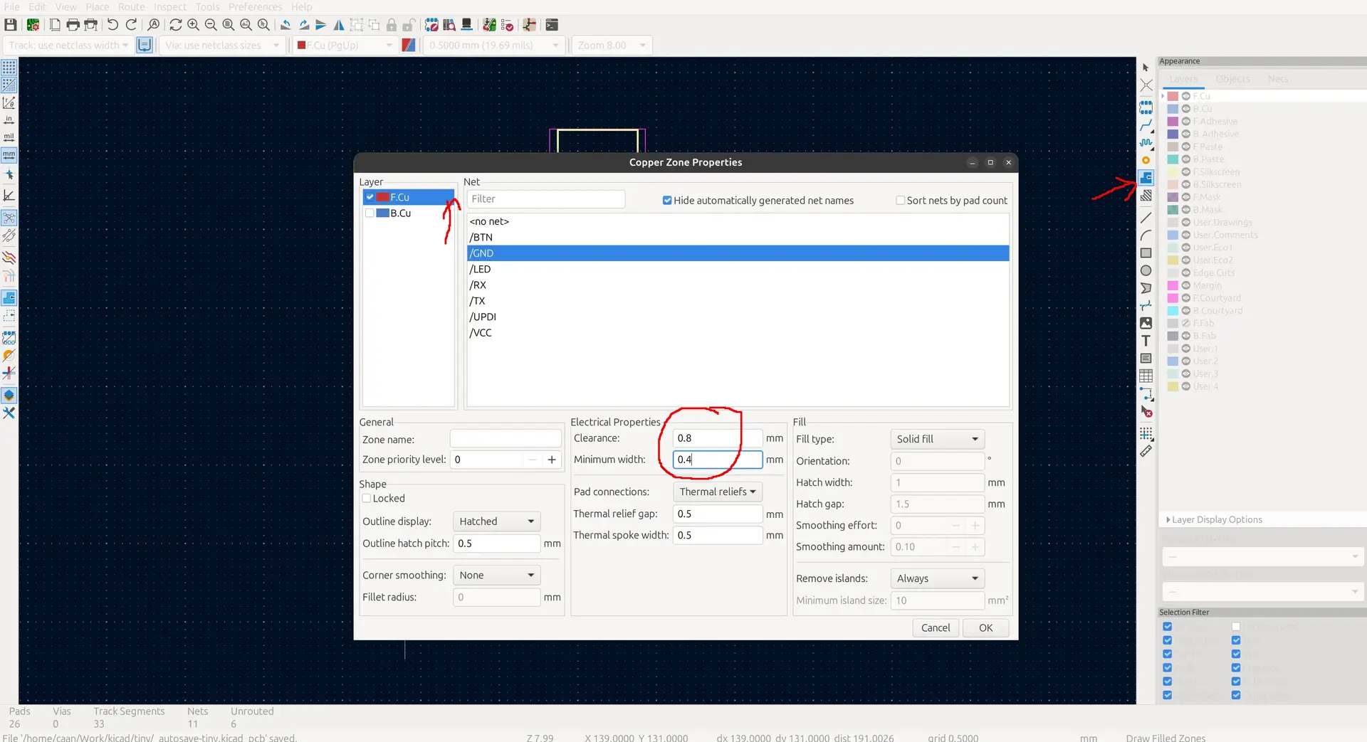
Add filled zones on the Front Copper layer associated with the ground (GND) net; this connects all unconnected ground pins together and helps protect the board from electrical interference.
We change the clearance and minimum width to 4 mm for easier milling.
Drawing the polygon around the board:
And then Edit -> Fill all zones or press B
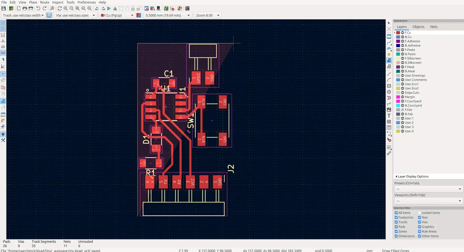
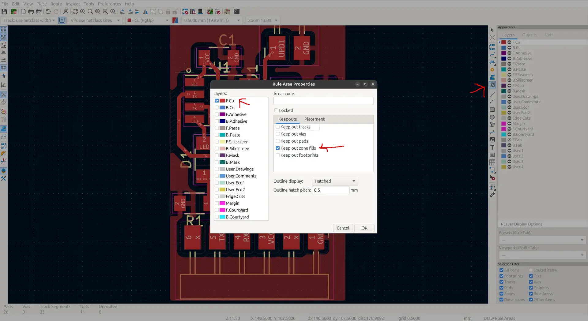
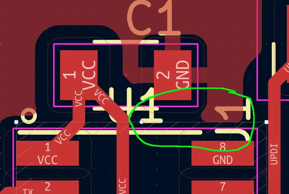
One detail, however, is that the GND is connecting directly to the microcontroller, but we would like to go “through” the decoupling capacitor. So we do this by adding special rules around the chip. We click use the Place -> Draw rule areas or click on icon on the right, and select only “keep out zone fills”. We press B again for Fill all zones
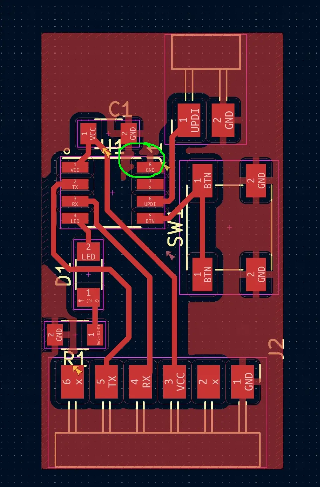
The direct connection is thus removed:
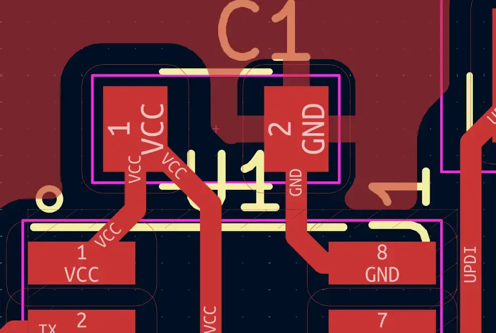
But now we need to add the wiring manually for this case:
If we run the Design Rules Checker we can confirm there are no longer any unconnected items:
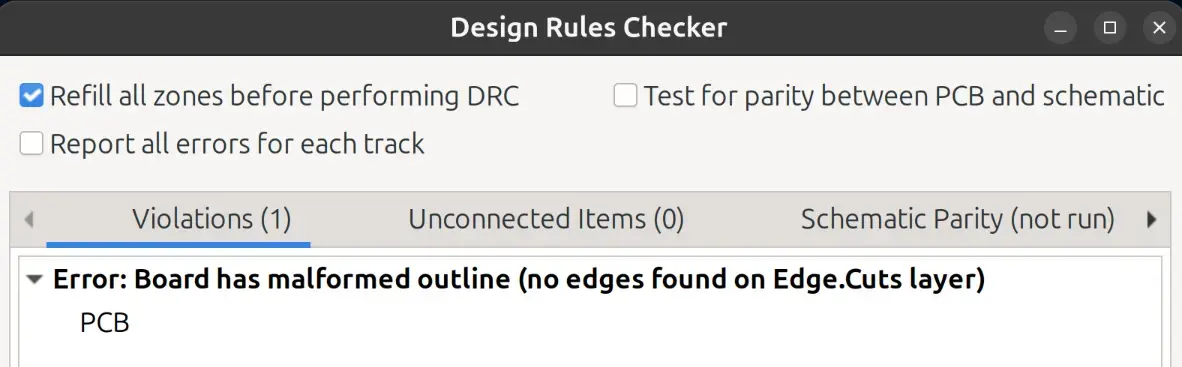
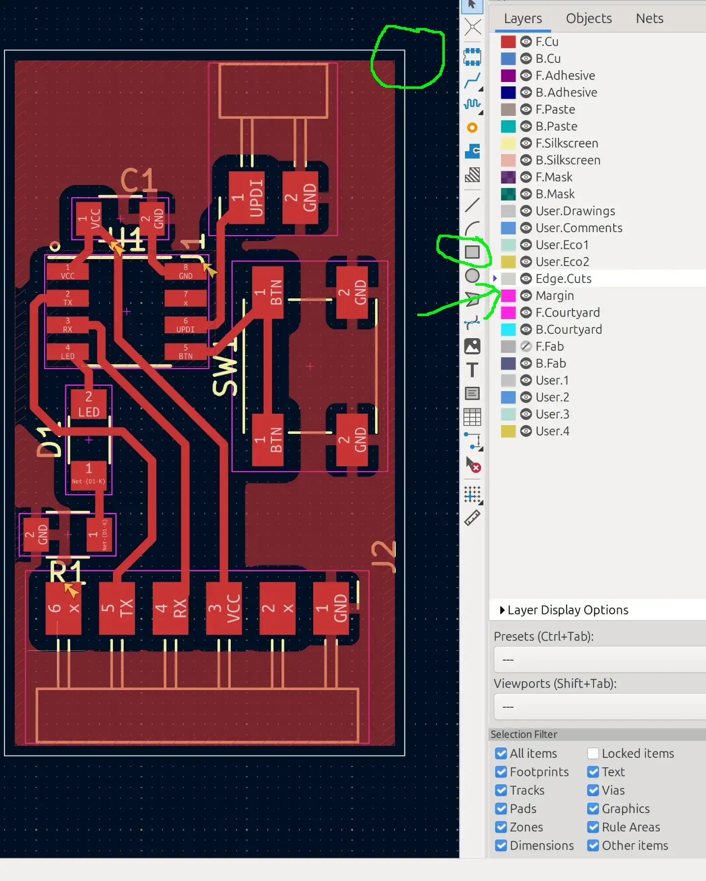
Draw the board outline using the graphic lines tool.
Basically the previous error means that KiCad does not know the boundary of the circuit. So we need to select the Edge.Cuts layer and draw boundaries, for which a rectangle was used. I left a 0.5 mm margin between the edge and the circuit so that the milling process doesn’t interfere with the rest of the circuit.
Run the Design Rules Check (DRC)
We run the DRC one last time to check:
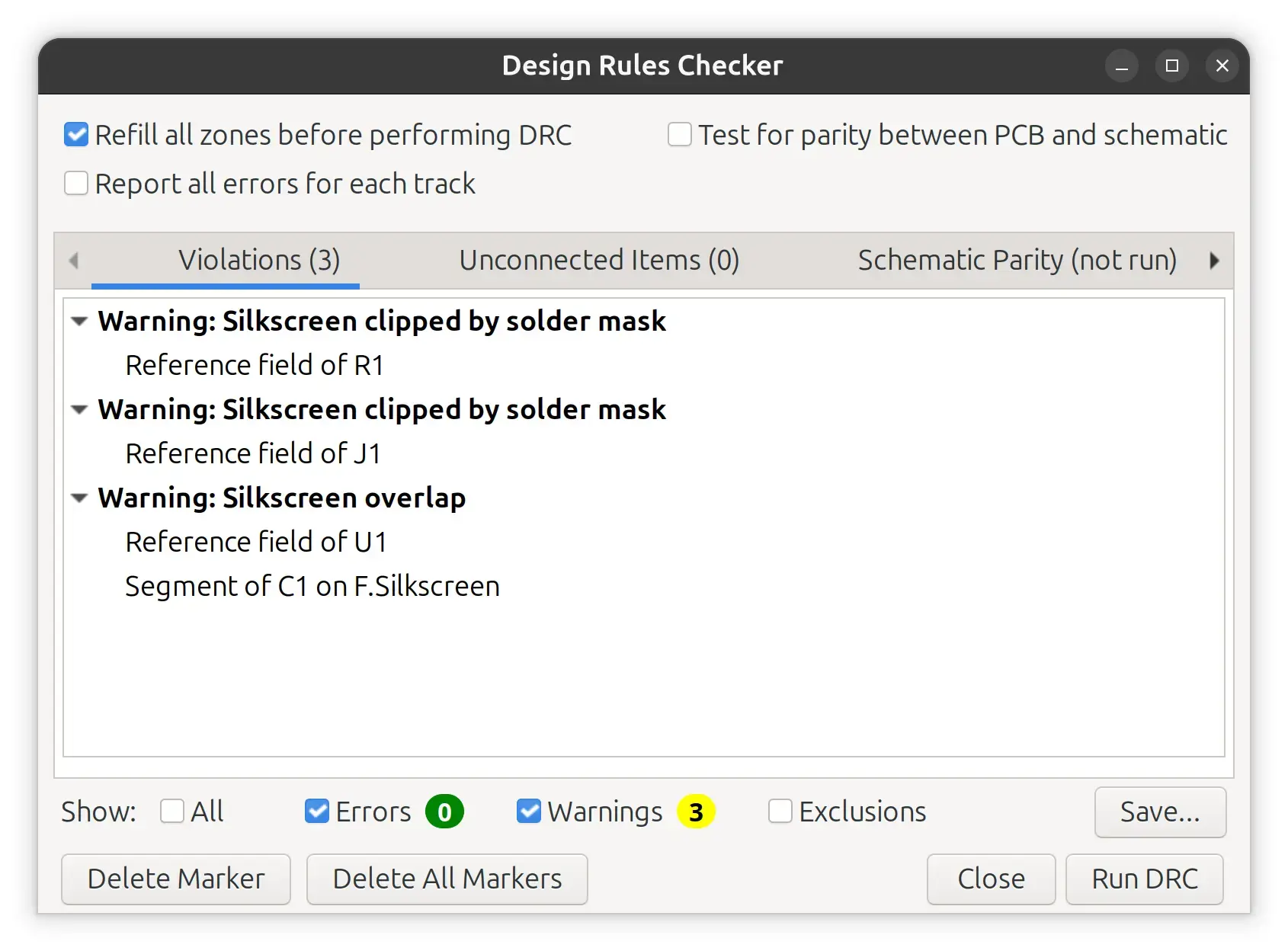
There are no more errors. There’s a few warnings about the silkscreen, but since we intend to mill the board and not send it to final production, I chose to ignore these for now.
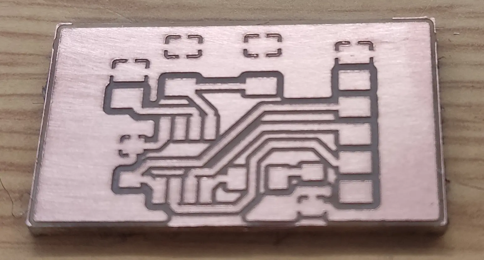
Hero shot
Here’s what it looks like after I milled it in the following week: