electronics design
Topic(s) of this week
- electronics design (video, review)
- Select and use software for circuit board design
- Demonstrate workflows used in circuit board design
Hero shots

Assignments
Group assignment
- Use the test equipment in your lab to observe the operation of a microcontroller circuit board (as a minimum, you should demonstrate the use of a multimeter and oscilloscope)
- Document the workflow for sending a PCB to a board house (leftover from Electronic Production week)
Individual assignment
- Use an EDA tool to design a development board to interact and communicate with an embedded microcontroller
What I think I already know
With my media engineering background I’m quite confident to say that I know enough about this subject to get through the week without brain meltdown. I actually did this assignment already in embedded programming week, without knowing that this would be an assignment… So I documented that too.
What I want to learn
Obviously my goal is to learn something new so I’m planning to design a flexible PCB for my final project. I’ve not one that before. I also want to have a carbon layer on top of my traces, so I’ll have to design a custom layer as well (again first time). I quickly checked the design guidelines and I think I’ll have to change my current design of the pressure sensor traces, so let’s do that in a parametrical way, using Fusion 360, and try to get that into a Kicad footprint. Again first time so lots to learn this week!
SSTM planning
Supply
| Day | Supply | Tasks |
|---|---|---|
| Thursday | 08:00-09:30 (train) | read design guidelines on carbon contacts |
| 10:00-18:00 | ||
| Friday | 9:00-13:00 (fablab) | - |
| 18:00-21:00 | Learning kicad | |
| Saturday | 12:00-16:00 | flex PCB design |
| FP mechanical design | ||
| Sunday | 20:00-23:00 | FP mechanical design |
| Monday | 11:00-14:00 (fablab) | finalizing and testing flex PCB, Casting FP sensor, document |
| Tuesday | 9:00-13:00 (fablab) | testing casted FP sensor |
| 20:00-22:00 | design SAMD21 sensor board | |
| Wednesday | 9:00-12:00 (fablab) | continue designing SAMD21 sensor board |
| document | ||
| 12:00-13:00 | Local review | |
| 13:00-14:00 | Regional review | |
| 15:00-18:00 | Neil time |
Tasks
Have you answered these questions?
- Documented what you have learned in electronics design
- Checked your board can be fabricated
- Explained problems and how you fixed them.
- Included original design files (Eagle, KiCad, etc.)
- Included a ‘hero shot’
- Leave feedback in Nueval that this weekly is ready for evaluation.
WAAG session and Group assignment
Erwin gave us a workshop on Electronic design. His slides can be found here.
Kicad originates from CERN and is open source. Basically you create a schematic, pick the components you need, place them on the board and draw traces (or connect using labels)…
Keyboard shortcuts:
a -> add component
v -> set value of selected component
r -> rotate
x -> route track (=trace)
d -> in PCB editor -> drag component -> keep traces attached (new v8 feature)!
d -> in schematic editor -> show datasheet
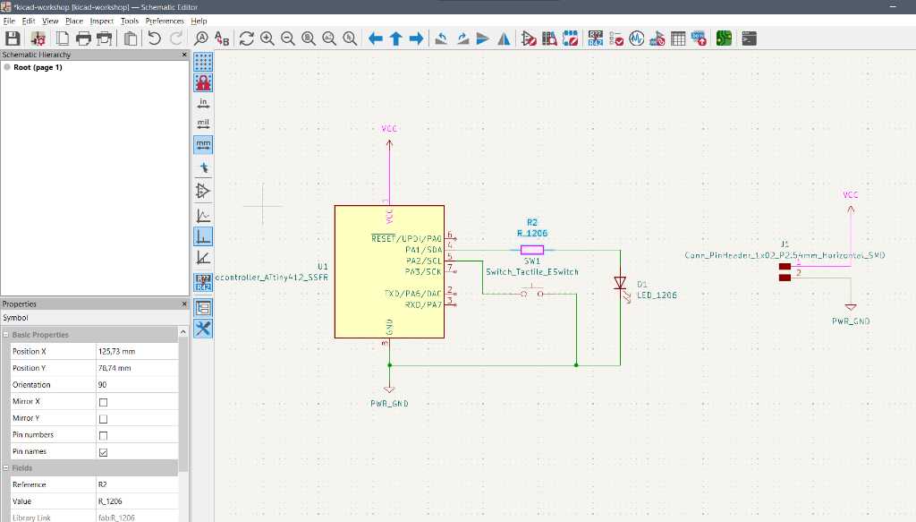
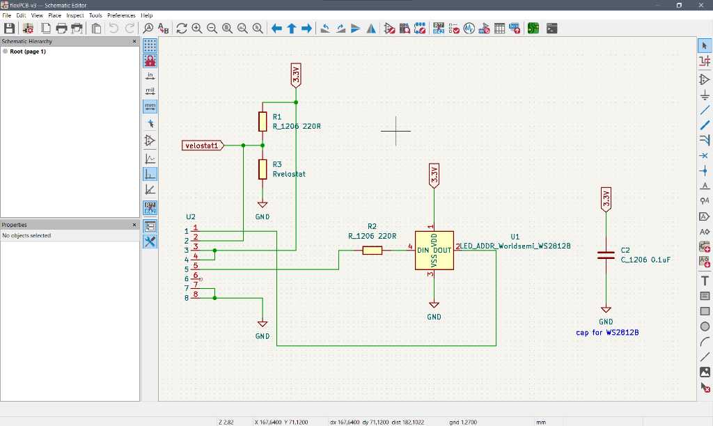
The schematic I made:
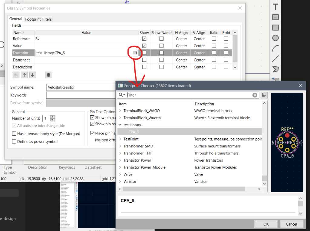
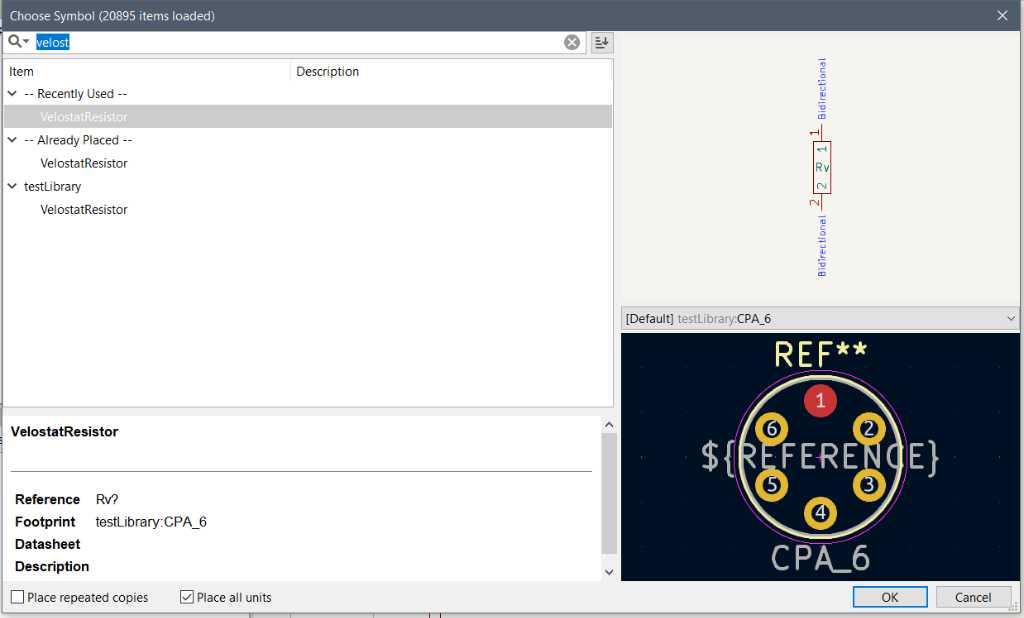
Assigning a footprint to a symbol can be done in the schematic editor -> Tools -> assign footprint:
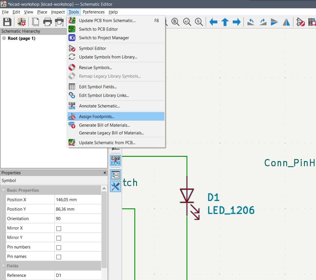
in the next screen you can select the library with footprints, select the symbol you want to edit and select the footprint you want to assign to this symbol. Click the “view footprint” button to get a preview.
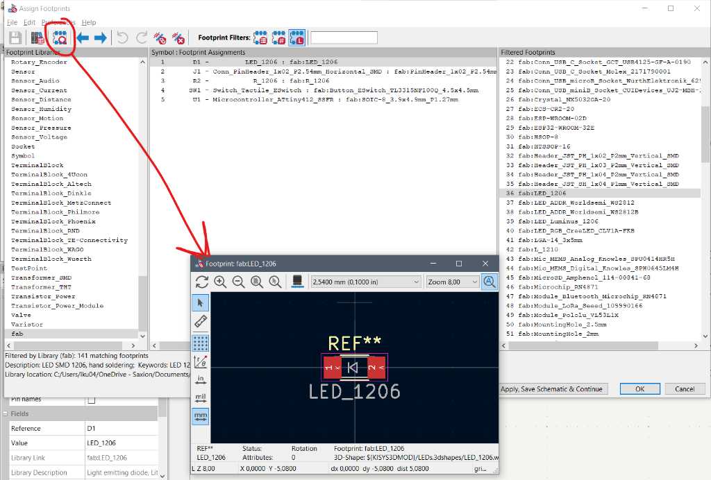
Click apply, save and continue when done and then hit OK.
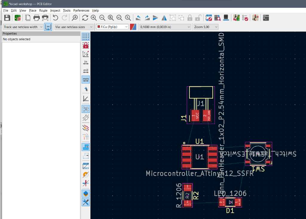
Now click Update PCB from Schematic. PCB editor is opened and you can place the components:
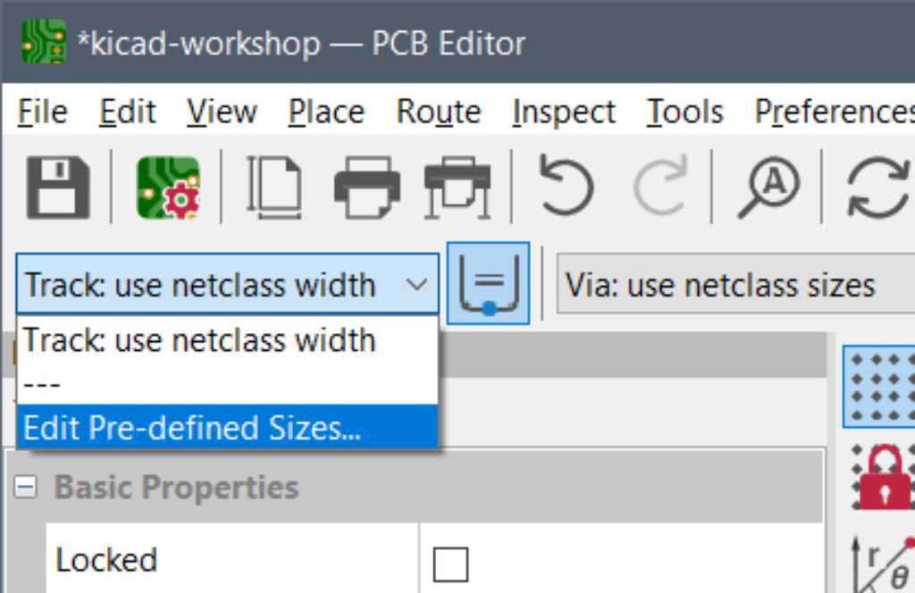
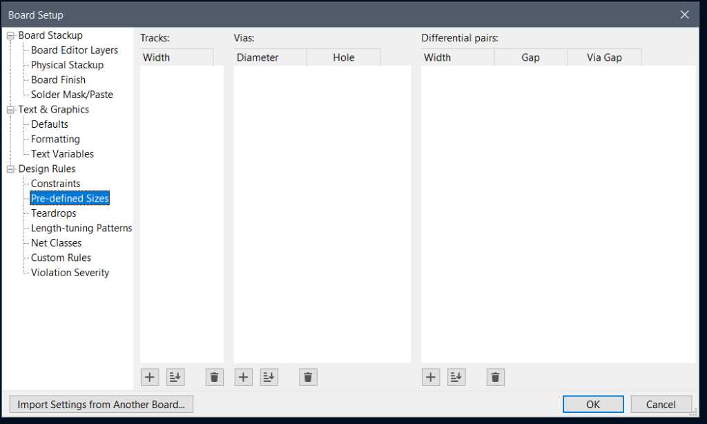
The default track size is 0.2mm which is very small, especially for Fablab milled PCBs. Changing this size is done in Edit Pre-defined Sizes.
You can now add more pre-defined sizes:
It’s even better to create a edit the Default Class because this allows you to add clearances as well:
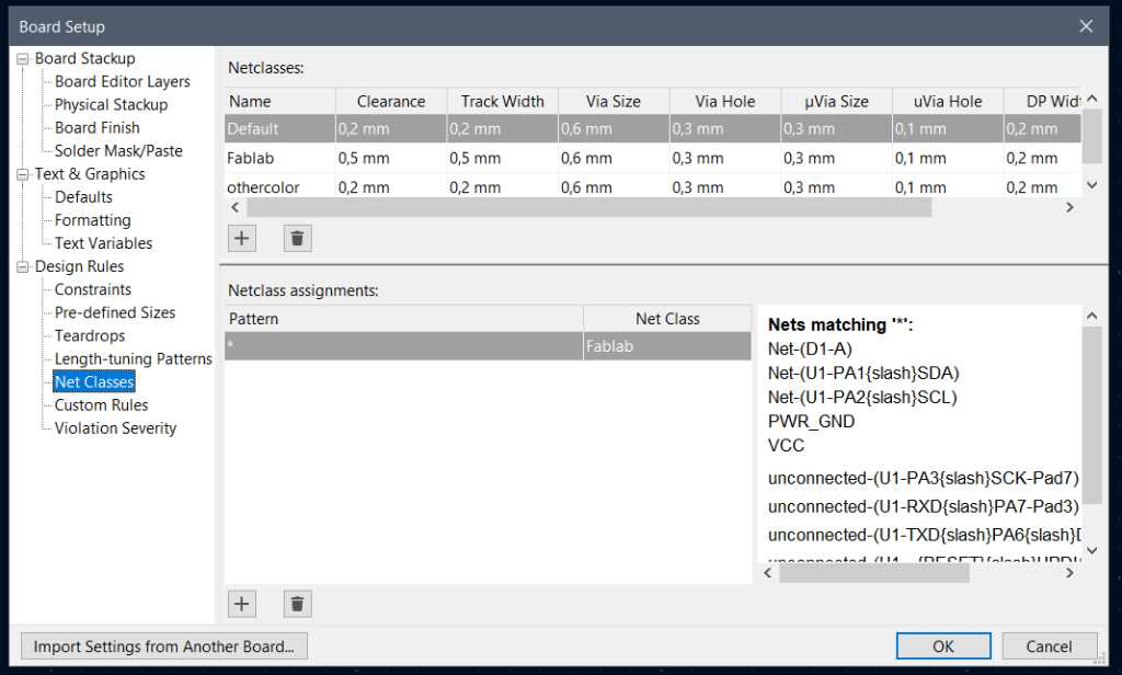
note the Netclass assignment pattern which is “*“, basically meaning to use this settings on all traces you make.
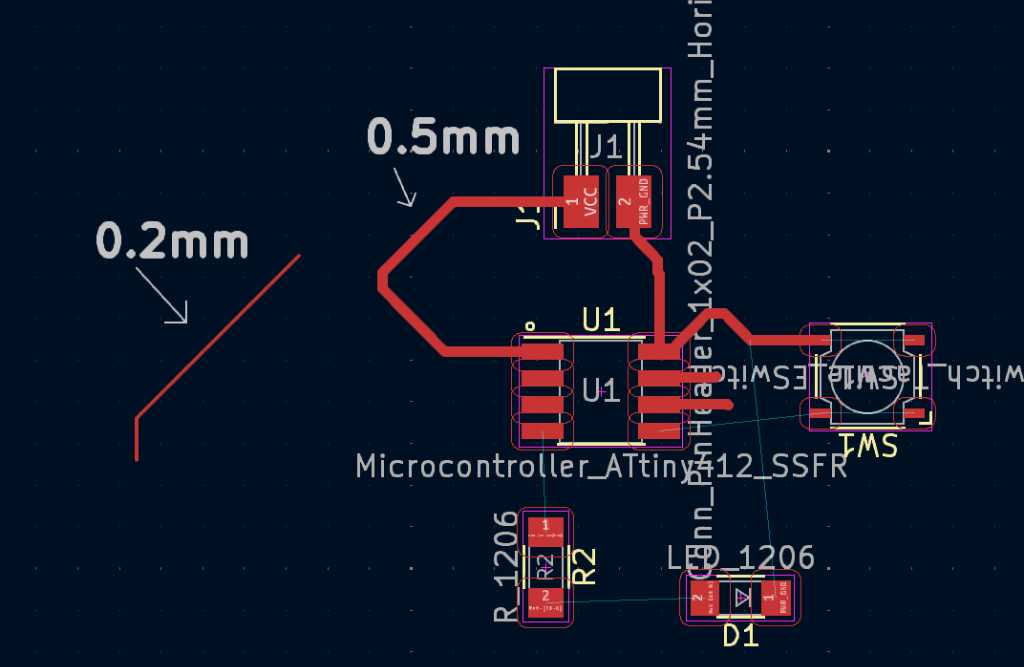
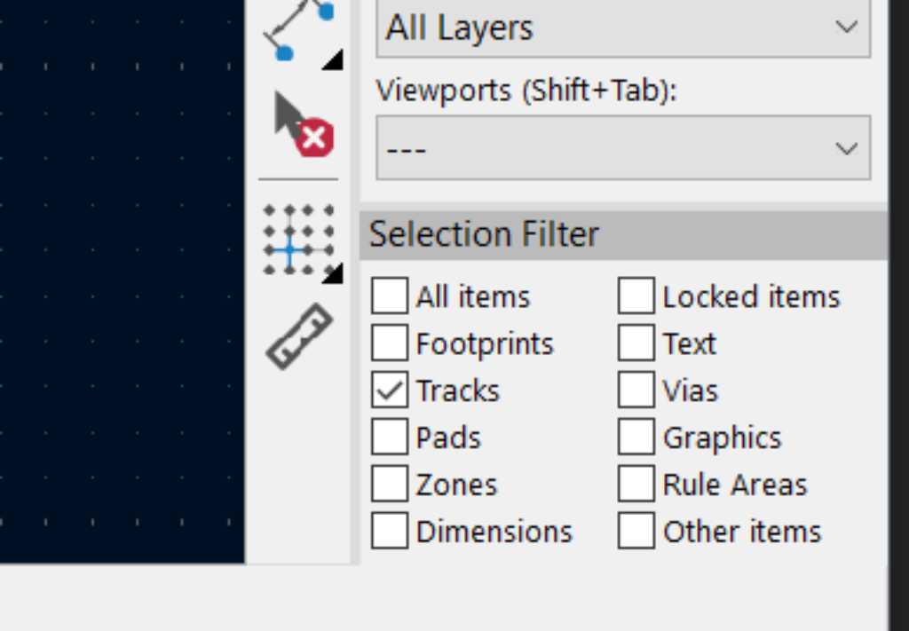
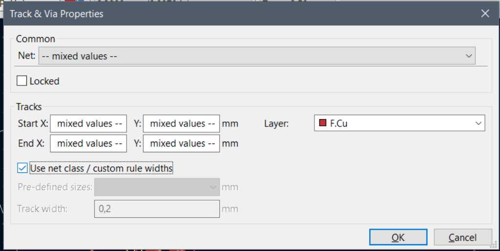
You should do this before you actually start drawing traces. Because otherwise you’ll have to change the tracks you already made. If you need to do this then set the selection filter to tracks, select all tracks and go to Properties (keyboard shortcut E). Make sure to check the “Use net class” checkbox and hit OK. This should change the width of all selected tracks:
Move components while keeping traces connected: use keyboard shortcut “D” (drag). As you can see it’ll show you when traces collide:
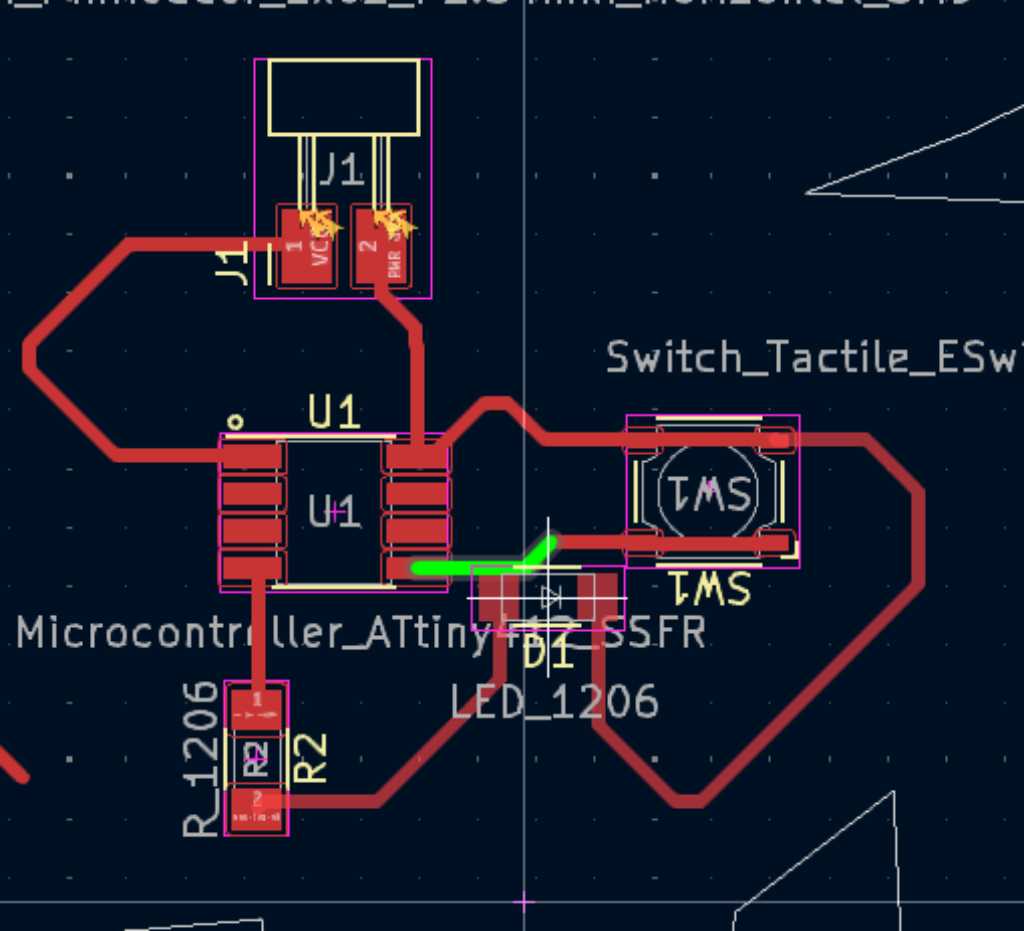
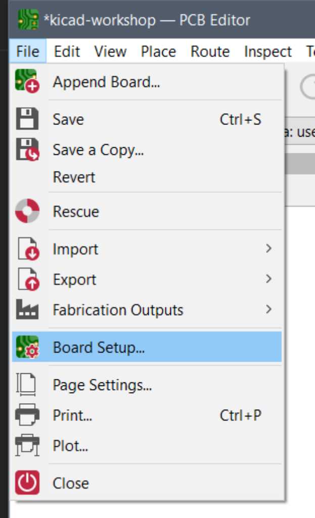
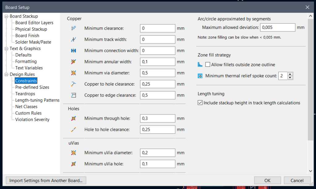
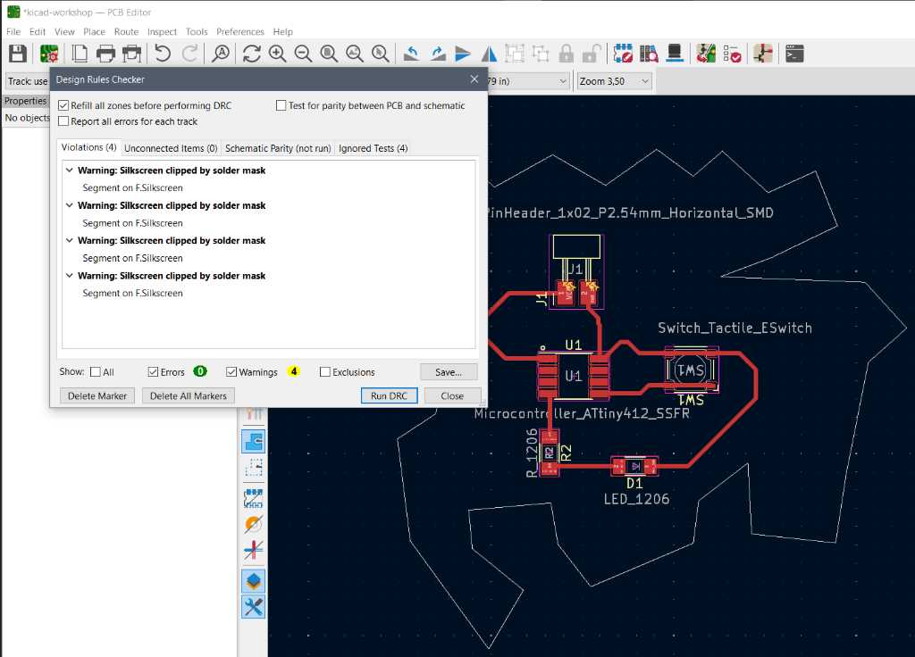
The design rule checks are setup in Board Setup:
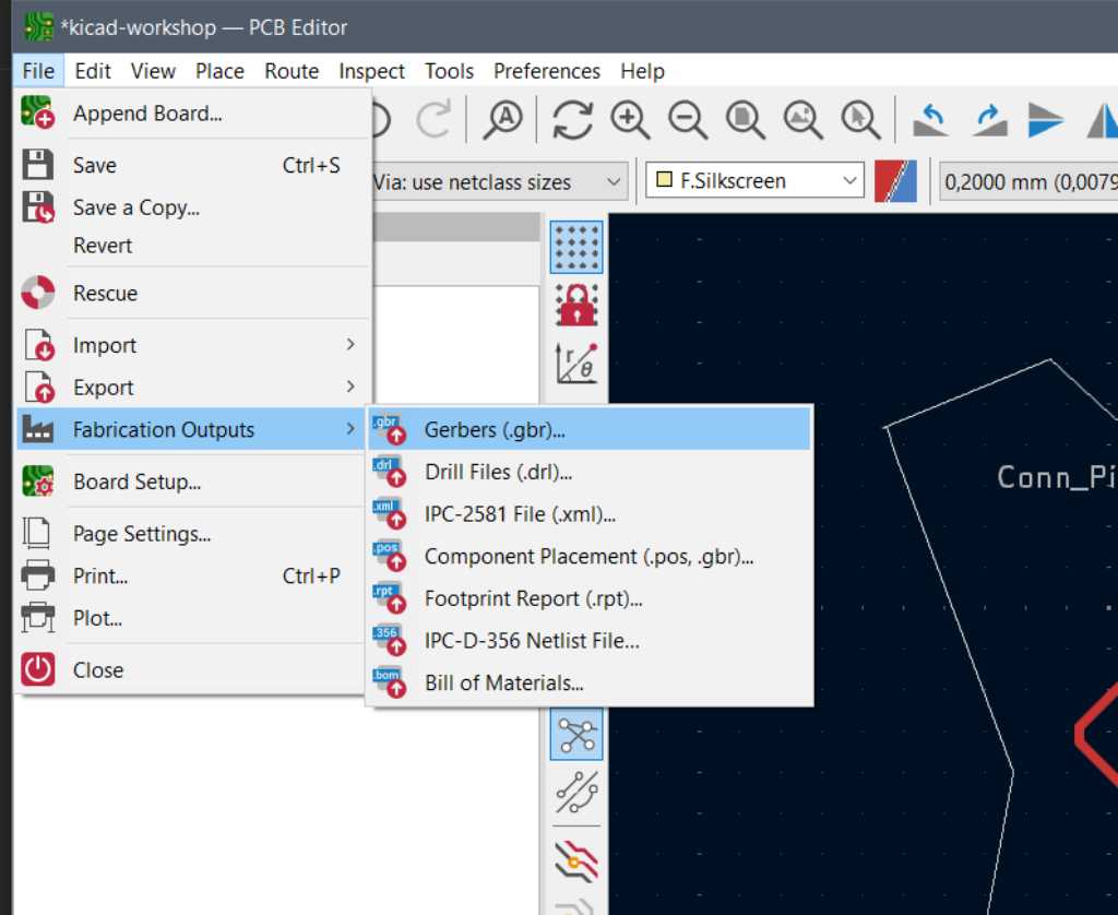
Create the fabrication files (Gerber files):
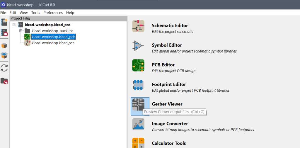
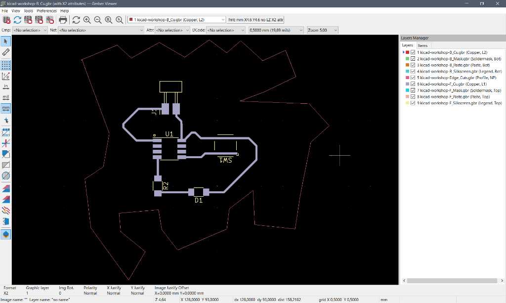
 Kicad has a Gerber viewer that allows you to check the gerber files you’ve created.
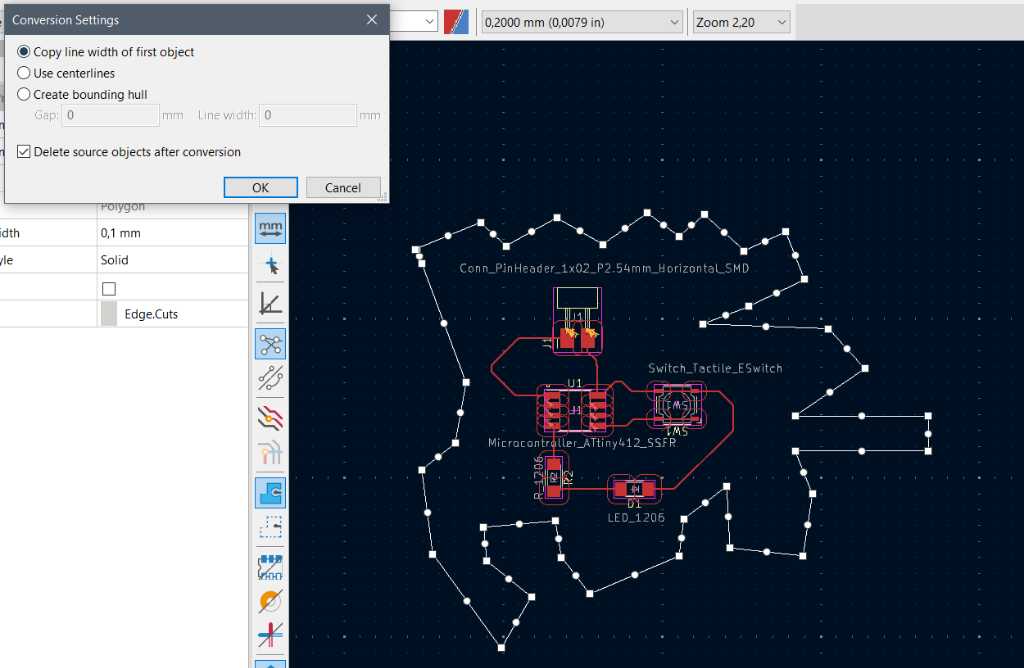
If you have a shape and need to add something to it you’ll have to convert the shape into lines:
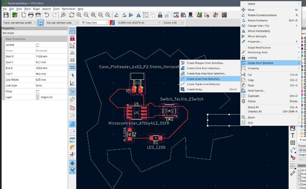 You can then break the lines and add anything you want to it. Next you select all these lines (note: use the selection filter set to Graphics) and create polygon from selection. Make sure to have “Copy line width of first object” selected:
Multimeter
The multimeter has no hidden secrets for me. I own a Fluke since before year 2000 :-)
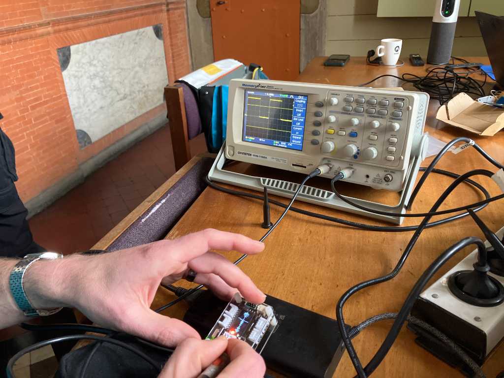
scope
Again, the scope has no hidden secrets for me either. No really, I searched the internet. There’s no easter egg in the gw instek gds-1152A scope. But here’s the PWM of Edwins Furby noise:
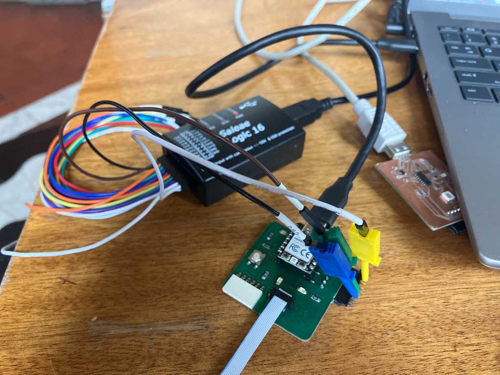
logic analyzer
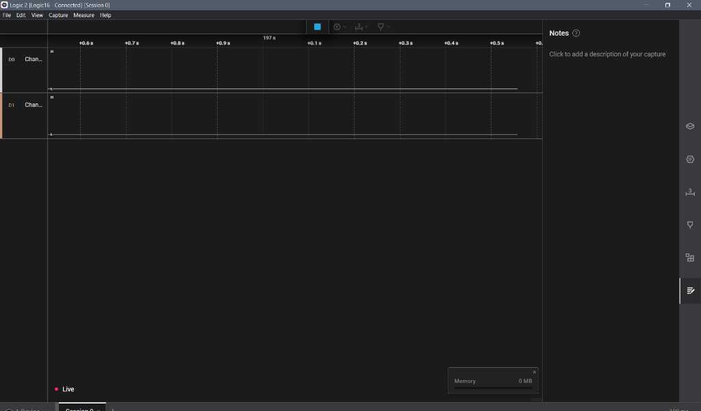
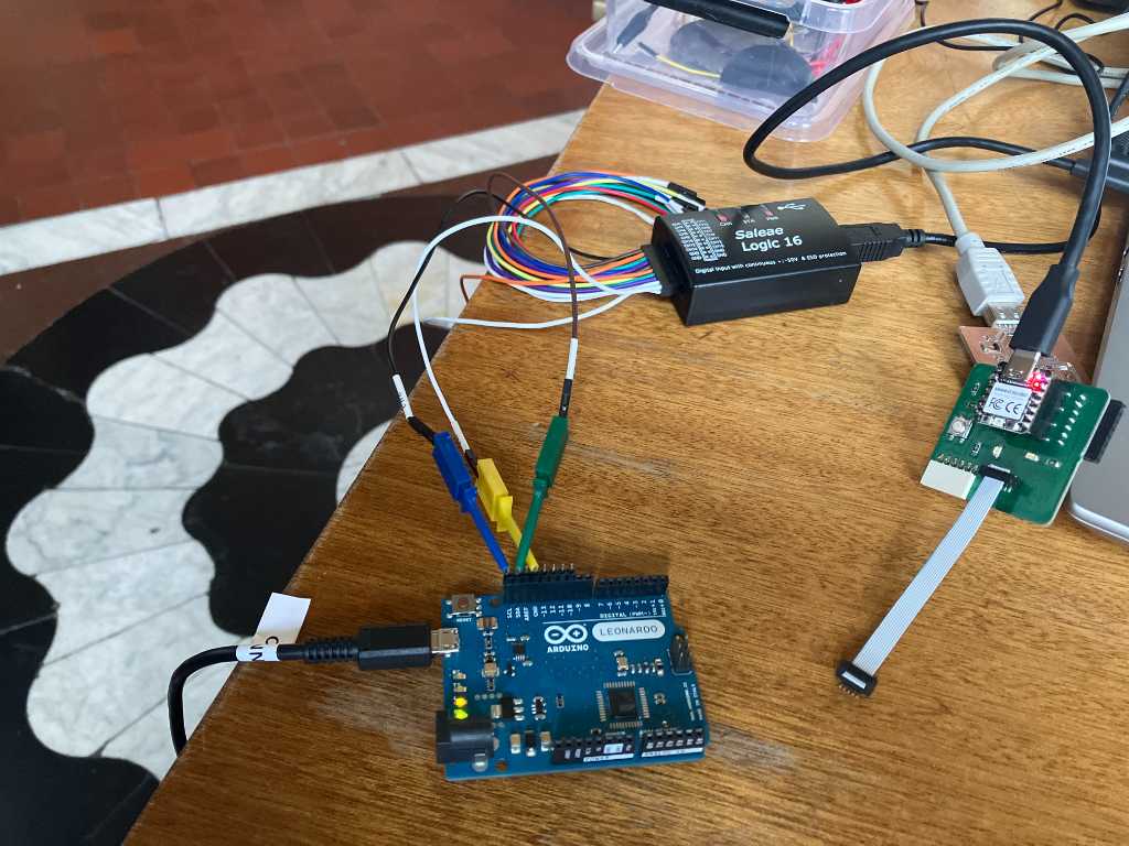
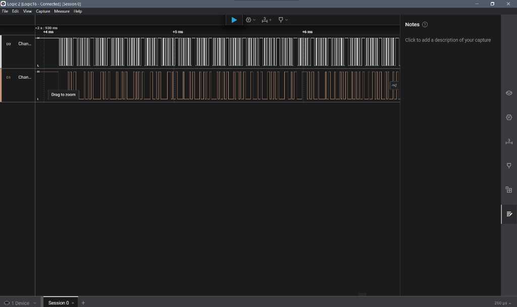
Here comes the important part of today: Checking with a logic analyzer why my Xiao RP2040 I2C address scanner of Embedded programming week didn’t work as expected. Here is it connected to the Saleae logic analyzer:
No response, not even a clock signal:
An I2C address scanner on a Arduino Leonard (on I2C hardware pins) does work:
So this means it’s a Xiao RP2040 PIO programming issue. I think the reason is that the pins aren’t defined correctly.
I’ve defined
#define PIN_SDA 9
#define PIN_SCL 10
based on D9 and D10 (from Quentorred):
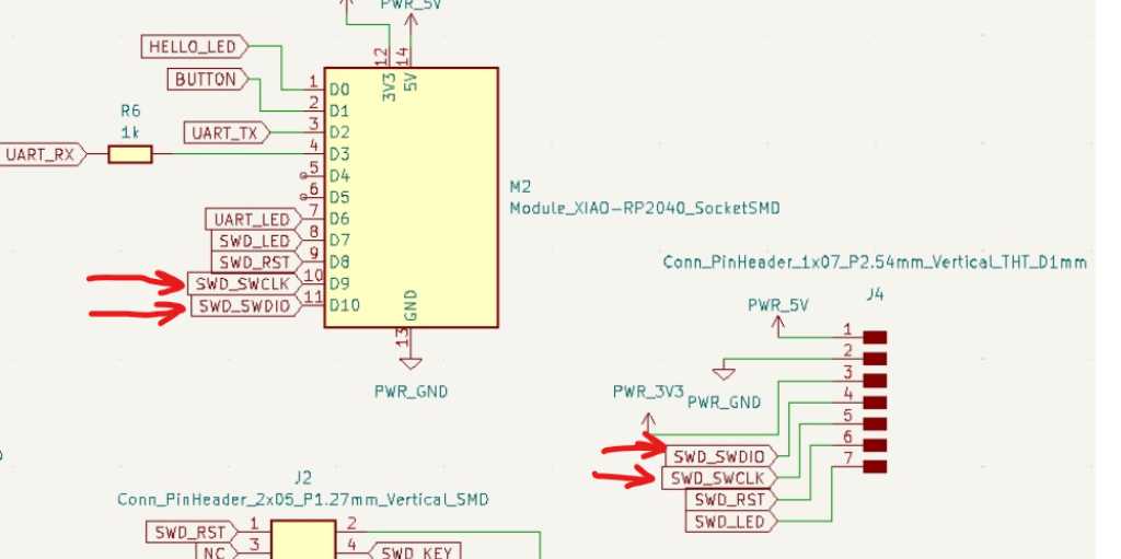
But I think in Arduino terms, these are actually different pins. Again according to quentorres documentation:
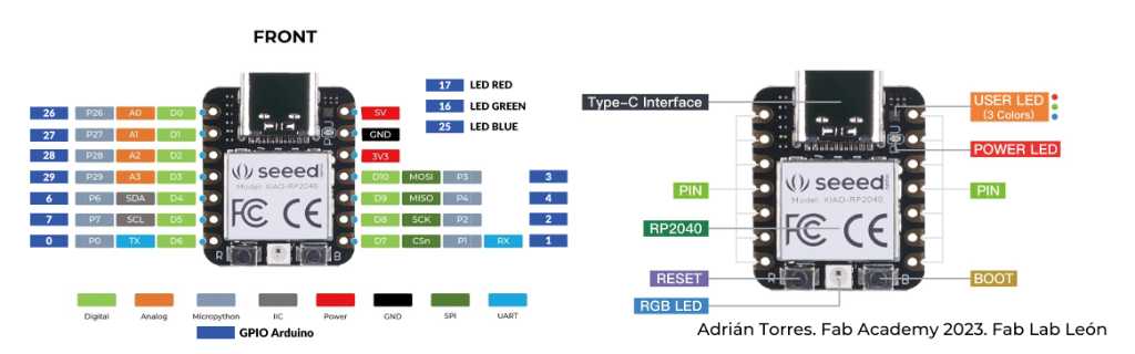
Note the dark blue pin numbers. These are the Arduino defined pins. So lets try:
#define PIN_SDA 4
#define PIN_SCL 3
But no, that didn’t do it either. So in discussion with Erwin, Henk and Edwin, we concluded that pin numbering must have been lost in translation. Defining a PIN_SDA to number 4 doesn’t mean it actually goes to pin 4 and if it does, it doesn’t mean that Xiao RP2040 pin number 4 is addressed. So that means a big brick wall.
Individual assignment
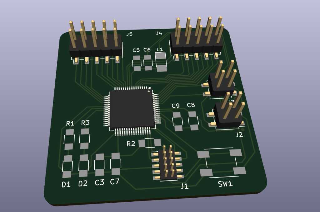
SAMD11C14 development board
I’ve never designed anything in Kicad before doing Fabacademy.
In Embedded Programming week I did my first design (SAMD11C14 based board) and that was actually pretty straightforward. So good vibes. I only used the fabulous Fab Electronics Library for KiCad for this design. I used the documention of Quentin Bolsee’s SAMD11C Devkit and the documentation of Adrian Torres.
Installation of Kicad and this library is explained in my documentation of bootcamp week.
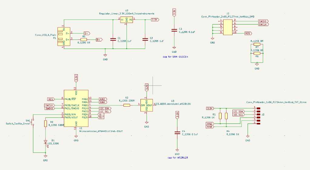
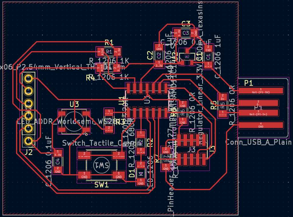
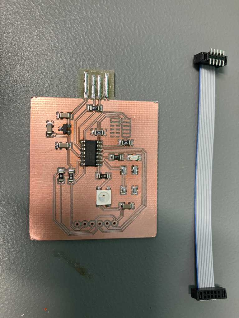
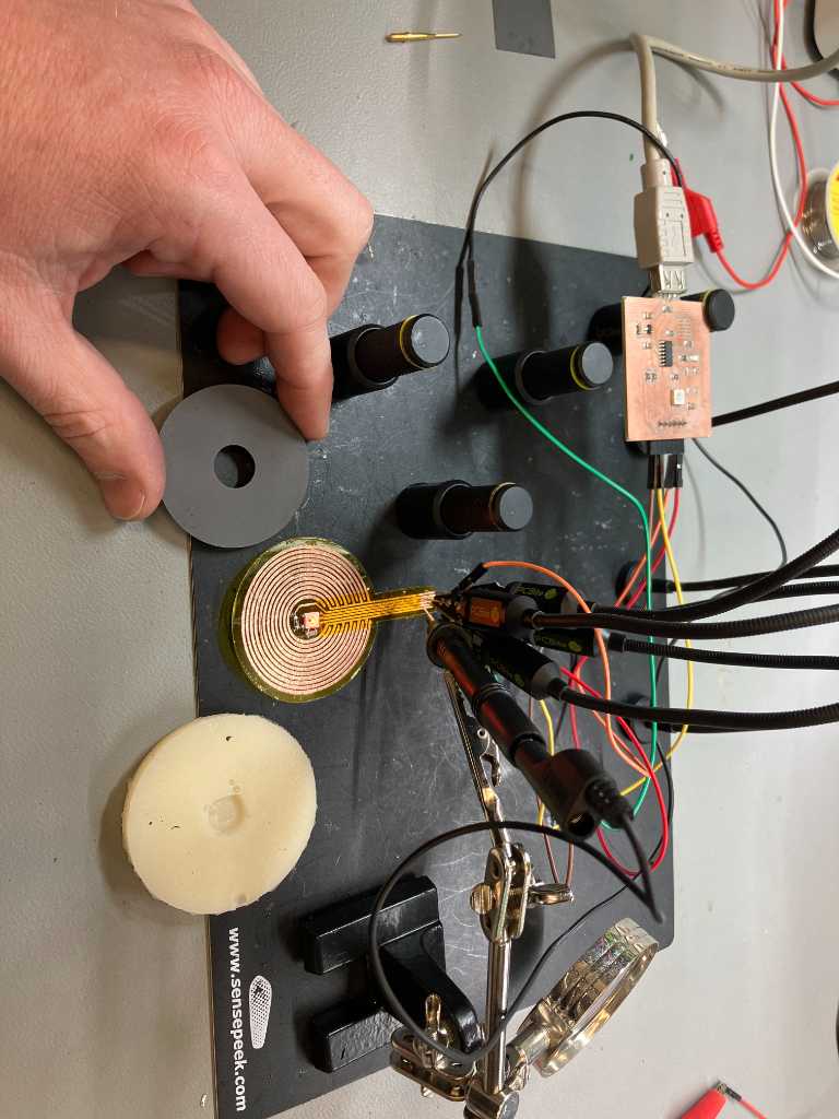
I used this board this week to test my self-made pressure sensor (for my final project):
This week I want to use Kicad more, creating custom footprints, a flexible PCB and a more complicated PCBs for my final project.
Custom symbol and footprint in Kicad
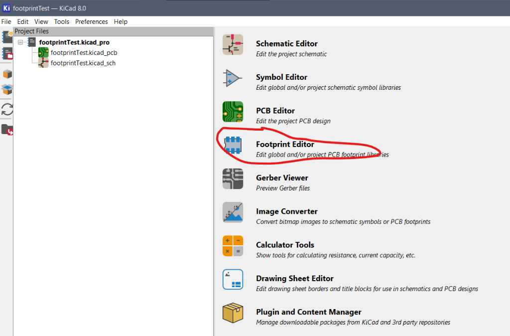
I created a test project in Kicad 8.0. Next I checked the Footprint editor to find out the easiest way to import something from Fusion into Kicad as a footprint.
The way of working is to first create a footprint, then create a symbol and then marry them so both the schematic editor as well as the PCB editor know that these two belong together. I found that this order is the easiest.
Create a footprint
The footprint editor:
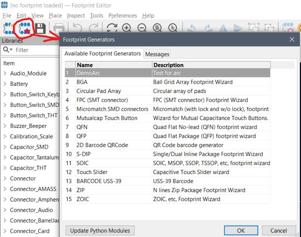
You can start drawing your footprint immediately, but there’s also a wizard. The wizard is basically a set of Python scripts with a few parameters that you can use to adjust the design.
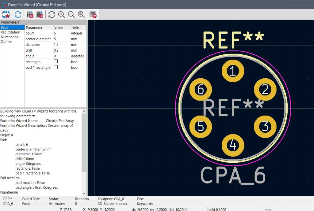
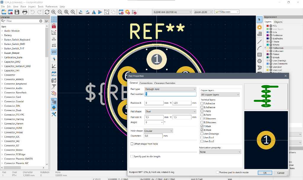
When you’re happy with your wizard output, just hit the “Export footprint to Editor” button and it is transferred into the footprint editor. If you doubleclick a pad, you can customize it further.
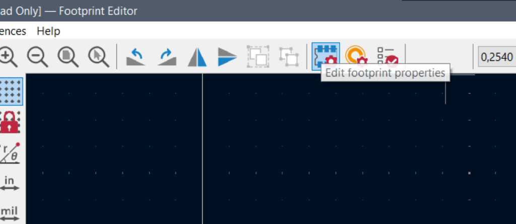
If you want to add the 3D model, click on the Edit Footprint Properties button and go to the 3D Models tab:
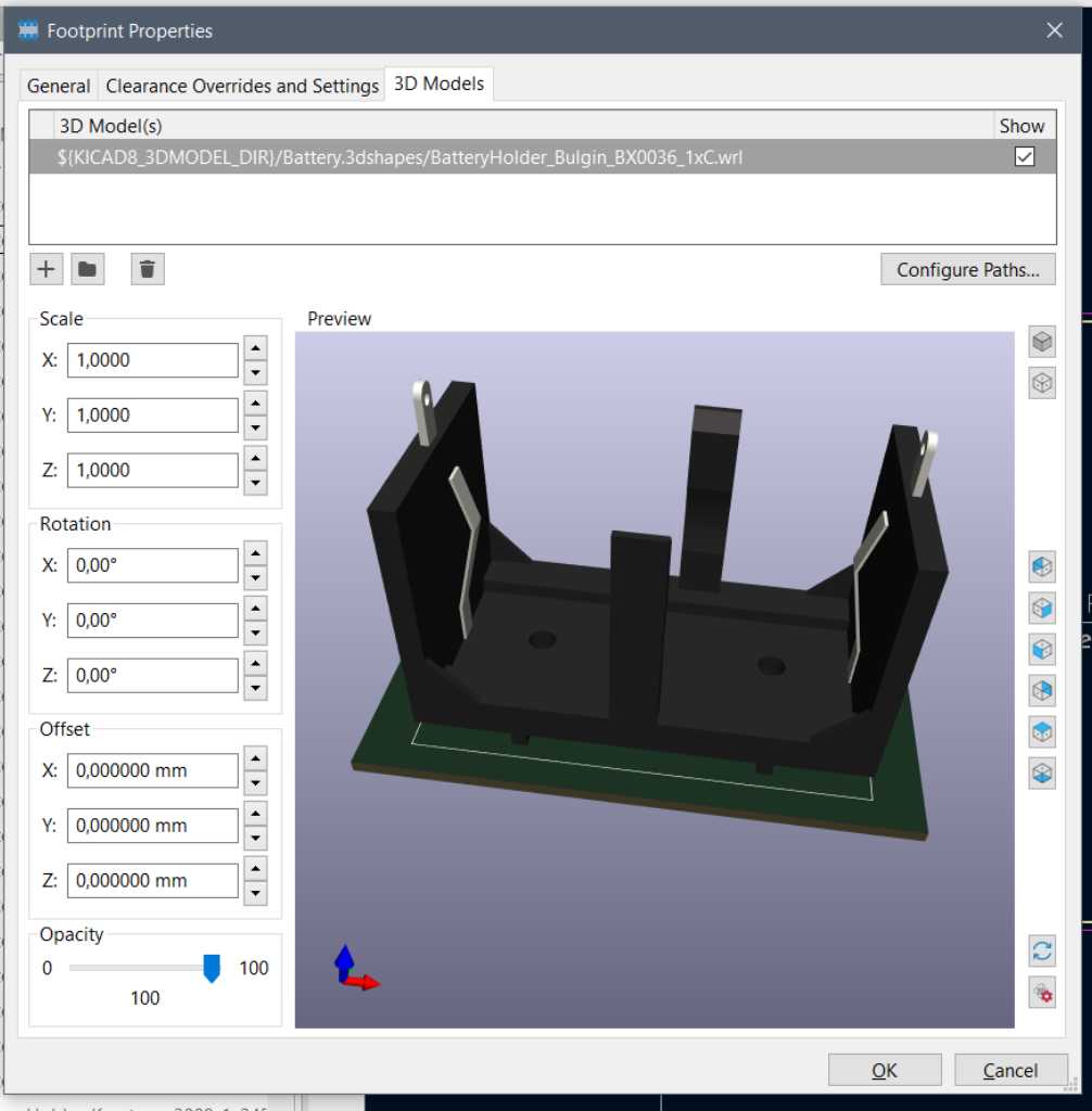
The 3D model should be a .step or a .wrl file. These are fundamentally different. According to the Kicad forum:
The two formats are fundamentally different. The wrl format is a tessellated surface mesh meant for making nice renderings (originally conceived for virtual reality) while step is meant to communicate parametric information between cad tools.
TLDR: use wrl to make pictures for your marketing guy, use step to exchange information with your fellow mechanical engineers.
WRL does not specify what its unit means. KiCad reads it as one wrl unit is equal to one inch for legacy reasons.
Save in a new library
I’m going to make a project specific footprint library.
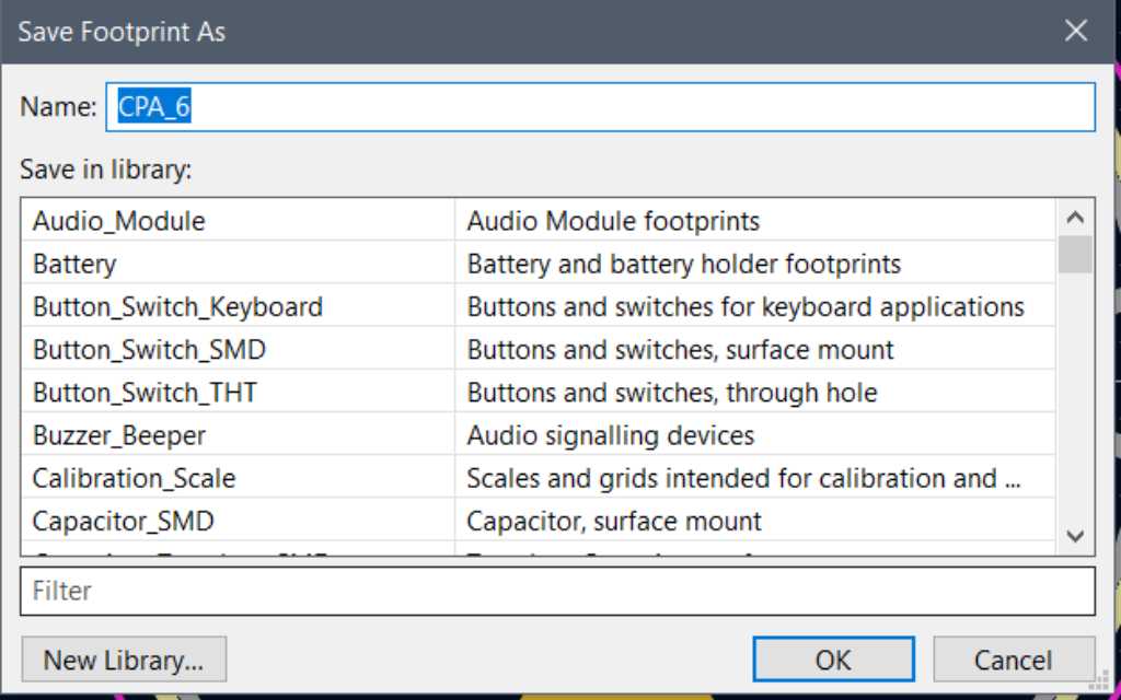
save library as a .pretty file. Select the newly created library:
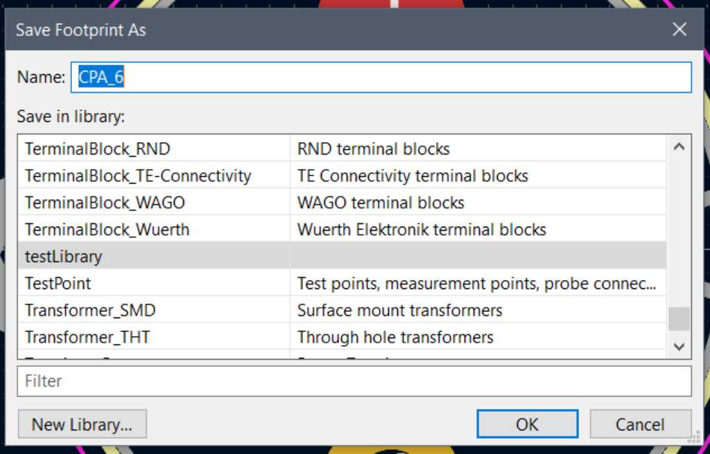
Give the footprint a name and click OK. The footprint is now saved in the selected library.
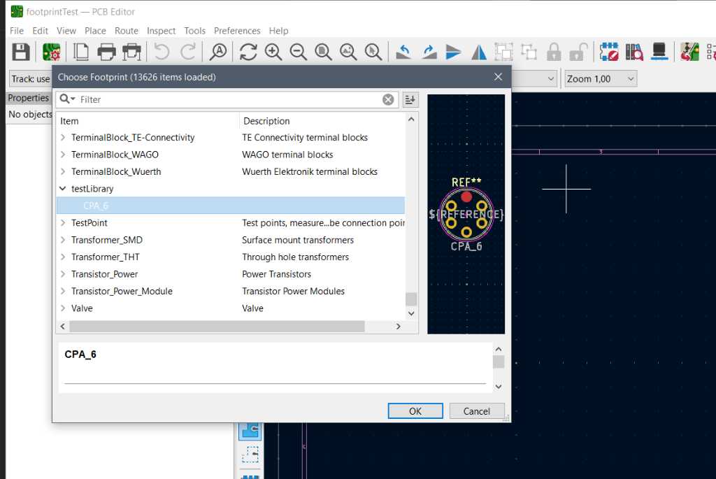
In the PCB editor you can now add a footprint and select the newly created footprint:
Create a symbol
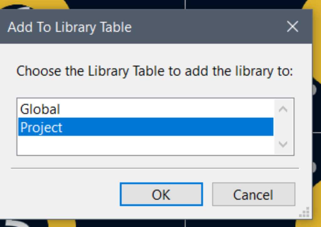
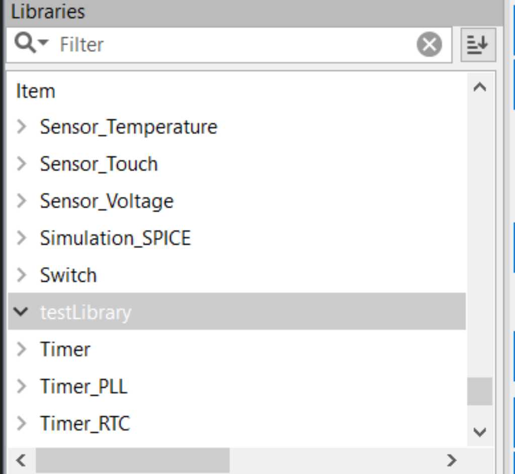
First select a library. If you want a project specific library then you have to create a new one:
Save it with an .kicad_sym extension.
Now the new library appears in the library section:
With this new library selected click the New Symbol button:
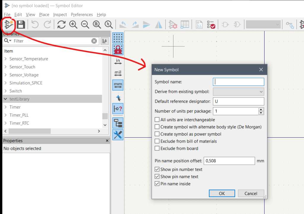
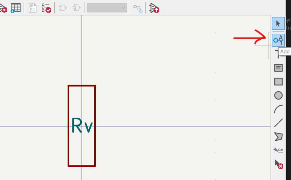
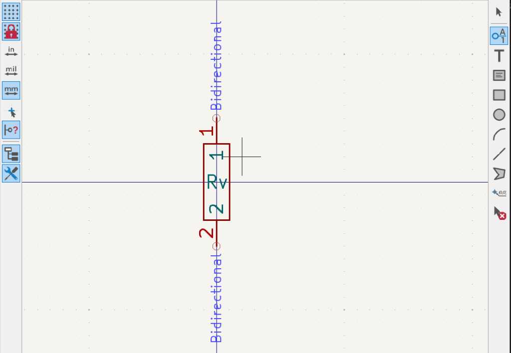
Give your symbol a name and click OK. Now you can draw your symbol and add pins to it:
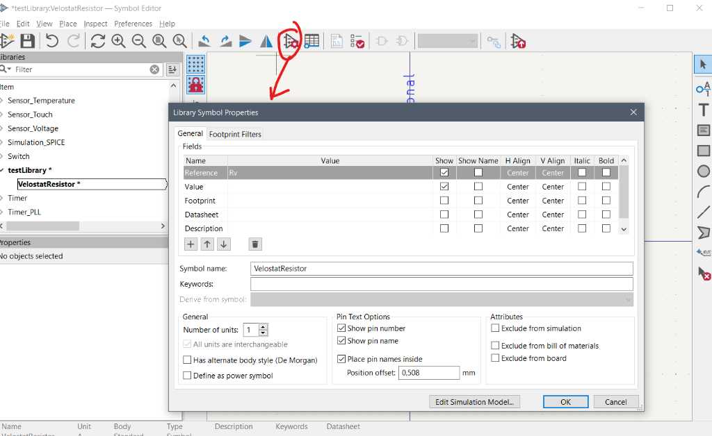
assign Footprint to symbol
While still in symbol editor, click the symbol Properties dialog to assign the previously created footprint to it:
test the new symbol/library
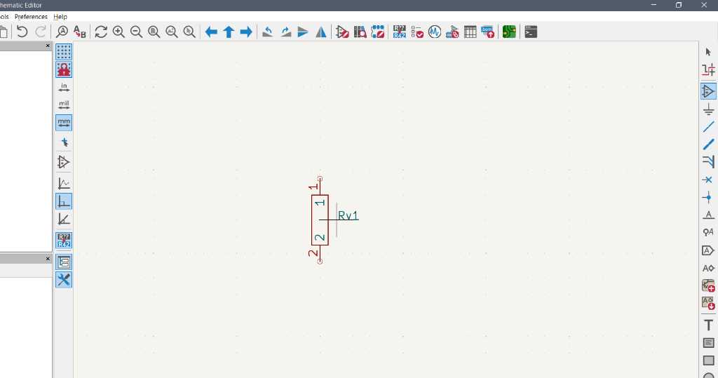
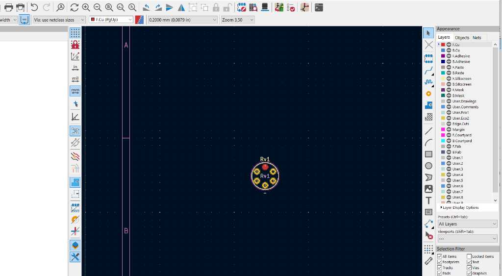
In schematic editor add a new symbol (keyboard shortcut A). Select the new component and check if both symbol as well as footprint appear:
On the schematic you’ll see this:
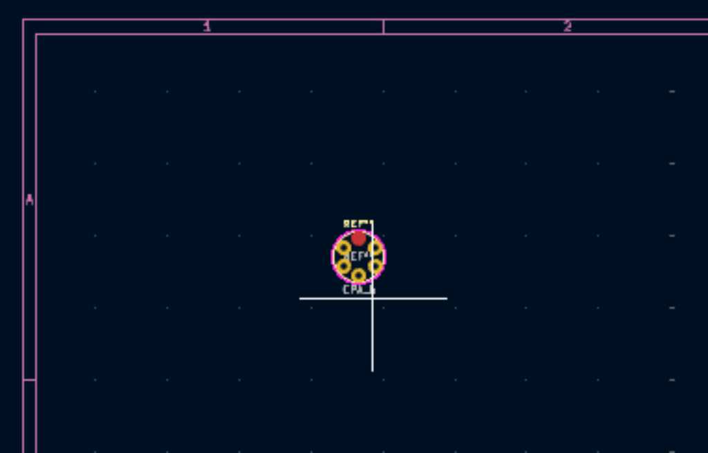
And in the PCB editor you’ll see this:
Flexible PCB
In the past weeks I already made 2 versions for my flex-PCB for my final project. These were based on cutting copper tape using our Cameo. I’m now going to make version 3. Goals:
- Custom footprint instead of custom traces (for better connection of traces to the footprint)
- Add an additional resistor for measuring velostat (instead of having this resistor on the microcontroller board)
- add a standardized connector so my sensor can be easily wired (FPC? IDC?)
- add a stiffener where the connector will be placed so it can be fixated using screws
Sending the Flexible PCB to a board house
For reference: a flexible PCB is also known as FPC. A Flexible Printed Circuit.
I want to send my flex PCB design to Eurocircuits as they are a preferred supplier of our university. That’s why I’ve read their design guides on mechanical layer, copper layers, carbon contacts to make the PCB according to their specs. By the way, they have an excellent description on setting up the design rules for Kicad.
Eurocircuits prefer the native CAD-formats as they can read these directly into the CAM-system without the need to output the data from the CAD-system into an intermediate format such as Gerber, meaning no interpolation issues with data output.
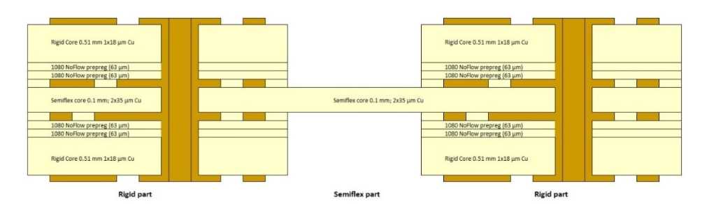
Eurocircuits doesn’t offer a standard flexible PCB. Instead they have semi-flex boards. Not with polyamide as core, but a thin layer of FR4 (100 micron) and specially treated copper (35 micron on both sides) that won’t break when flexing. At least not within 5 times 180 degrees at a 5 mm radius. The big pro of this is that it is much cheaper than polyamide-core flexible PCBs.
Also I like to use carbon contacts because this is used in commercial products with velocity sensing pads. Eurocircuits can make this:
carbon contacts -> eurocircuits design guide
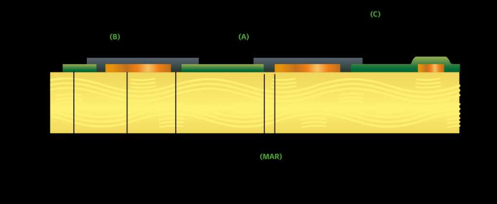 Minimum carbon to carbon spacing (A): 0.400mm (16mil)
Minimum carbon line width: 0.300mm (12mil)
Minimum carbon on copper overlap (B): 0.200mm (8mil)
Minimum carbon on Soldermask overlap (C): 0.100mm (4mil)
These rules mean that you must have a minimal isolation or spacing of 0.800mm (16mil) between the copper elements of a typical carbon finger contact.
I checked their calculated costs for 100 pieces of 100x50mm semi-flex PCB:
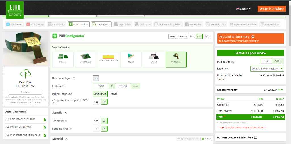
So that is almost 2000 euro, or 20 euro per piece.
If I want to have carbon ink on top, they can’t use their pooling service. So that means:
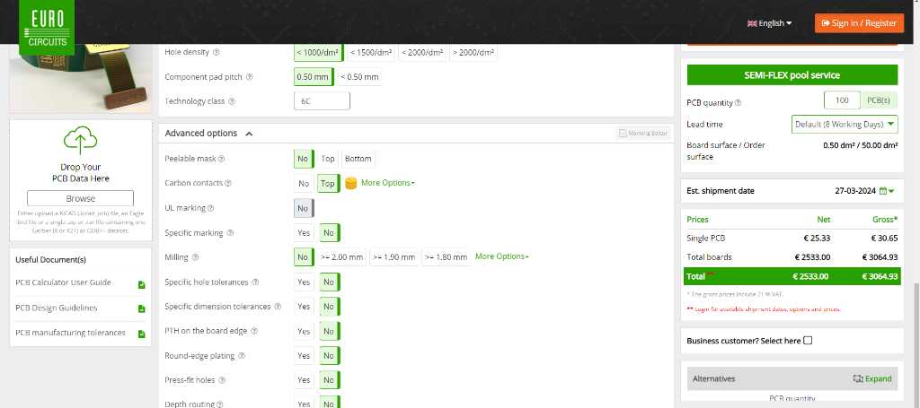
3065 euro, or 30,65 euro per piece. Auch, waaaayyyy over my budget.
So checking JLCPCB:
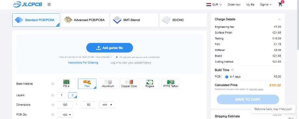
120 euros for 100 pieces including shipping. 1,20 euro per piece. That’s more like it.
I checked PCBway as well and that would end up to 370 euro including shipping, so 3,70 euro per piece. Clear win for JLCPCB in terms of price.
Unfortunately both JLCPCB and PCBway don’t offer carbon contacts. As said, commercial products with velocity sensitive pads use either gold plated pads or carbon ink covered pads. I found a good explanation of it at reddit:
The black layer is a conductive carbon loaded coating used to make a reliable switching contact with the (also carbon loaded) plastic bit.
For gold to be reliable it needs to be thicker then the flash used in ENIG plating, so the gold plate is expensive in quantity where the carbon ink adds far less cost in production volumes and is actually quite reliable. Choice probably depends on which fab you are using.
…
The benefits of using the Carbon Contacts mostly lie in the fact that the carbon has an extremely high surface area, so when it Contacts the pad it will make a good connection with very low amounts of bouncing. They are also more stable than bare metal Contacts in a lot of cases, as the Carbon doesn’t rust or tarnish, while copper for example tarnishes quite quickly.
According to Eurocircuit documentation:
Electroless gold (ENIG) gives excellent solderability, but the chemical deposition process means that it is too soft and too thin to withstand repeated abrasion. Electroplated gold (hard gold) is thicker and harder making it ideal for edge-connector contacts for PCBs which will be repeatedly plugged in and removed.
It seems cheaper commercial products don’t use gold plating because it has to be thicker and thus more expensive at high quantity production. But carbon contacts is very expensive in low quantities. So I’ll decide to do ENIG god plating, just for cost. It’s a prototype after all.
Design
So I’m not going to design my flexible PCB with a carbon layer. It’ll get an ENIG (Electroless Nickel Immersion Gold) surface finish. This is a nickel and gold layer. The gold layer by default is 1 micro-inch, meaning 0,0254 micrometer but JLCPCB offers 2 micro-inch as well. Price uplift isn’t that much, so that sounds like a plan.
JLCPCBs design rules for FPC can be found here. The minimum trace widths and spacing is much smaller than what I made to be used on the Cameo. So no worries that they can’t make this.
To check for these design rules in my Kicad project, I used the custom design rules located at this github page.
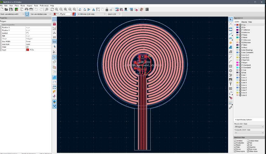
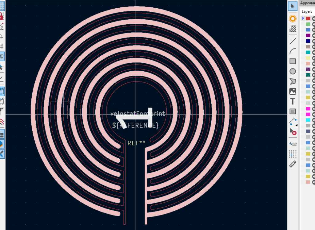
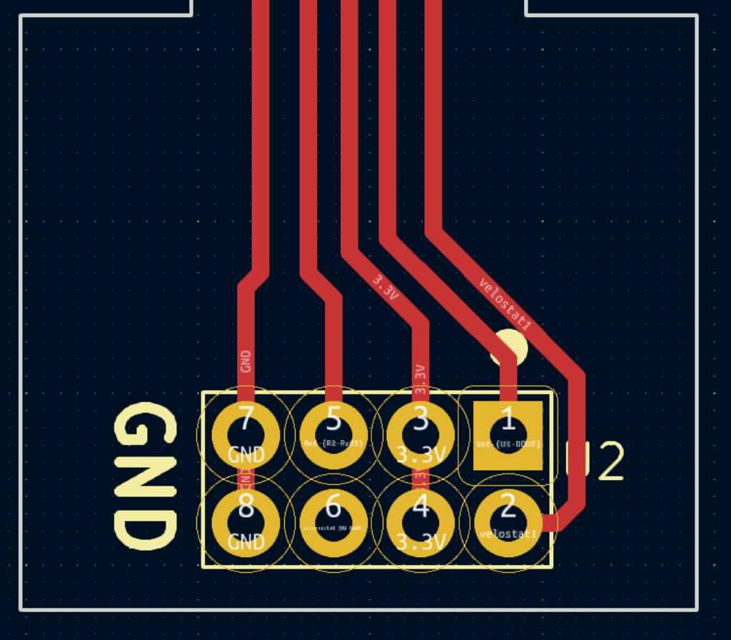
Let’s first make a custom footprint for the velostat circles, using my notes above.
As documented on my final project pages, I already made this (part that needs to become a custom footprint is selected):
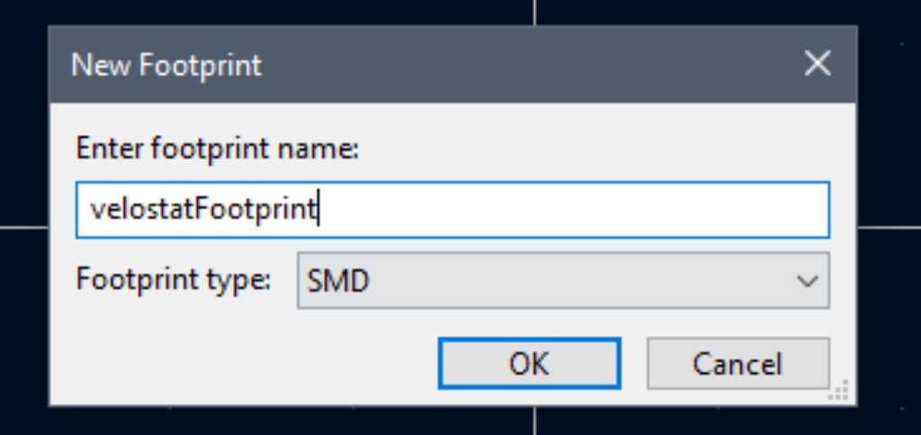
I created a new library and with that library selected, I added a new footprint:
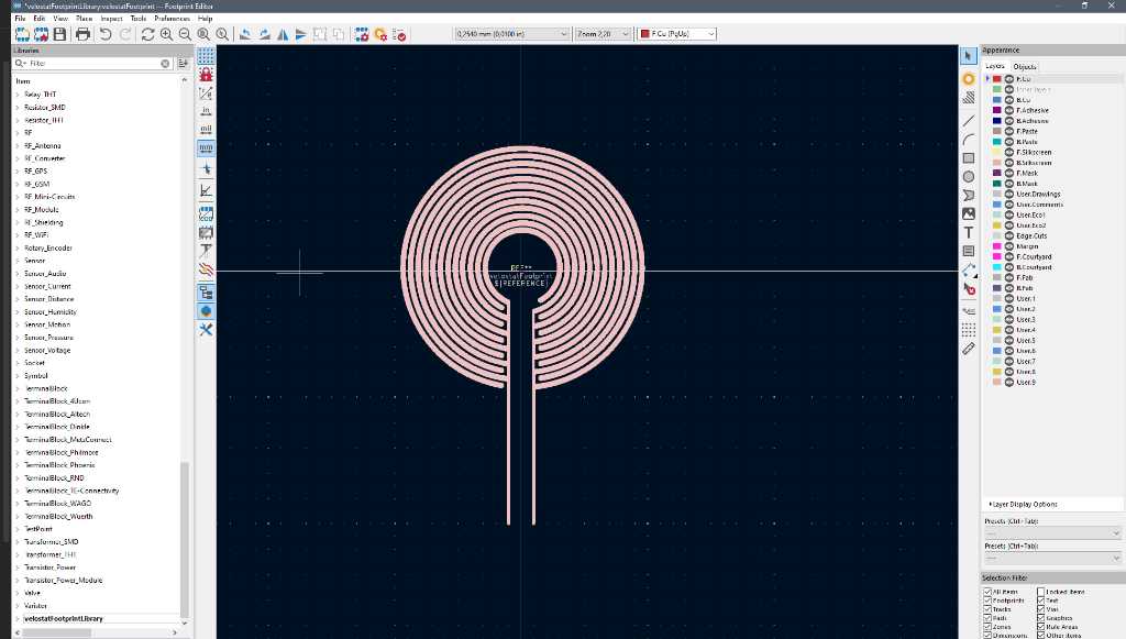
Now I can copy these traces and pasted them in this footprint:
Next is to make sure that these traces are identified as pads. The way to do that is:
add a new pad (Place - add Pad)
right-click and select Edit Pad as Graphic Shapes (CTRL-E)
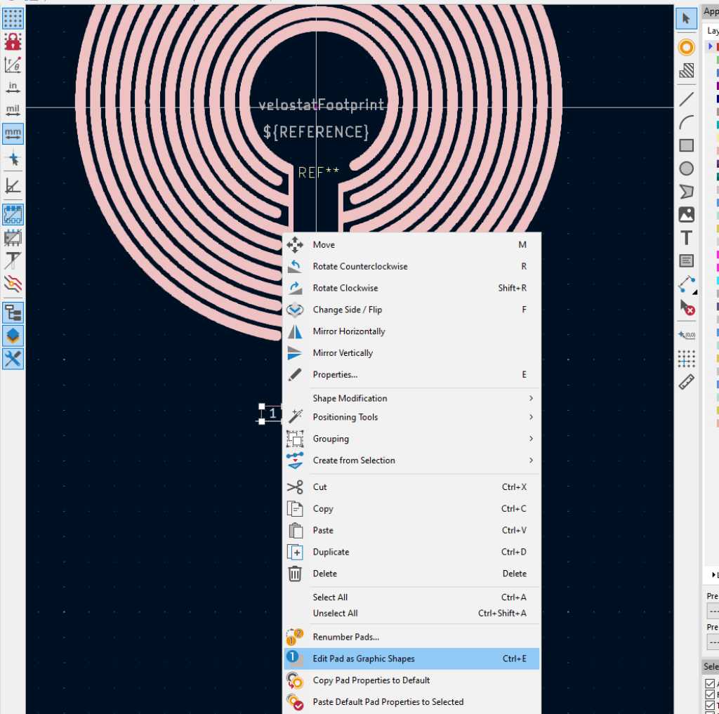
Make sure the pad touches or overlaps the trace
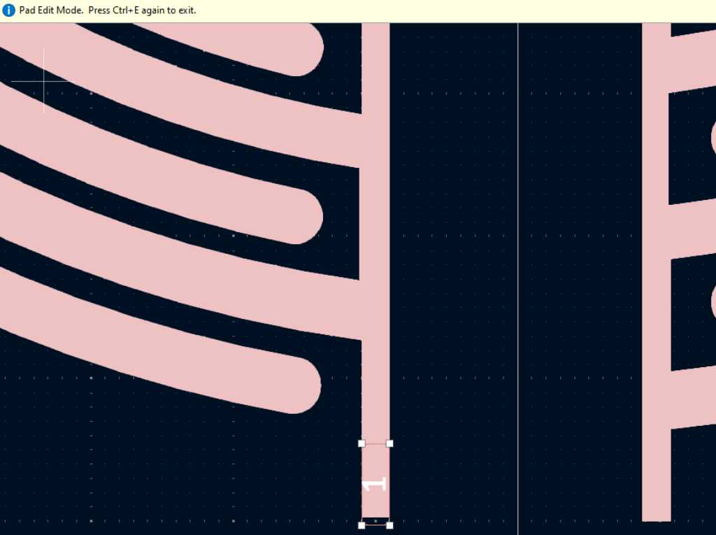
press CTRL-E to exit edit mode. Now the full trace became the pad.
The point where this pad was added will be the “snapping” point. Any track will snap to this specific point. Maybe you don’t want that. If so, you can hold shift while making the track and it will happily connect to another area of the pad.
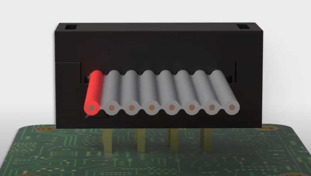
The pressure sensor will have to be cables to the microcontroller PCB and from one to the other. I searched for a cheap and easy way to get this done. Here’s what I think will work:
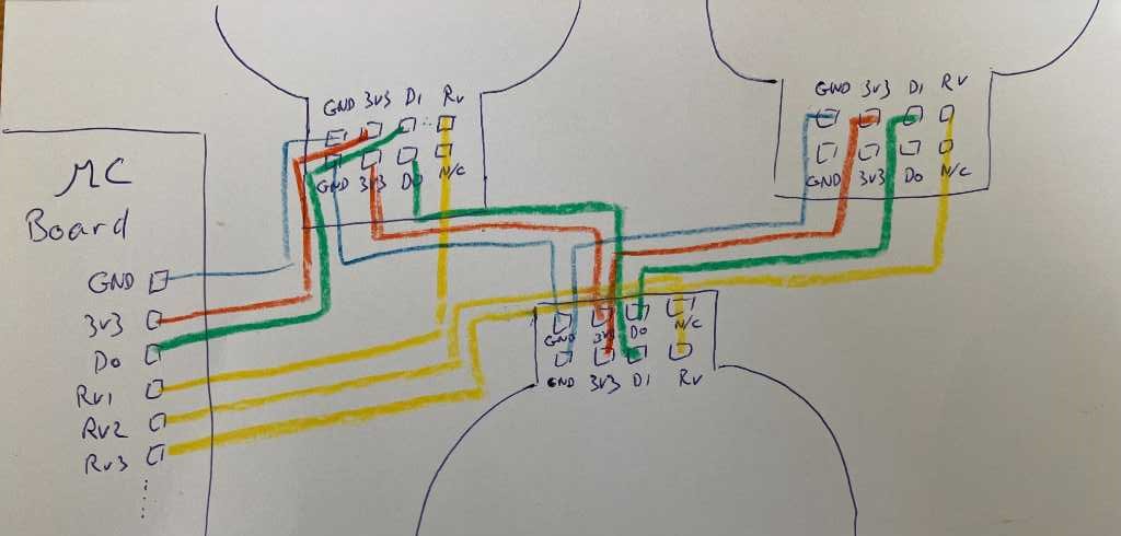
So I can make a cable assembly and go from one sensor to the other with power, ground, and WS2812B data. The sensor output voltage RV1, RV2, etc go back to the microcontroller board.
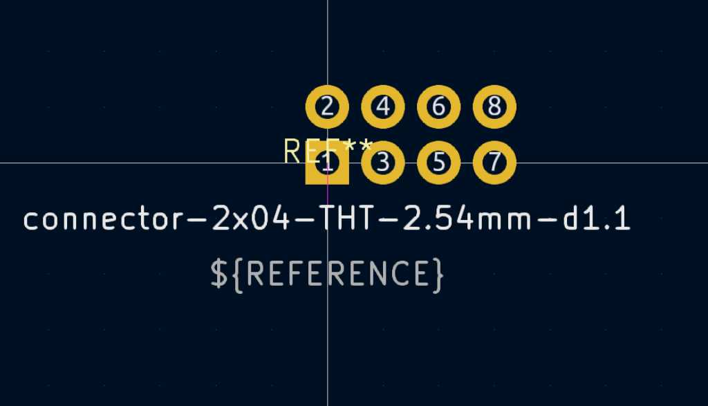
The cheapest way is to use ribbon cable. A suitable and cheap connector is this direct-wire-to-board connector: digikey part number 2987-CA2308PA10Z-ND which costs 28 eurocents a piece. It works with standard 1.27mm flat ribbon cable. (images from the manufacturer).
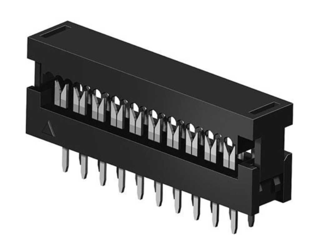
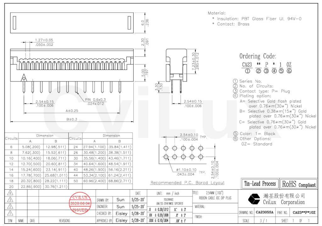
the size of this connector is (LxWxH) 7.62x6x7.3mm. And it uses a standard 2.54mm pitch through-hole PCB board layout with 1.10mm drill holes.
For this I need a footprint and a symbol. So let’s make it:
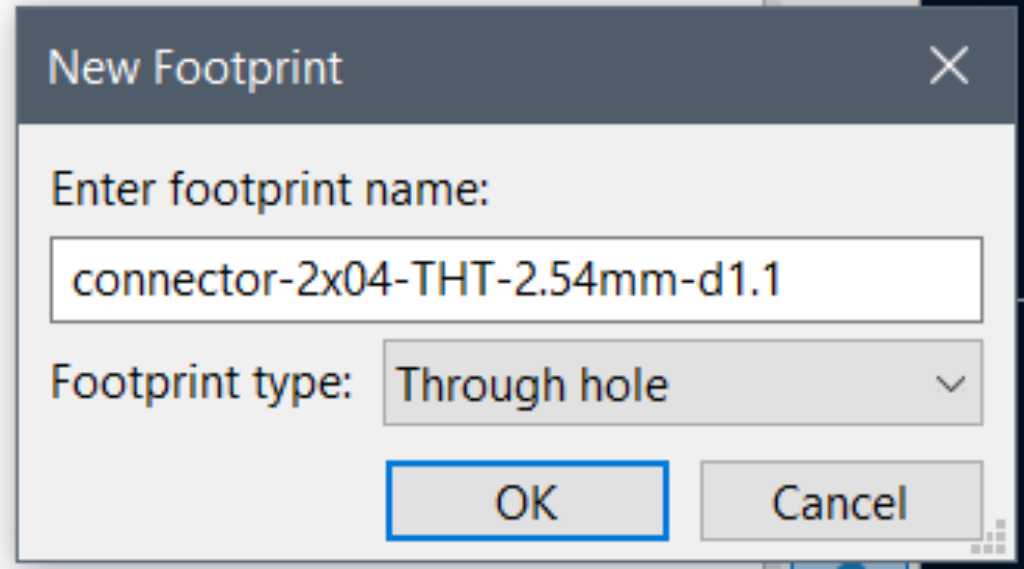
I set up the default pad properties for the Add Pad Tool as such:
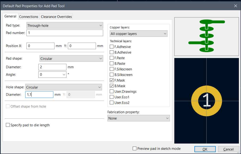
The hole size is given by the manufacturer of the connector. The pad size is not. So this post on the kicad forum notes that the pad should be at least 1.8 times the diameter of the hole, or at least 0.5mm larger. In my case resulting to a 2.0mm pad size.
And I also created the accompanying symbol:
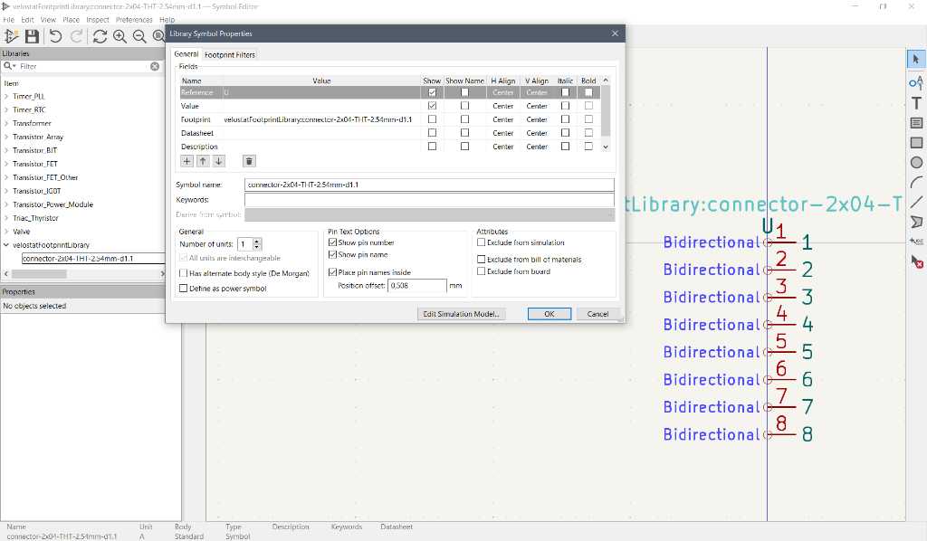
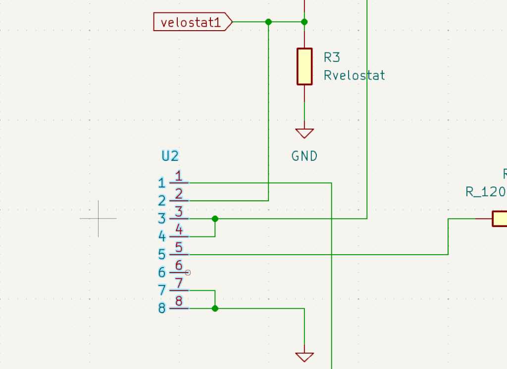
And adding it to the schematic and to the PCB design:
I’ve also added a stiffener to the flex PCB at the location where the connector and the mounting holes will be. I chose 1.6mm FR4 as stiffener so this part will be similar in thickness as a “normal” PCB.
The length of the smaller part between the circle and the connector part will depend on my mechanical design. Here’s a screenshot of the flexPCB as drawn in Fusion, with measurements that fit the mechanical design of the sensorfixture:
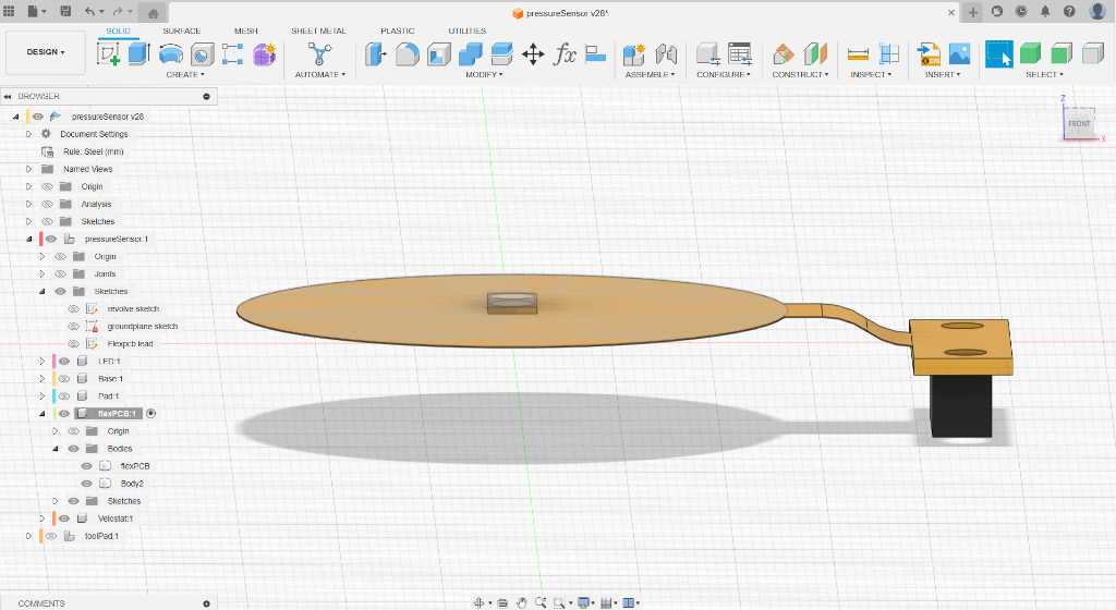
Measuring from fusion, this small part should be 3.89 + 4.88 + 4.88 = 13.65mm. I’ll make it a bit larger (15mm) because I have space to make it larger and having it too short is bad.
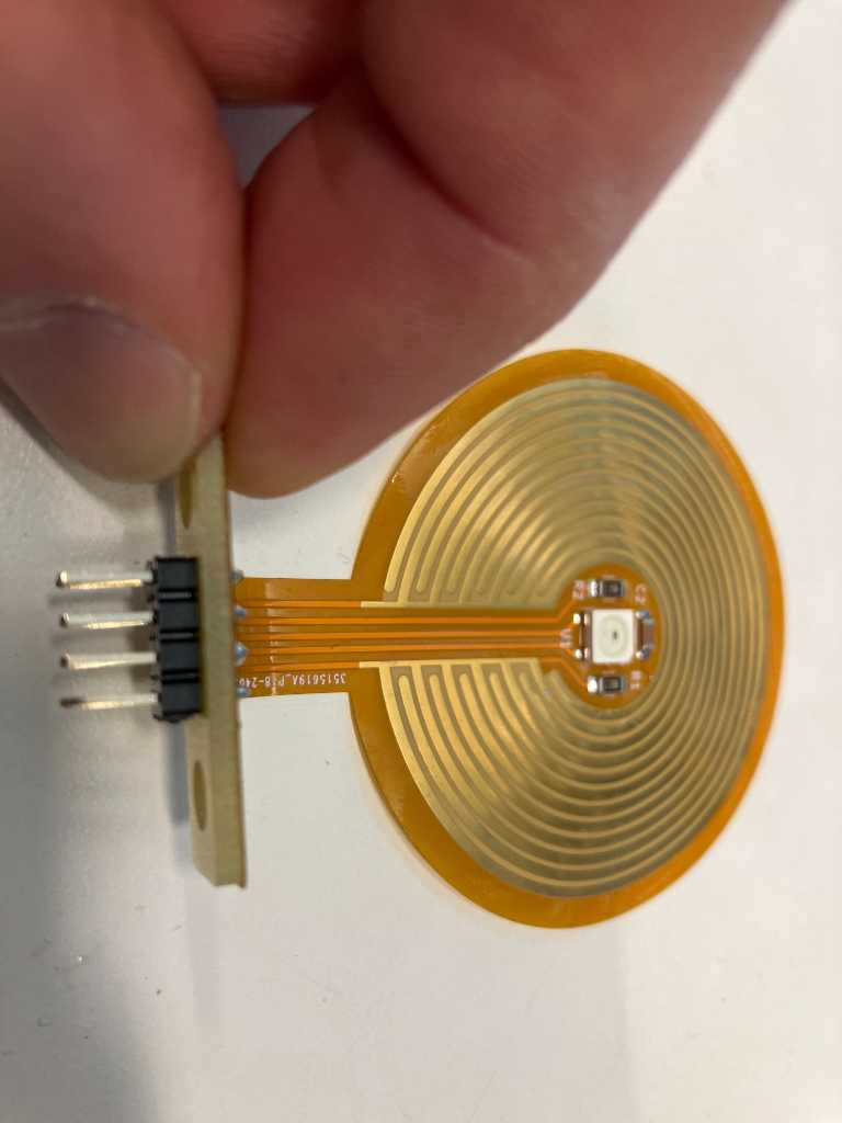
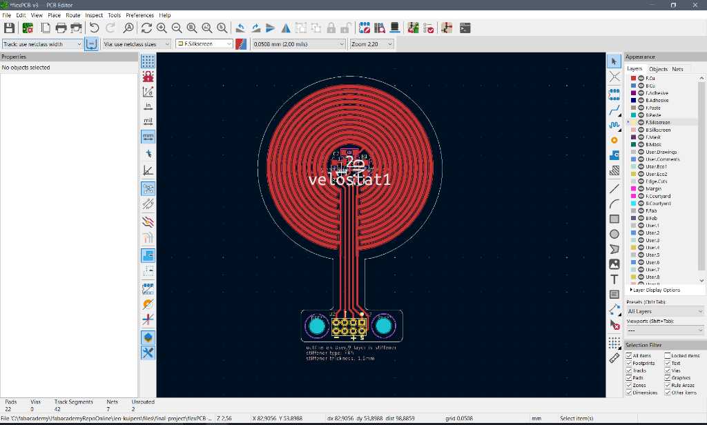
The end result:
To export this design into Gerber files that are suitable for JLCPCB, I’ve used their tutorial. After exporting the gerber and drill files, I confirmed these files using the Kicad Gerber Viewer:
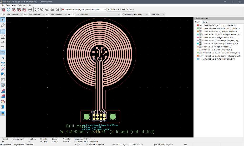
Done. Zip it, and send of to the PCB house!
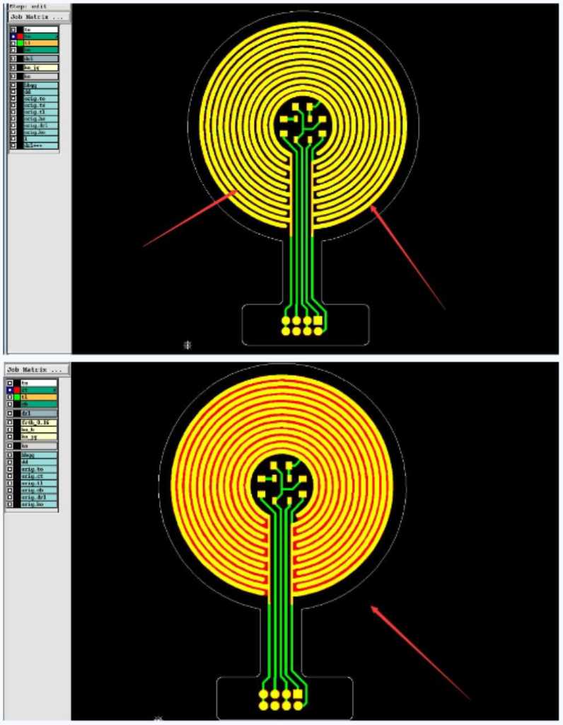
The JLCPCB gerber previewer shows my design like this:
And that’s how I want it. It’ll be around 150 euros for 100 pieces with these settings:
- 1 layer
- 0.11mm thickness
- yellow overlay
- white silkscreen
- 2 U” gold thickness (ENIG)
- 1 oz copper thickness (equals to 35 um)
- FR4 stiffener of 1.6mm thickness
I tried to panelize the flex PCBs to see if that’s cheaper. I could fit 24 on one sheet. That would cost around 170 euros so that’s not cheaper.
So this one is going to be send to the PCB house. Fingers crossed things will work out well!
There was only one issue that the PCB house came back with. Instead of soldermask, it is common to use a coverlay to protect the circuitery. This is because soldermask isn’t flexible and so it will break when flexed. A coverlay serves as a solder resist for flexible PCBs and is made out of polyimide with a epoxy or acrylic based flexible adhesive. But processing it is entirely different. It can’t be etched so holes and shapes need to be lasercut, drilledrouted or punched. That means there are some different design guidelines. In my design, it wasn’t possible to add coverlay in between the round traces. This area was too small and too long. So instead, they advised to don’t apply coverlay on this section at all. This sounds fine to me.
After a while I received the flex PCBs. They look awesome! And they actually work :-)
Here’s a soldered version. More info in the pressure sensor section of my final project.
Final project module board PCB
My final project PCB will be based on a SAMD21J18. Documentation of this can be found in the final project section. I measured the space I have for the board: It’s 45x45mm.
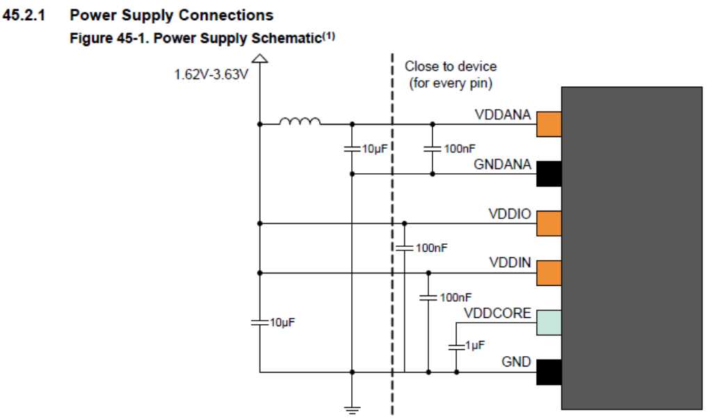
I’m going to use the recommended power supply design (filtering) as discussed in the SAMD21 datasheet:
The design is not fully done yet and I didn’t receive the components yet so I can’t test, but it’s almost done:
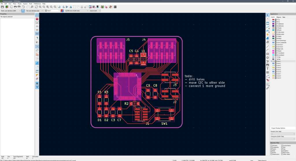
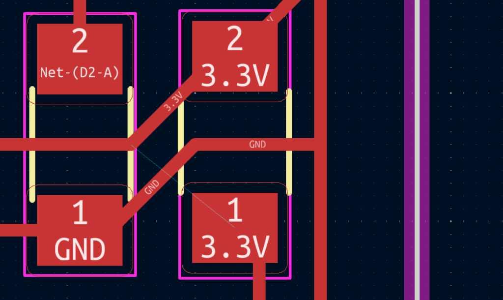
One thing I ran into is how to use a 0 ohm resistor as a bridge/jumper. The DRC keeps giving me errors that I didn’t connects the nets correctly:
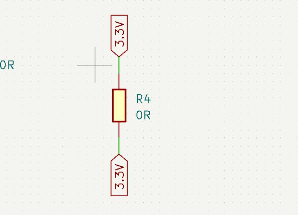
I don’t know how to solve this (yet?). But then Krisjanis Rijnieks comes to rescue!
He investigated the jumper issue and added a Jumper_1206 symbol to the fab library. He tested it and it works without error in ERC and DRC. And if you want to use any other 2-pin footprint instead a 1206, you can reassign it in the footprint assignment tool via schematic editor.
Link to repo
My SAMD11C14 PCB can be found in this repo: https://gitlab.fabcloud.org/academany/fabacademy/2024/labs/waag/students/leo-kuipers/-/tree/main/files/06_embedded-programming?ref_type=heads
The flexible PCB design can be found in my final project repo:
https://gitlab.fabcloud.org/academany/fabacademy/2024/labs/waag/students/leo-kuipers/-/tree/main/files/final-project/flexPCB-v3?ref_type=heads
The other stuff of this week can be found here: https://gitlab.fabcloud.org/academany/fabacademy/2024/labs/waag/students/leo-kuipers/-/tree/main/files/08_electronics-design?ref_type=heads
What I learned this week
Successes
Kicad is a major success. I highly enjoy working with it, it was much smoother than I thought.
Designing the flex-PCB was fun too. And got it to the fabhouse so again a big success for me.
Various
Electronic resources: Adafruit, ohmify, sparkfun, starting electronics, raspberrypi.org
More advanced electronic resources: Circuit Bread, Circuit Digest
Fusion
I’ve used Fusion in the past to create PCBs. It’s a fairly straightforward process. Lot’s of tutorials are available online. The major advantage is that PCB design is combined with 3D modelling and you’d keep everything in one software program. You can derive the PCB outline from your 3D model of the casing and they will stay in sync (change one will result in a change to the other).
Electronics design in Fusion replaced Autodesk Eagle. As there are many libraries available for Eagle, there is an easy way to use these libraries in Fusion.
Autodesk library.io is Autodesks way to provide library management and collaboration for Eagle. Shared libraries created in Eagle are stored here. It can also be accessed from Fusion so it can act as a bridge between Eagle an Fusion electronics libraries.
Next to this there are various online resources that provide libraries that can be used. Some of them have plugins for Fusion to make importing easier:
- Ultra librarian: has plugin for Fusion. Signing up for a free account is required.
- SnapEDA: has plugin for Fusion.