electronics production
Topic(s) of this week
- electronics production (video, review)
- Described the process of tool-path generation, milling, stuffing, de-bugging and programming
- Demonstrate correct workflows and identify areas for improvement if required
Hero shots
Assignments
Group assignment
- Characterize the design rules for your in-house PCB production process: document feeds, speeds, plunge rate, depth of cut (traces and outline) and tooling.
- Document the workflow for sending a PCB to a board house -> going to do this in Electronics Design week.
- Document your work to the group work page and reflect on your individual page what you learned
Individual assignment
- Make and test a microcontroller development board
What I think I already know
I make PCB board on a regular basis. I mainly use the LPKF S63 that we have in our fablab. I also send out files to boardhouses every once in a while. And yes, in the past I did PCB etching in my parents kitchen…
What I want to learn
- create DXF from Gerber files using mods project to aid in cutting away solder mask sheet. After working with KiCad this week I found out that KiCad has a perfect export to SVG option that works great. So no need for DXF from Gerber anymore.
- try our trotec speedy 300 flexx fiber to produce a pcb.
- try if I can reflow solder a via instead of using rivets or chemical processes.
SSTM planning
Supply
| Day | Supply | Tasks |
|---|---|---|
| Thursday | 08:00-09:30 (train) | |
| 10:00-18:00 | ||
| Friday | - | |
| Saturday | - | |
| Sunday | 14.00 - 16.00 | design in kicad |
| Monday | - | |
| Tuesday | 9:00-17:30 (fablab) | LPKF PCB production |
| LPKF SMD stencil production | ||
| fiber laser PCB production | ||
| 20:00-22:00 | documentation | |
| Wednesday | 9:00-12:00 (fablab) | SMD stencil production soldering PCB Reflow soldering via? documentation |
| 12:00-13:00 | Local review | |
| 13:00-14:00 | Regional review | |
| 15:00-18:00 | Neil time |
Tasks
- Try fiber laser
- Mill stencil
- Solder programmer
- Try reflow solder via: solder one side and add kapton tape and do the other side.
Have you answered these questions?
- Linked to the group assignment page
- Documented how you made the toolpath
- Documented how you made (milled, stuffed, soldered) the board
- Documented that your board is functional
- Explained any problems and how you fixed them
- Uploaded your source code
- Included a ‘hero shot’ of your board
- Leave feedback in Nueval that this weekly is ready for evaluation.
WAAG session
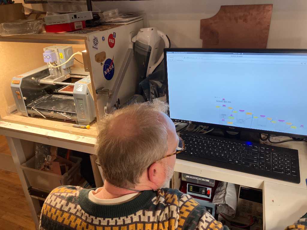
Roland Modela MDX20
Erwin gave us a workshop how to work on the Roland Modela PCB that is available at WAAG.
Machining PCBs is done out of FR1 or FR2 base material that has a copper plane on it.
FR4 vs FR1. No FR4 is used due to glassfiber dust particle health hazard
It is vital that the workbed is fully perpendicular to the drill bit. Also the PCB base material should be completely flat on top of the sacrificial layer which should be perfectly flat on the workbed.
We’re going to use 0.4mm tapered bits (it’s actually 0.25mm but because it’s tapered you’ll end up with 0.4mm) and V-bits (which is 0.1mm).
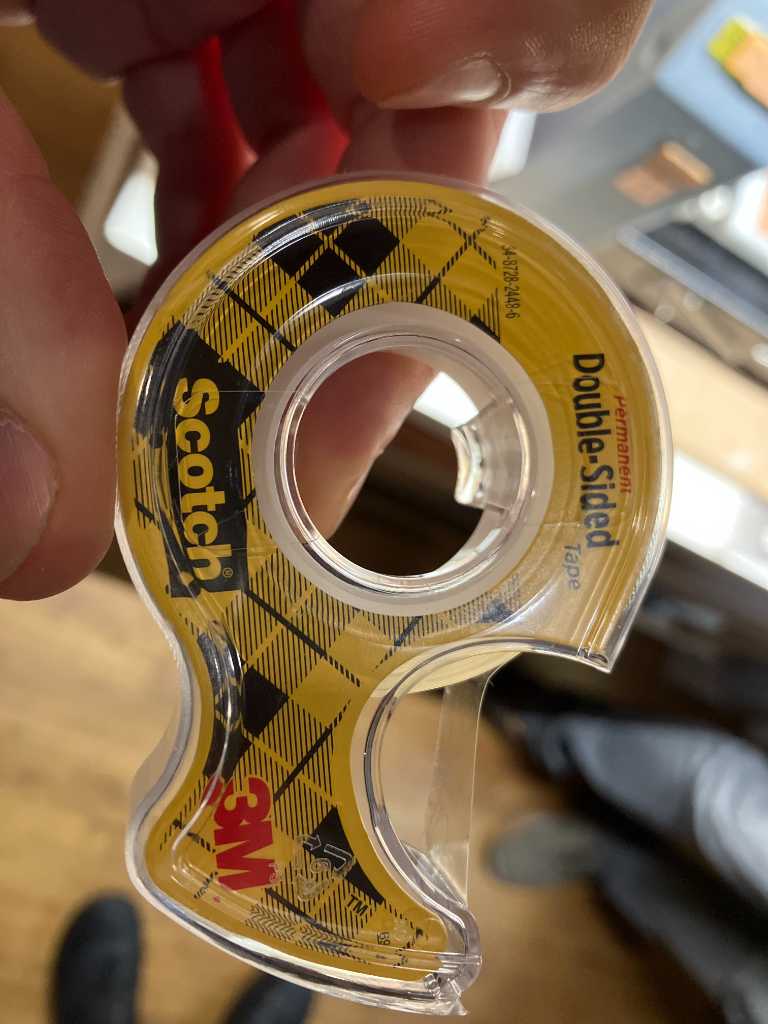
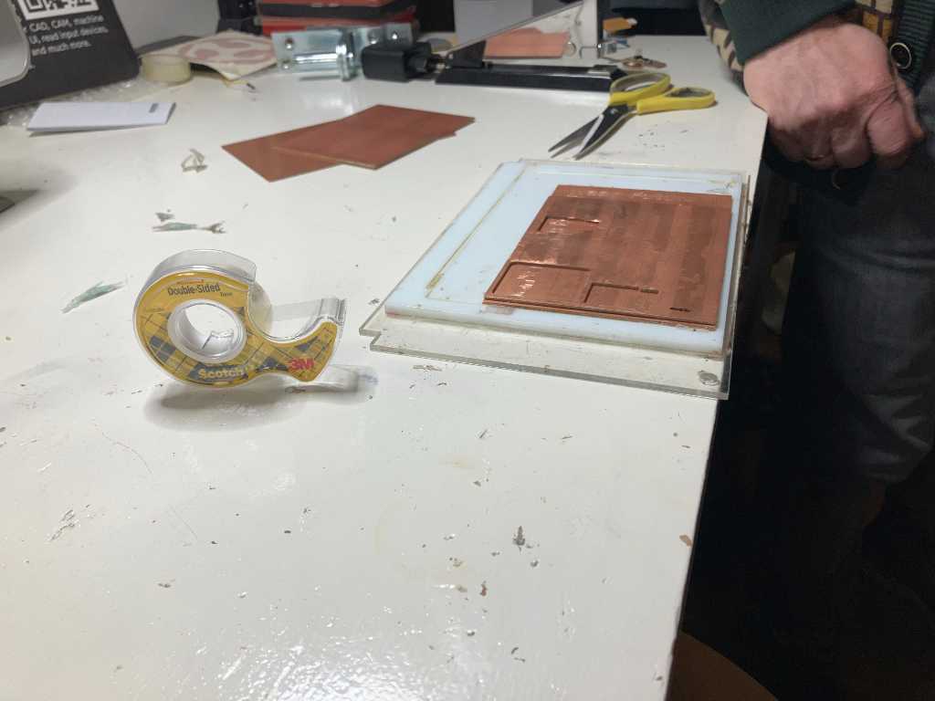
To get the PCB base material flat onto the machine, we’re going to use 3M double sided tape. No overlays obviously.
Hand soldering requires more clearance. Best is to use a clearance of about 1mm (4 traces of 0.4mm with 0.5 overlap) around pads. This is because we can’t apply solder mask.
We’re going to use mods to drive the Modela. Mods has default settings for the mill bits that we’re going to use. The design is in PNG format. Mods will convert this into milling paths.
This is the Modela:
waag modela documentation here
The white part is flattened by the models machine. So exactly perpendicular.
Waag uses an FR1-plate as sacrificial layer.
Always first reset the machine by pressing up and down button simultaneously. When the LED stops blinking reset is done. If something goes wrong and you have to cancel, you should also cancel in mods (by unplugging usb).
Press view mode to switch between setup mode and operation mode. In operation mode the board will go to the back. This is easy to reach for the spindle. But more dangerous because the machine will accept commands and might start operating.
Trying to remove a pcb is a hard job because 3M tape is sticky ;-)
More tape to take off. And to re-apply.
The full stack: baseplate, perfectly flat and perpendicular milled workbed and sacraficial PCB:
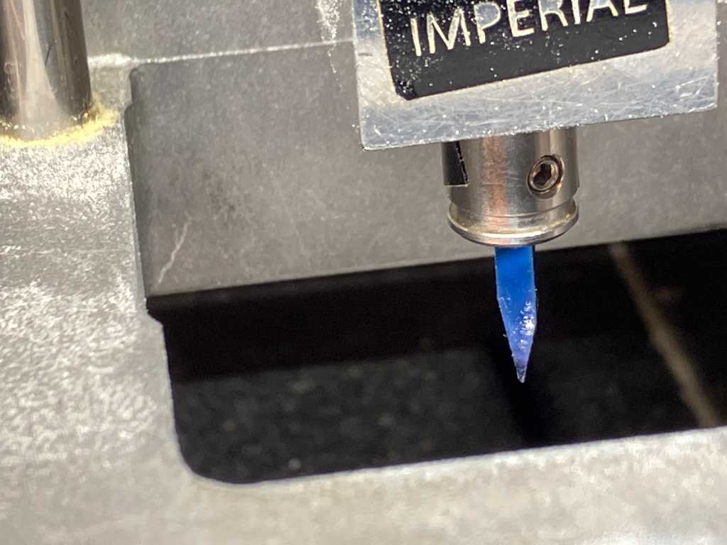
Unscrew the Allen bolt to release the bit from the collet. Currently there’s a v-bit in here.
When inserting a bit, put is high into the collet but not all the way. We’re going to use the zeroing procedure to get the correct length.
Overview of bits:
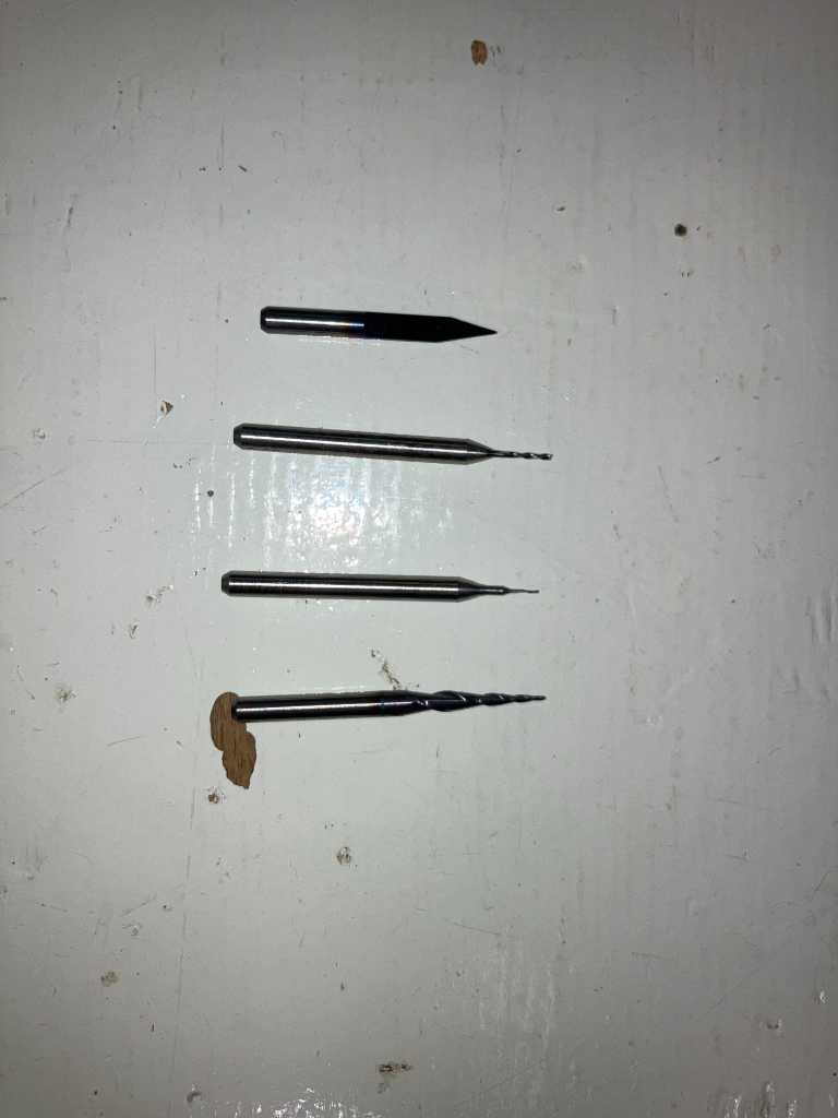
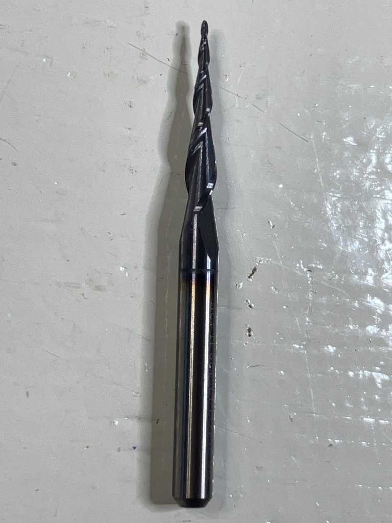
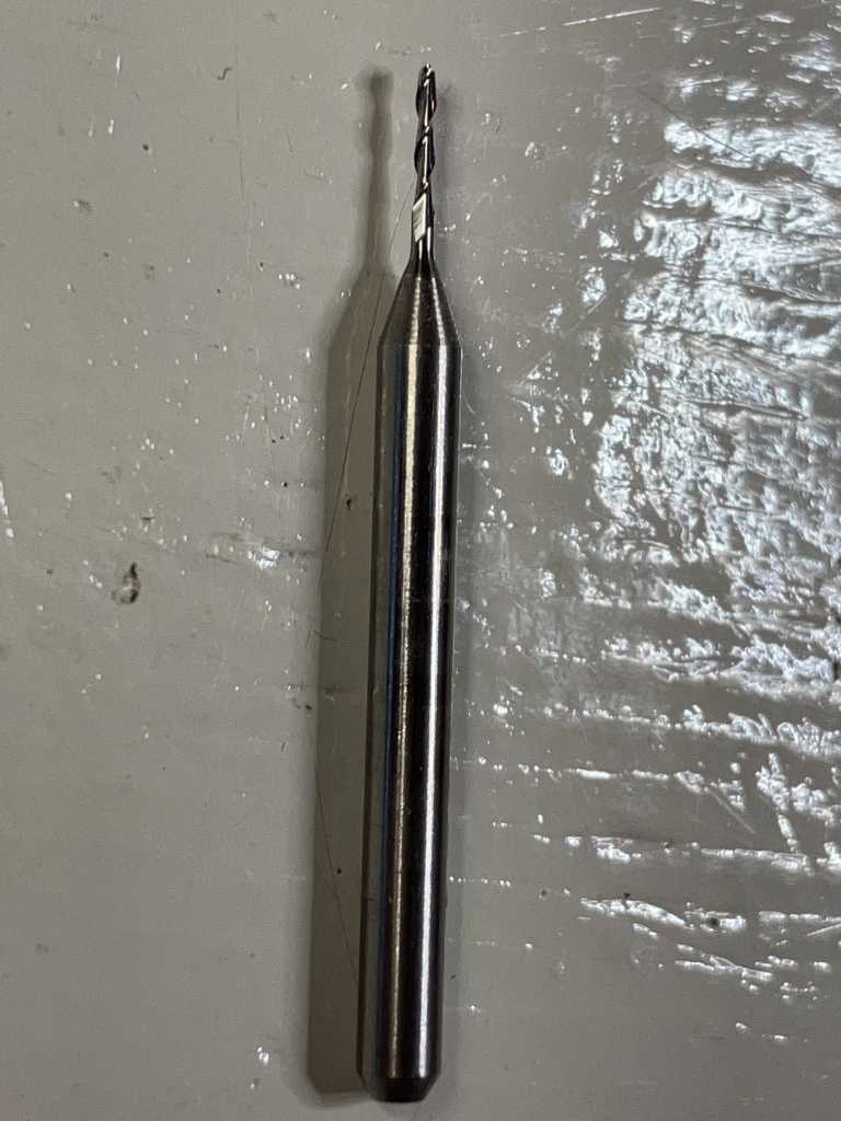
0.1mm V-bit with 30 degree angle, 0.8mm end mill, 0.4mm end mill, 0.25mm tapered bit (ball nose, 15 degree angle)
The end mills have 2 flutes.
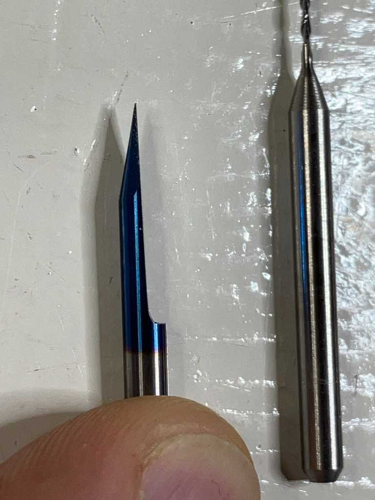
The tapered bit is a ball-nose. The nice thing about this is that it doesn’t produce burrs. tapered bit is stronger than an end mill. A V-bit produces more burrs.
Erwin working on Mods:
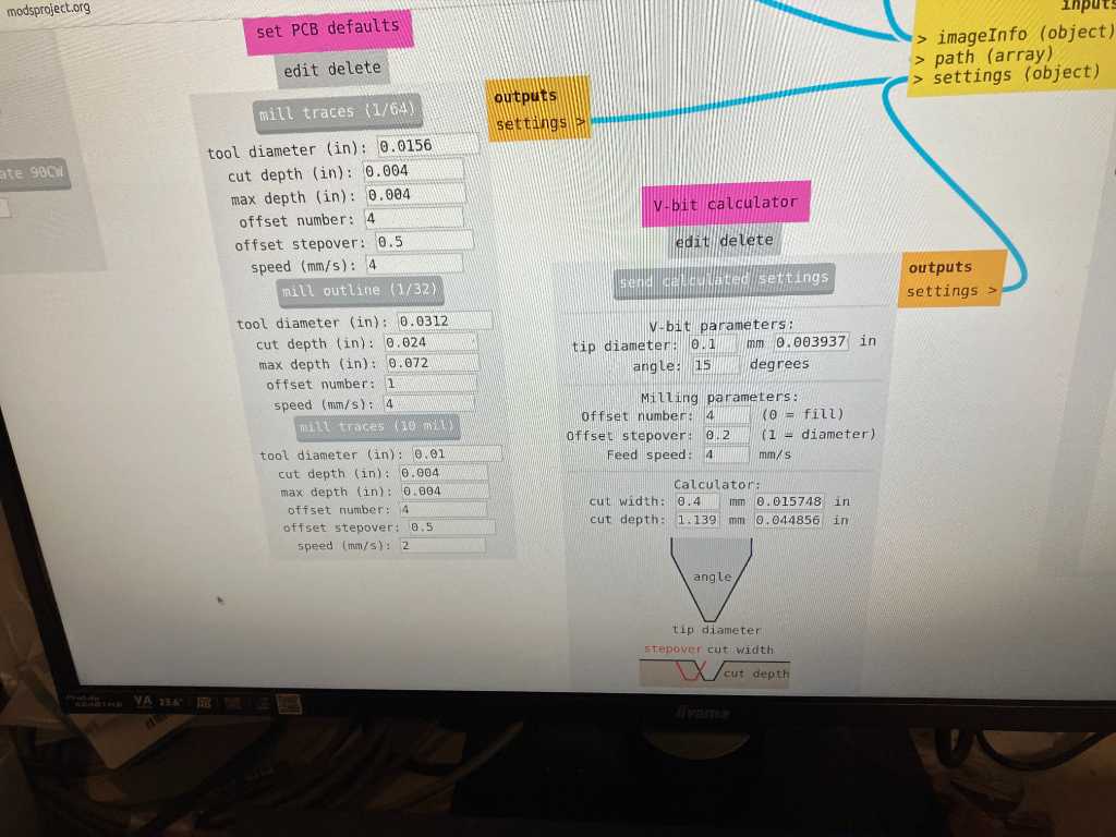
Default settings for different bits are in the mods program.
For tapered bit use the V-bit calculator block with these settings:
- tip diameter 0.25
- Angle 15 degree
- Offset number 4
- Offset step over 0.5
- Feed speed 4 mm/s
- Cut width 0.4 mm
- Cut depth 1.139mm <- wrong! Should be 0.254mm <- turns out to be too deep as well.
Next click “send calculated settings”. It’s send the correct values to the mill calculator.
Connect to the machine using the web serial block.
Use the Roland MDX block to move the head of the machine on X and Y direction (after connecting of course) by changing the X-origin and Y-origin. Record the X and Y coordinates because these will be your origin points!
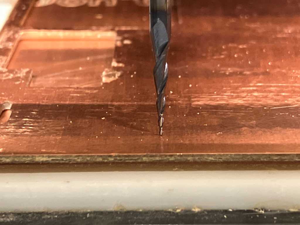
Next is the Z-leveling. Move the milling bit above the copper. Lower the head of the modela using the down button on the machine. Don’t use the software for this. Lowering it on the machine will immediately set this position as it’s zero position.
Next hold the bit and open the collet. Let the tool slightly touch the copper and fasten the collet again.
The zero is always bottom-left!
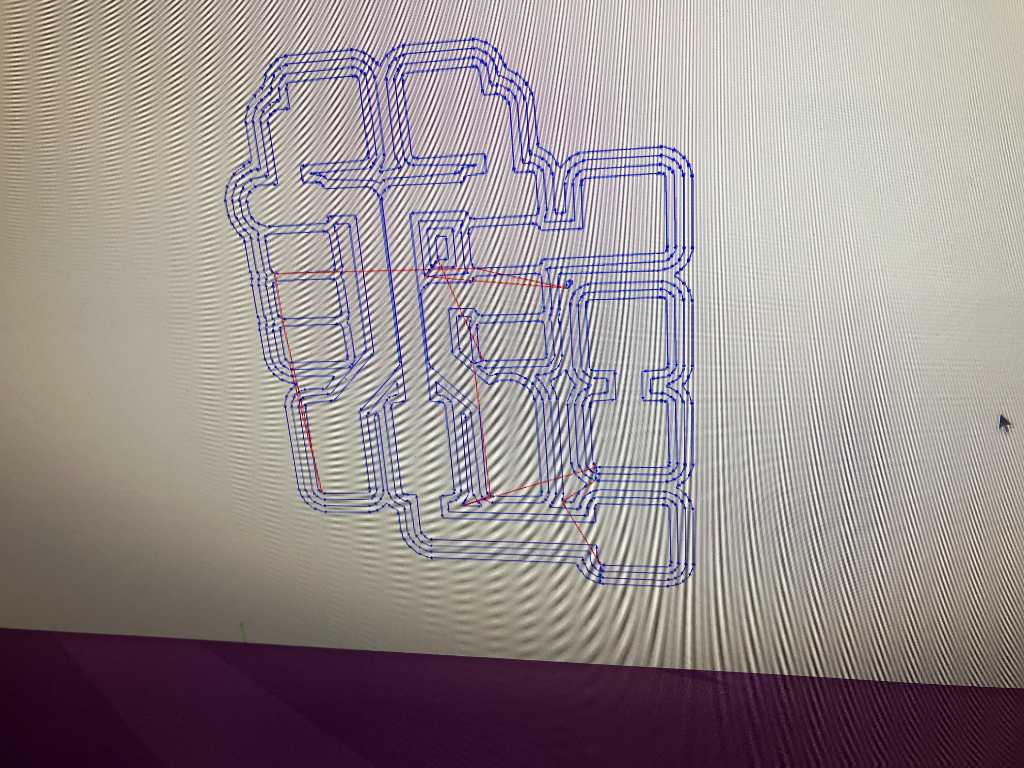
Time to load the file. PNG files with 1000 dpi will be perfect to use. Use the Read PNG block for this.
2 files are required as minimum: one is the traces and pads, the other is the cutting outline. All parts in white will stay. Not all black will be milled away because that will be to costly. It’s just outline the white parts.
Press the recalculate button on the “mill raster” block.
This image will pop-up showing the milling paths:
Finally go to the webserial block and press send file. The machine will start immediately. Use the View button as the pause button if needed.
When done use the vacuum cleaner to clean the board.
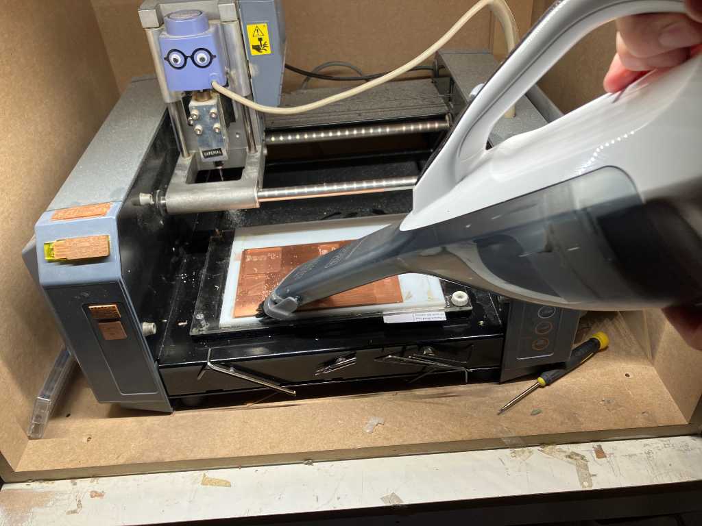
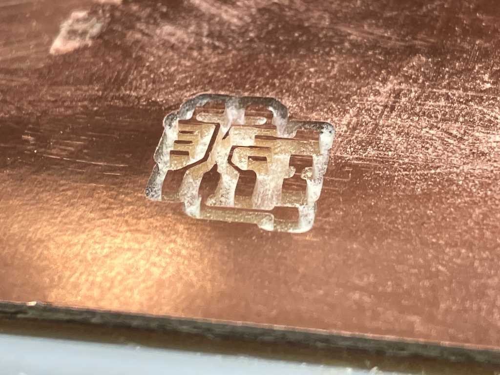
The result: the cuts are way too deep. #fail Somewhere down the line we made a mistake. We found out that we didn’t change the cutting depth. We use the v-bit block for a tapered bit. The default cutting depth is fine for a v-bit but much too deep for a tapered bit.
Next attempt is better in terms of depth but lots of burrs and a lost trace in the middle! #fail this most probably means it’s still cutting too deep.
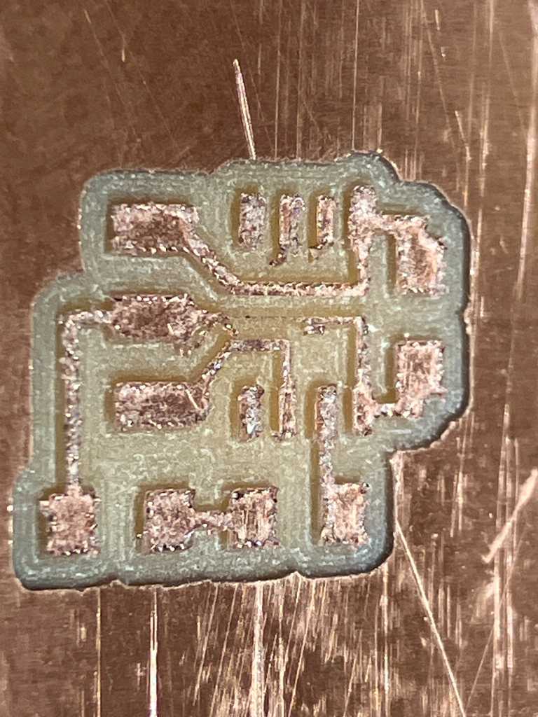
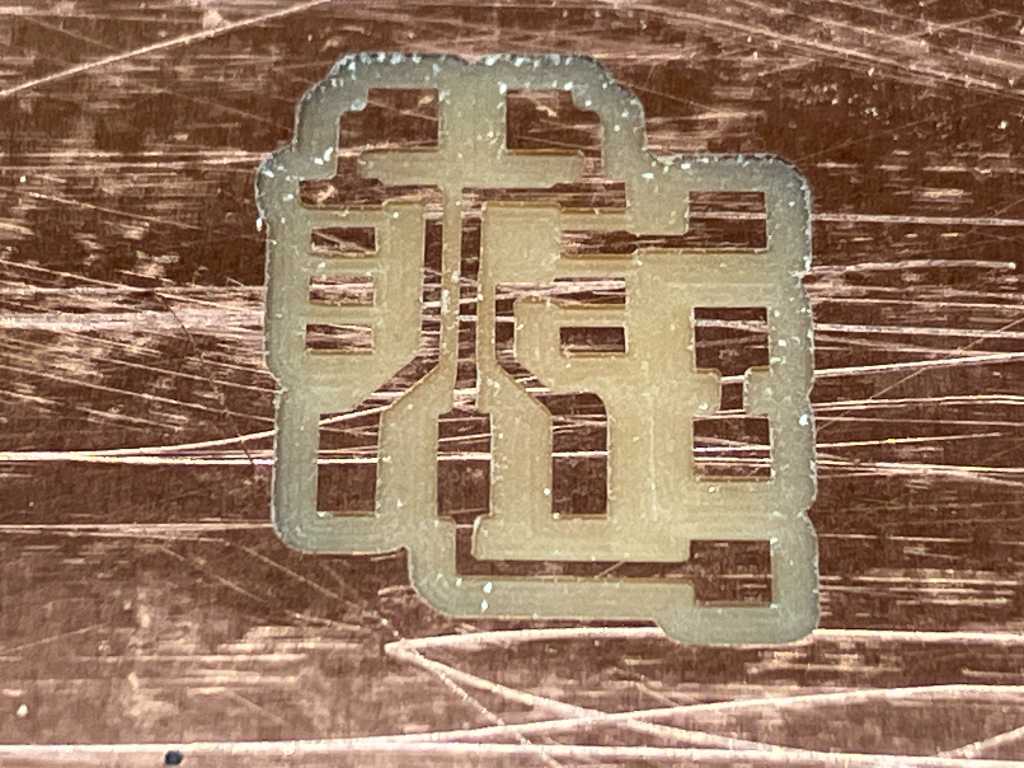
Let’s try an end-mill. Settings:
- 1/64 default
- Tool diameter 0.4mm
- Cut depth 0.003 inch
- Max cut depth 0.003 inch
- Speed 4 mm/s
- offset number 4 traces
- Offset step over 0.5
Max cut depth is the total depth it is going to mill. The cut depth is the depth of 1 pass. The amount of passes is max cut depth divided over cut depth.
Nice!
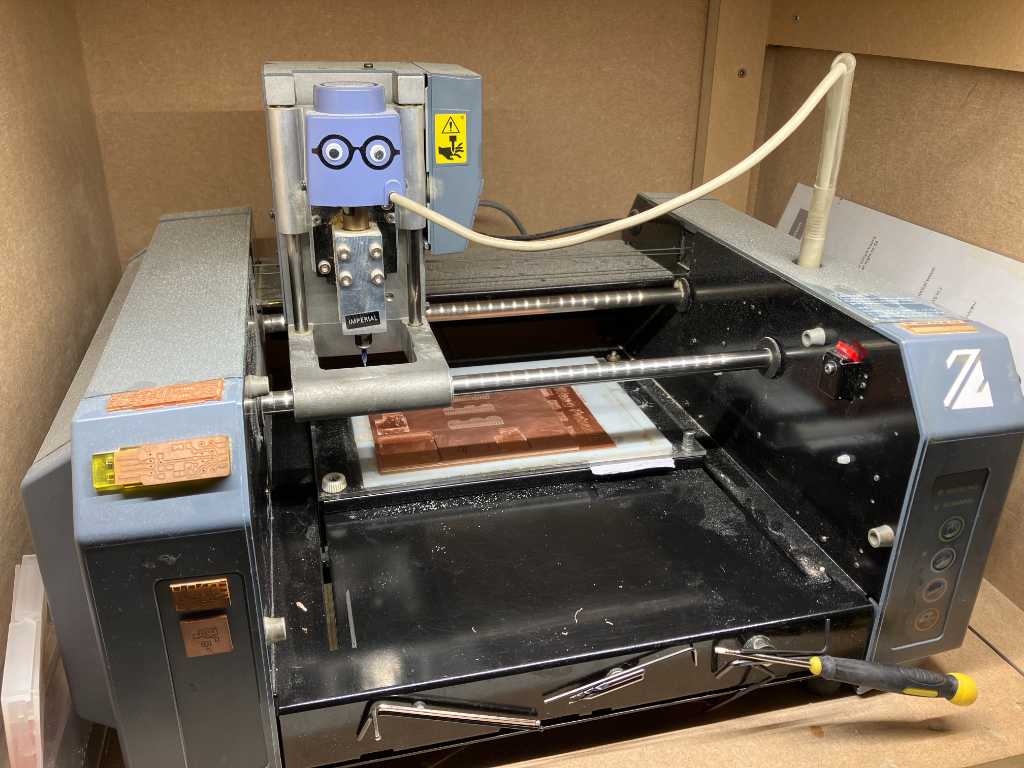
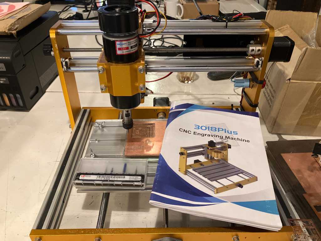
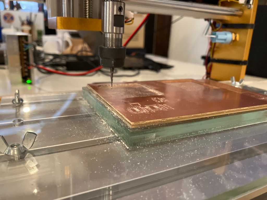
Lunyee 3018
Henk gave us a workshop how to work on the Lunyee 3018 that is available at WAAG.
This machine uses GCode as well. Difference is that for the Modela, the GCode is sent to the machine directly. With the 3018 you have to use a different program to actually load the GCode into the machine.
Use the Mods program G-Code -> Mill 2D PCB. It looks similar to the Modela program.
We’re going to use the tapered bit. So setting this into the V-bit block:
- tip diameter 0.25mm
- angle 15 degrees
- offset number 4
- offset stepover 0.5
- feed speed 4 mm/s
- cut width 0.3048mm (set this and cut depth is calculated)/
- cut depth 0.125mm (or set this and cut width is calculated)
It makes more sense to keep cut width constant and have Mods calculate the cut depth.
This Mods program doesn’t have a machine block. As soon as you press the calculate button, a GCode file is generated and downloaded by the browser.
Next is to send it to the 3018. The program to do that is called UGS (Universal GCode sender).
The Windows download binary uses a bundles Java. That is a big no-go in our University due to licensing issues. There’s a Universal Download as well. You should install your own java runtime environment. I’ve talked to our IT department and as an alternative they suggest using [Eclipse Temurin OpenJDK](https://adoptium.net/temurin/releases/. As we dont have a 3018 in our fablab, I haven’t tried this. But I did want to document this link.
Uploading is done via usb cable connecting to your computer.
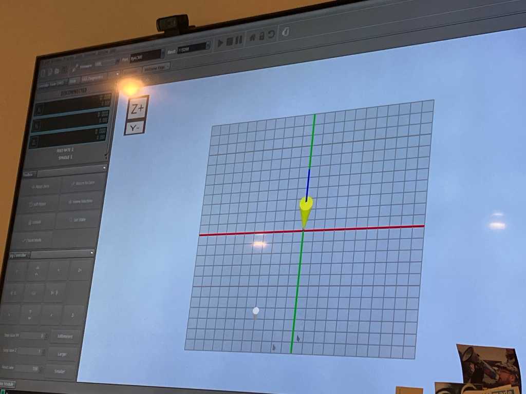
First connect the machine. In the jog controller section (bottom right) there are buttons to control the machine. Everything is in metric yeah!
Origin is bottom-left again. Set the machine to your intended origin and click the blue X and Y buttons on the top right.
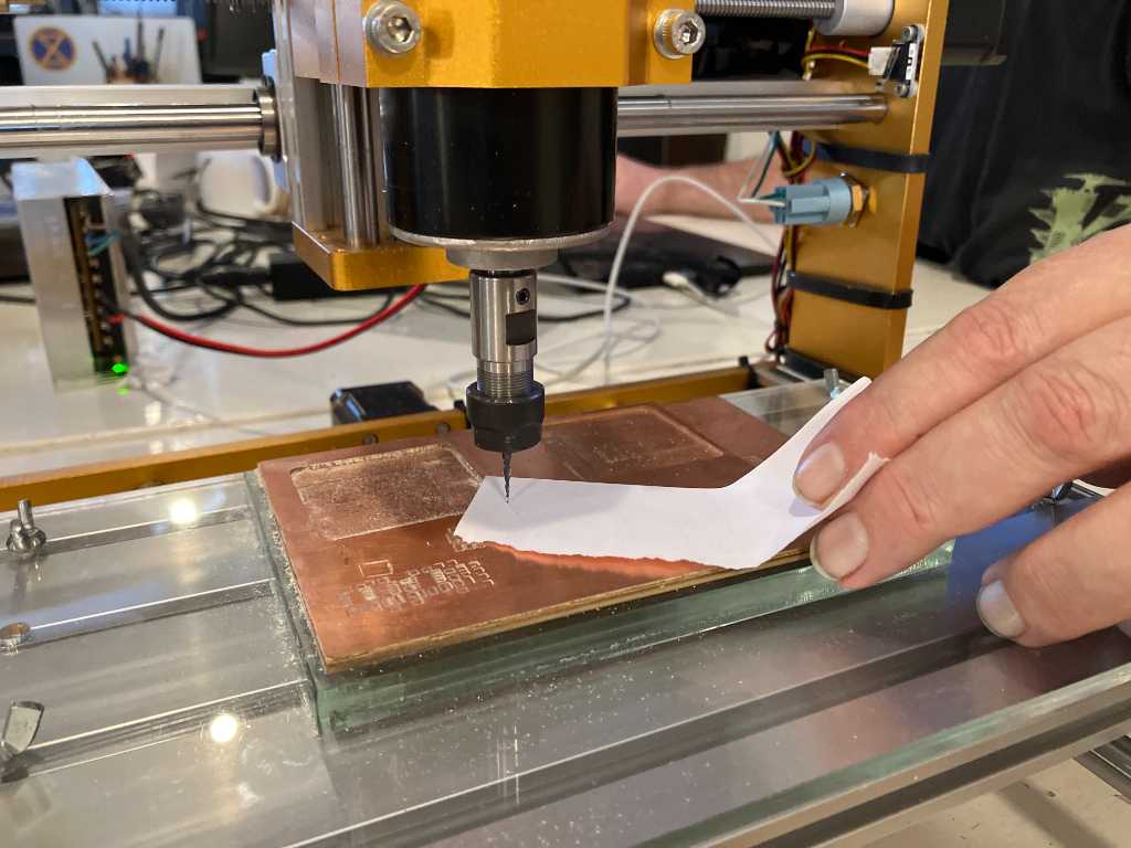
Next up is the Z-axis zeroing. The 3018 doesn’t have a set screw. You’ll have to use a fastening tool which is a bit rough. So we’re using a piece of paper to do the zeroing. Use a step size of 1mm and use the software to go done little by little. Last steps are done with step size 0.1mm until the paper is “stuck”. Then remove the paper and drop down another 0.1mm. Finally press the Z button in the software to set this as your zero point. Done!
Load the GCode that was generated by mods. And hit the play button.
The software has feedback. Blue lines are still to do, grey lines are already done.
Maybe a bit too deep but all traces are there. So pretty good.
Next is the outline. This is a different file to load. Same bit settings, but other settings:
- cut depth 0.23mm
- max depth 1.6mm (thickness of the PCB)
- offset number 1
- step over 1
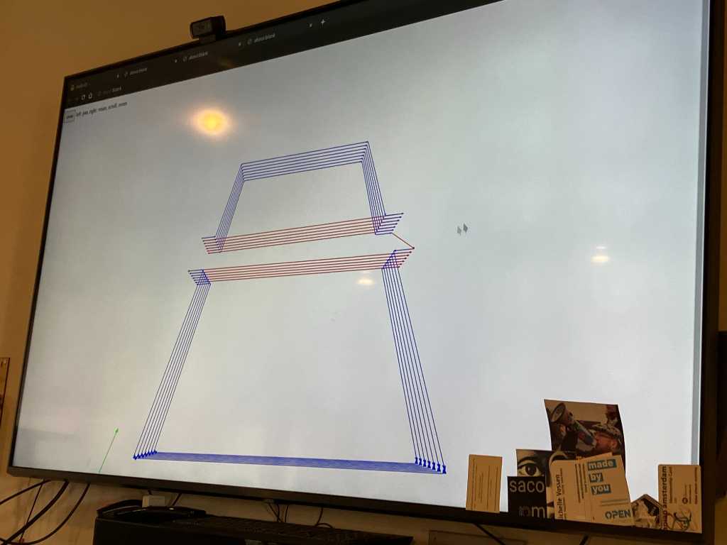
Tabs are not needed because the board is taped. But if you want tabs you can add them in Mods as well. This is how the GCode looks when tabs are enabled:
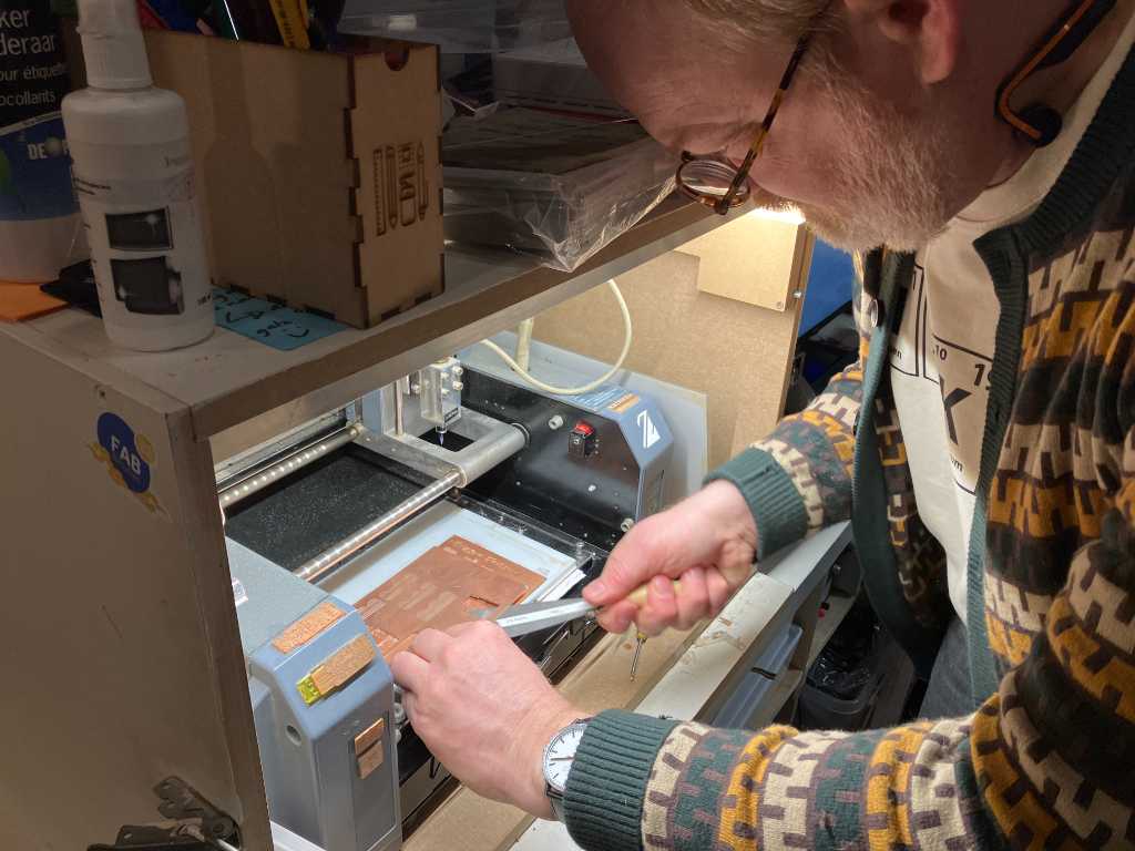
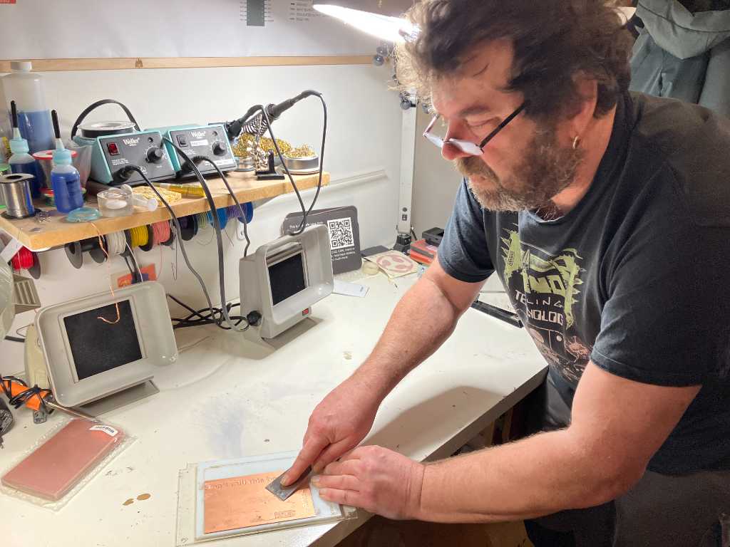
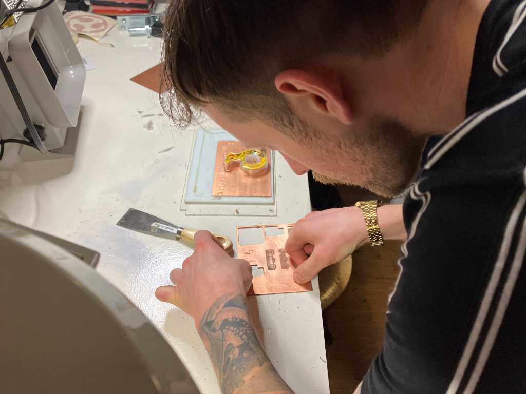
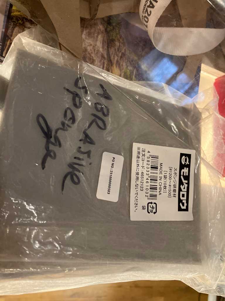
Use a wet sanding sponge to clean the PCB and deburr a bit.
The final piece:
Group assignment
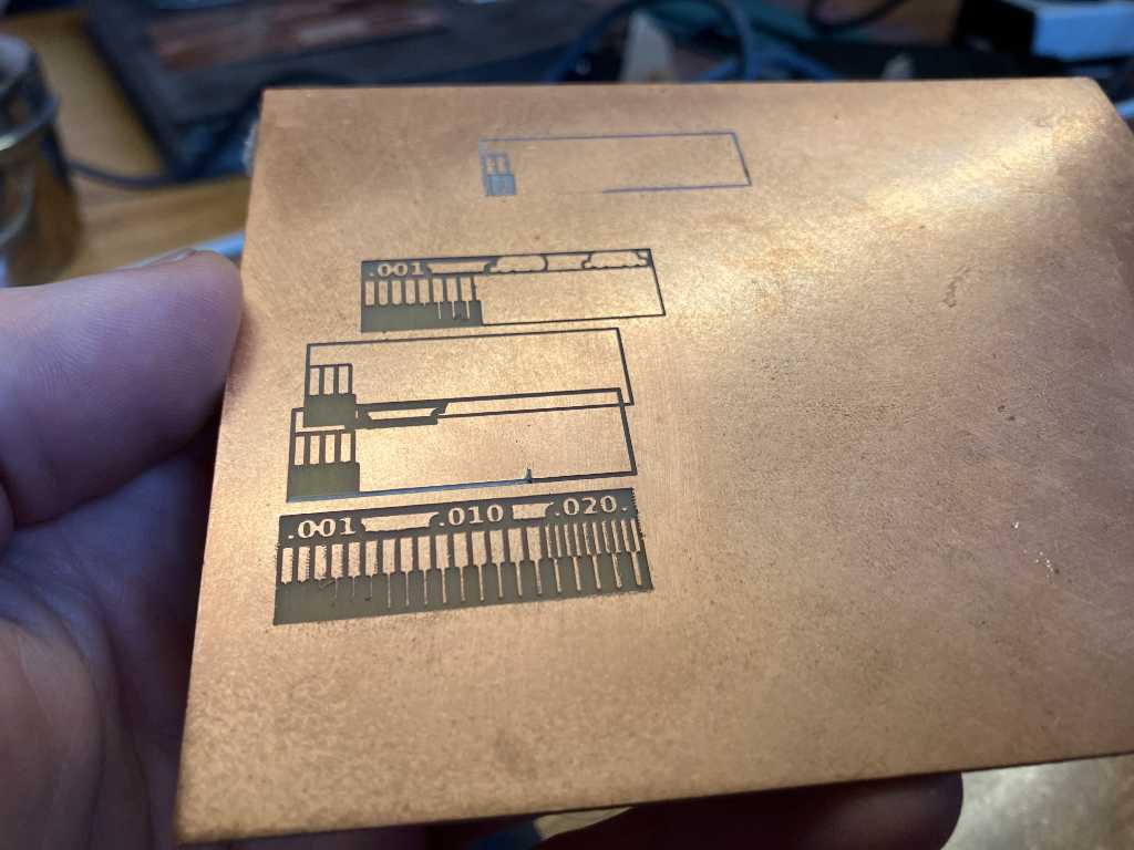
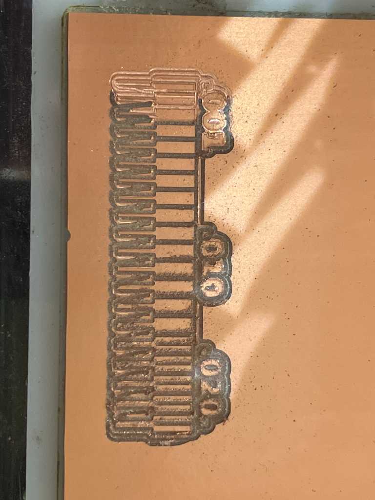
Together with Joe we’re going to try the traces test on both the Modela as well as on the 3018. Using all 3 bits (V-bit, Tapered, End mill). The file can be downloaded here.
Lunyee 3018
We started with the 3018. The documentation is done on Joe’s page.
End result:
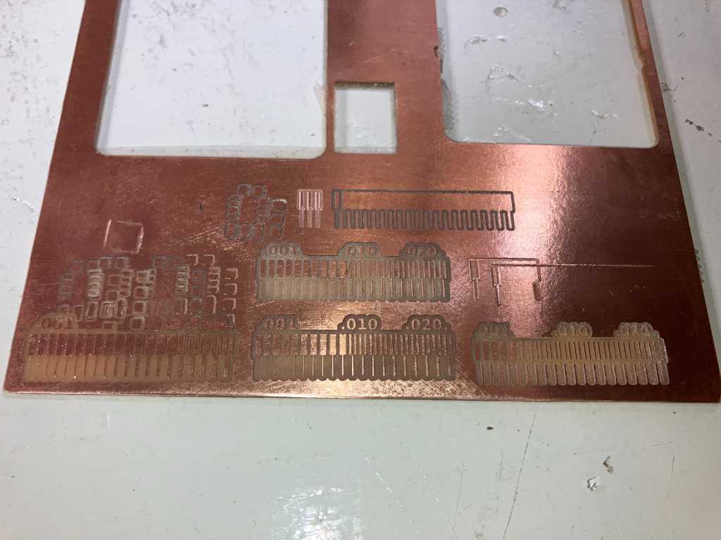
On the left: 0.4mm end mill
middle bottom: tapered bit
middle middle: tapered bit <- best one
others: #fail
And even the smallest trace made with the end mill is conductive!
Modela
Next we did the Modela. I’m documenting our groupwork here.
In Mods we have to select the proper USB port. It’s USB-Serial Controller D (ttyUSB0) (use Get Device in the WebSerial block).
Make sure the device is in view mode and add the PCB basematerial.
We start with the 0.4mm end mill.
Settings in Mods:
- tool diameter 0.4mm
- cut depth 0.003 inch
- max depth 0.003 inch
- offset number 4
- offset stepover 0.52
Click calculate and check the view. See if the milling traces look OK.
Next click the View button on the Modela to set it into operation mode. Otherwise it won’t move.
Next set the Origin by entering the X and Y values in the origin box and click “Move to origin”. We use:
- X 20mm
- Y 8mm
Next Use the down button to lower the Z. This will automatically set the Z zero position.
When almost touching the copper, loosen the collet bolt so the bit drops onto the copper. And tighten the bolt again. Things are setup now.
Press “send file” to start.
The result is not what we hoped for. We noticed that the bolts that tighten the sacrificial layer to the workbed came loose. Perhaps due to vibrations. We tightened them midway so that’s maybe why the left side is not good. But also we see some leftover that should have been milled away.
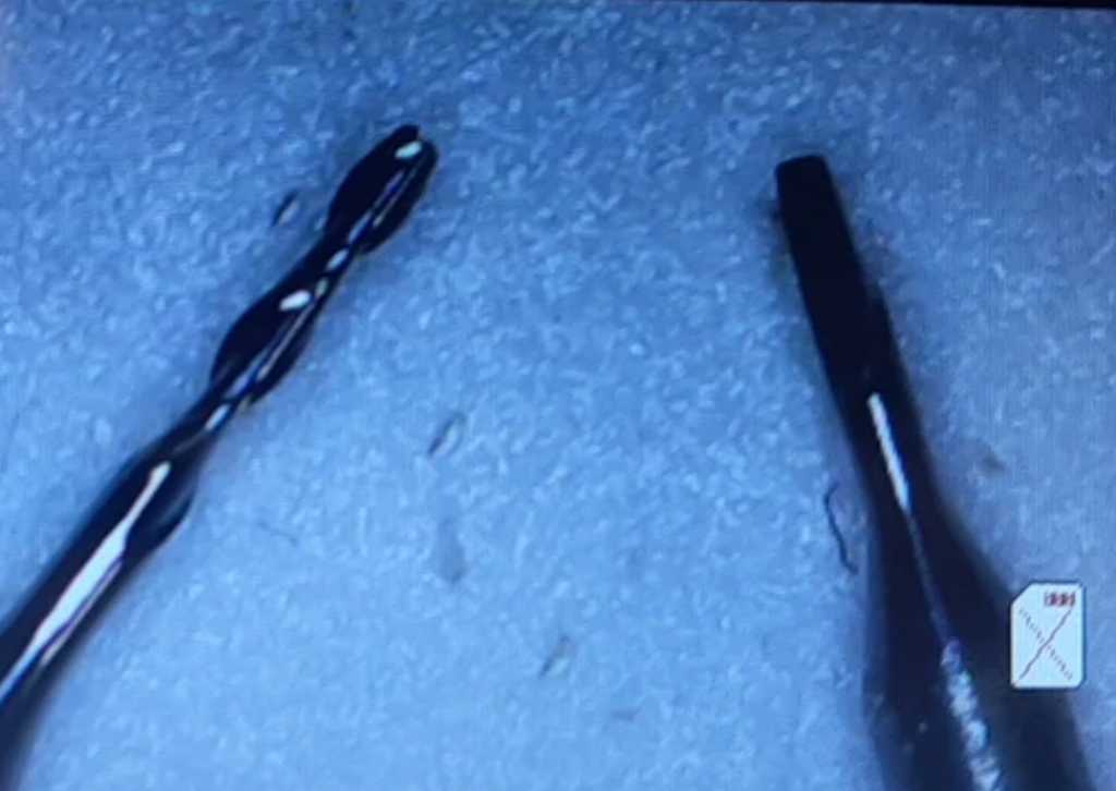
We had a final discussion with the 2 groups and compared results. The other group (Edwin and Vera) had the same result on the modela with the end mill. Or actually ours is worse :-( We believe the end mill is blunt. We didn’t have time go for another round with a sharp bit though. We also had comparable results on the 3018.
The next day, Henk, Vera and Joe found out using a microscope that both the end mill as well as the tapered mill were heavily damaged.
So to recap: It’s interesting to see how these 2 machines can mill PCBs. Although the Modela seems to be more solid, the 3018 result is very good. And the machine is much cheaper. Having a go at multiple bits was interesting too. So far I’ve only used end mills in our fablab. I will stick to it too because it gives the best results. And our machine picks up & zeros the tools itself. So no breaking here. Still, great to do this especially to learn more CNC type machines. This is something that I know too little of and is one of my fabacademy goals.
As discussed with Henk we’re not going to send a file to a PCB board house. As we’re going to do this in 2 weeks: PCB design week.
Individual assignment
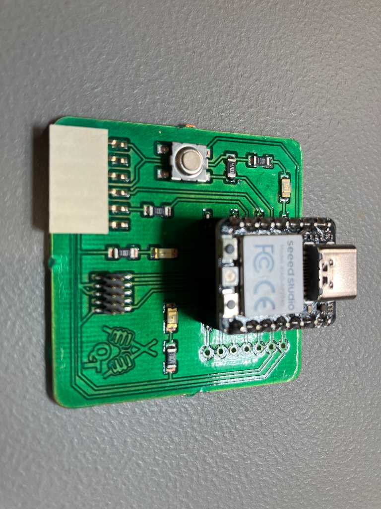
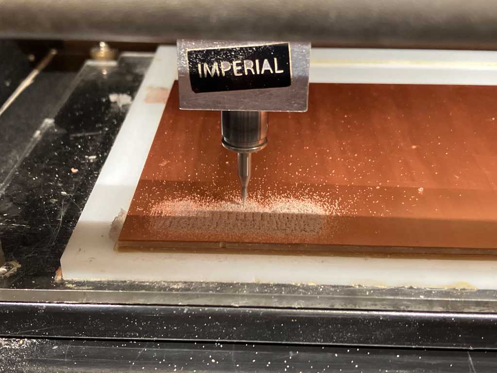
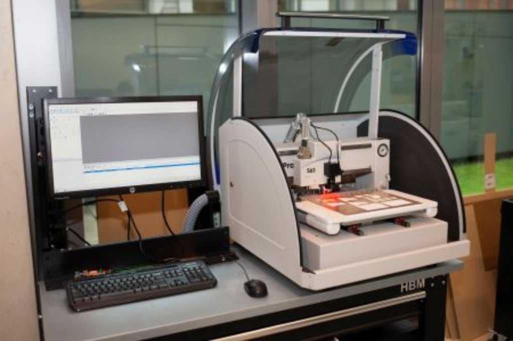
For my individual assignment I will be making the Quentorres programmer PCB using the LPKF S63 PCB-mill that we have in our Fablab. The LPKF as a dust extraction system with filters, so on this machine we are allowed to use FR4 copper clad.
The Quentorres is a microcontroller programmer that uses the xiao rp2040 from Seeed Studio as it’s brain. It can program AVR Series 1 and 2 and ARM microcontrollers.
There are 2 versions of the Quentorres. With V1 you solder the Xiao RP2040 directly onto the board. With V2 you use a socket to install the Xiao RP2040 onto the board.
LPKF CircuitPro software
The LPKF uses a software program called CircuitPro PM 2.5 to operate the machine (CAM). To be able to import the design into CircuitPro, I need to get them into Gerber format. Gerber version 2 (GerberX2) is preferred as everything is in Gerber (including drill files) and all layers (including layer arrangement) is clearly defined. With GerberX1, you’d also need an Excellon Drill file (NC Drill file). The excellon file has as main disadvantage that the Zeros format and drill units is not part of the file itself. So depending on who exported it using what settings, you’ll end up with something that might not fit.
The GerberV1 is available for download at the Quentorres gitlab repo.
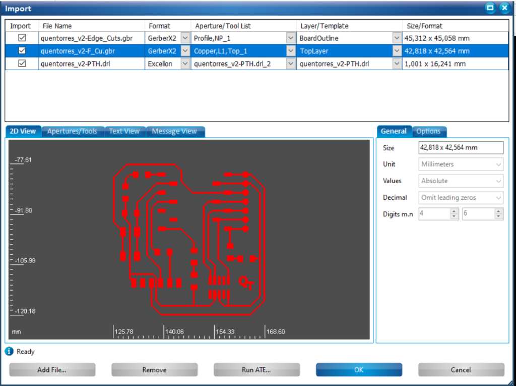
CircuitPro makes it really easy to import files. On the left the import window, on the right the result
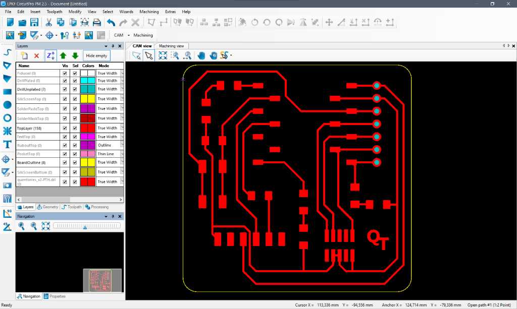
After creating the routing and drilling toolpaths. This can be send to the USB connected LPKF S63 immediately
So this was no fun at all, right? I’ve never used Kicad, so let’s find out how I can change the file a bit (custom logo?) and export myself in GerberX2!
opening QuentorresV2 in kicad v7.0
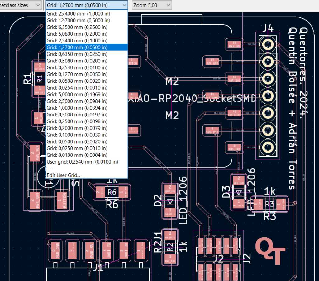
When opening the PCB design in the PCB editor I noticed that the design was not on the grid. This is always a difficult part: which grid to choose? I much dislike the imperial system. The world would be better of if we’d decide to use one unified well-defined system of measurement. Oh wait, we did in 1960:

source wikipedia
Anyway, lot’s of chips are still using imperial measurements, so it is advisable to use that as a grid. Unfortunately I noticed that none of the default grid values of kiCad would fit the Quentorres design. Not sure what they used as grid? This makes it harder to edit. As things will not snap to grid anymore.
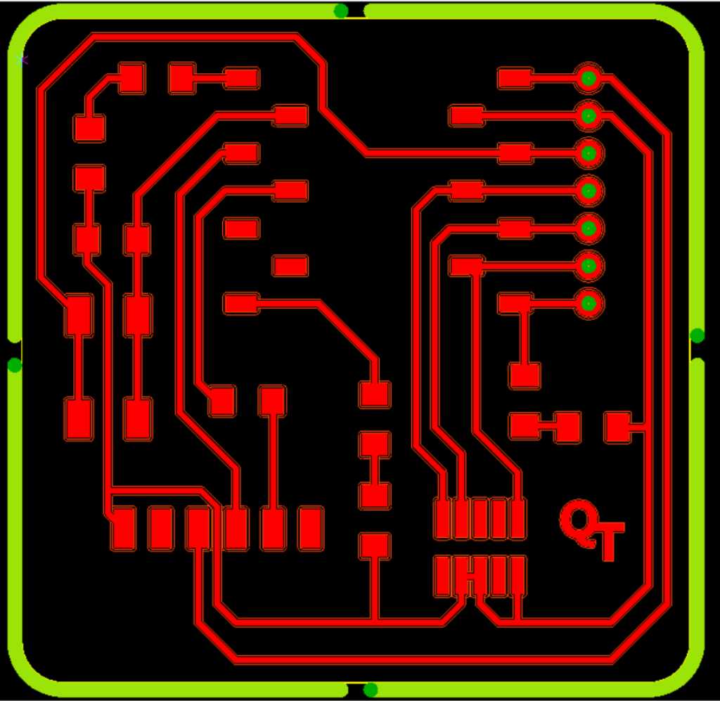
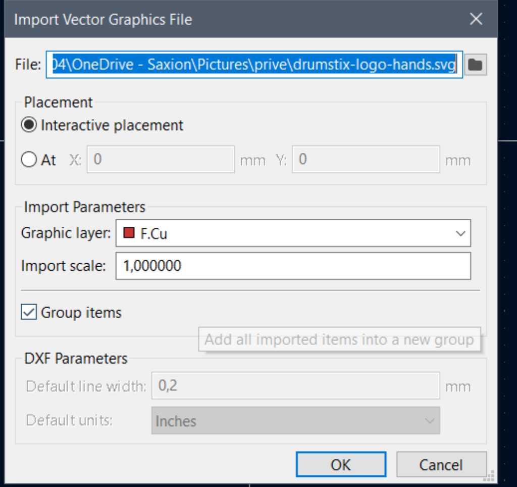
I edited the board layout a little bit to make space for my logo. I have my logo in svg file format, so need a way to get it onto the PCB. To do this I made a footprint using the kicad footprint editor. First I created a new empty footprint. Next I imported the svg using File - Import - Graphics. Make sure to select F.CU as graphic layer so the graphic is going to be made into the copper layer.
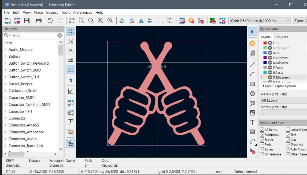
I had about 9x9mm space. So I made sure to use the import scale so the resulting size was about 9x9mm.
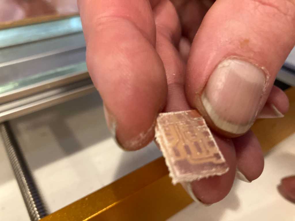
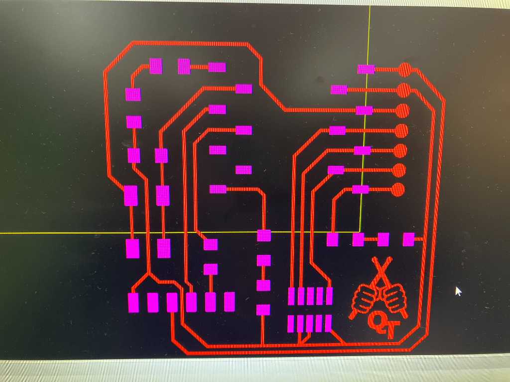
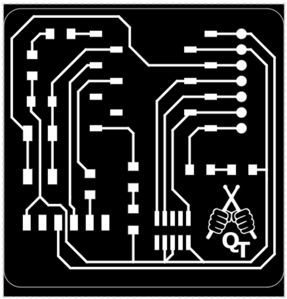
The resulting PCB:
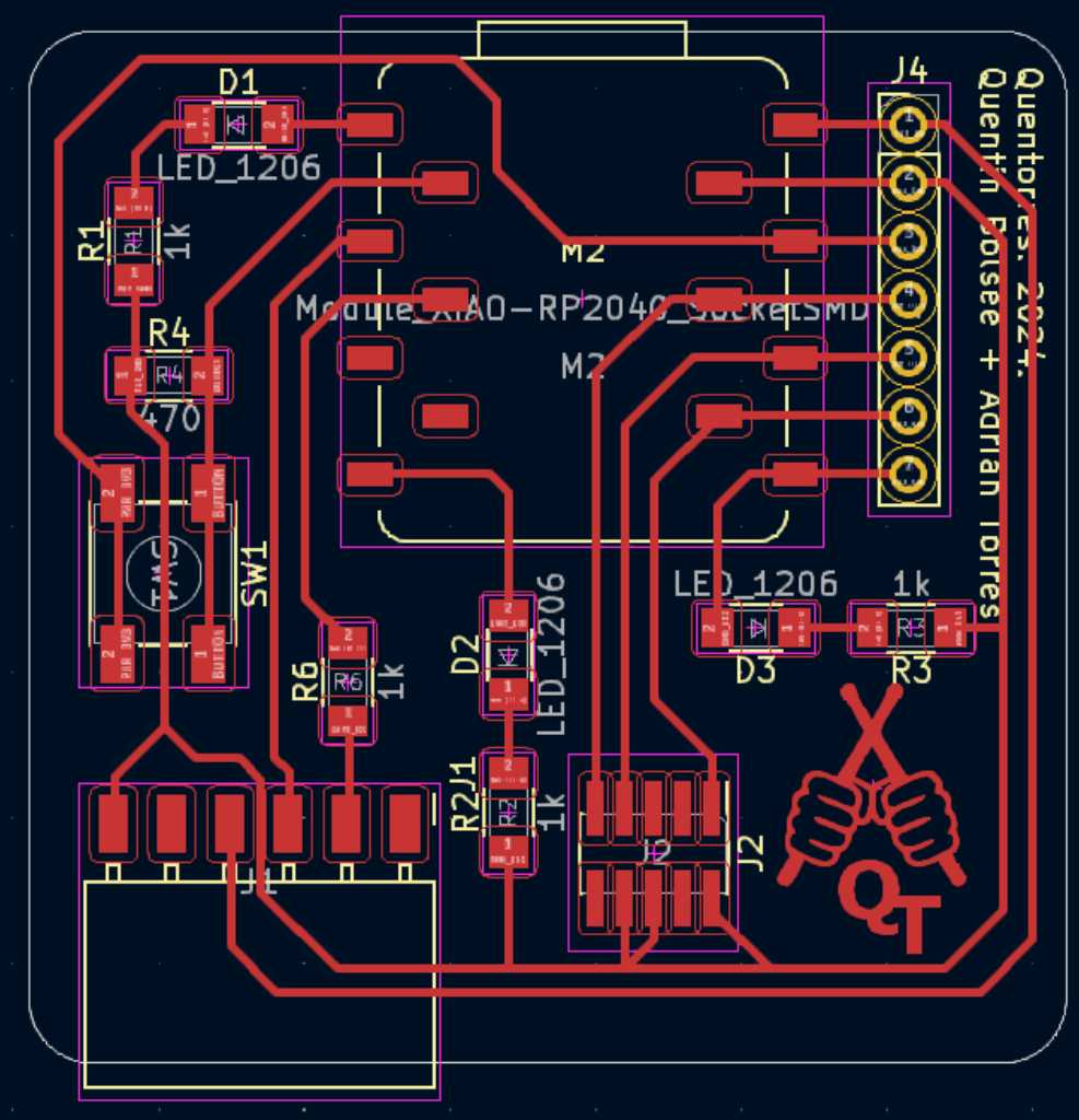
Next is to export this design as gerberX2. I do this using File - Fabrication Outputs - Gerbers.
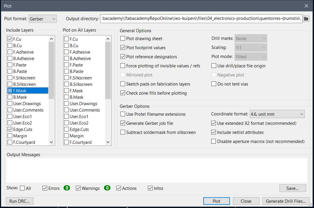
I’ve only selected layers F.Cu, F.Cuts. Next I click Run DRC. This is to check any design rule violations.
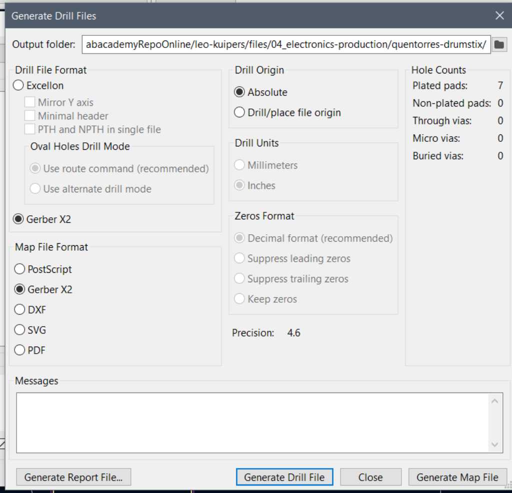
Before clicking plot, I first clicked Generate Drill Files. Here I selected Gerber X2 as output format. Yeah, everything is well defined now!
Next I imported the gerber files into circuitpro and here’s the result:
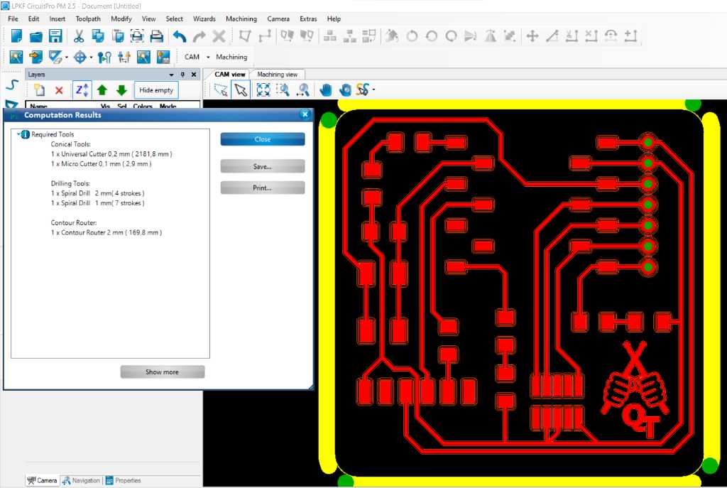
This means 2.2 meters of milling :-)
PCB Milling
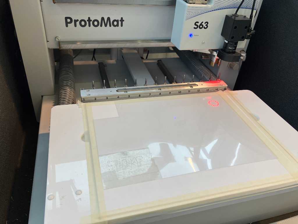
Getting our LPKF S63 is simply done by following the production wizard. It’ll explain to add the material to the machine, set position and start milling. The machine has an automatic tool change, so all production is easy.
LPKF S63 milling process, 48x speed
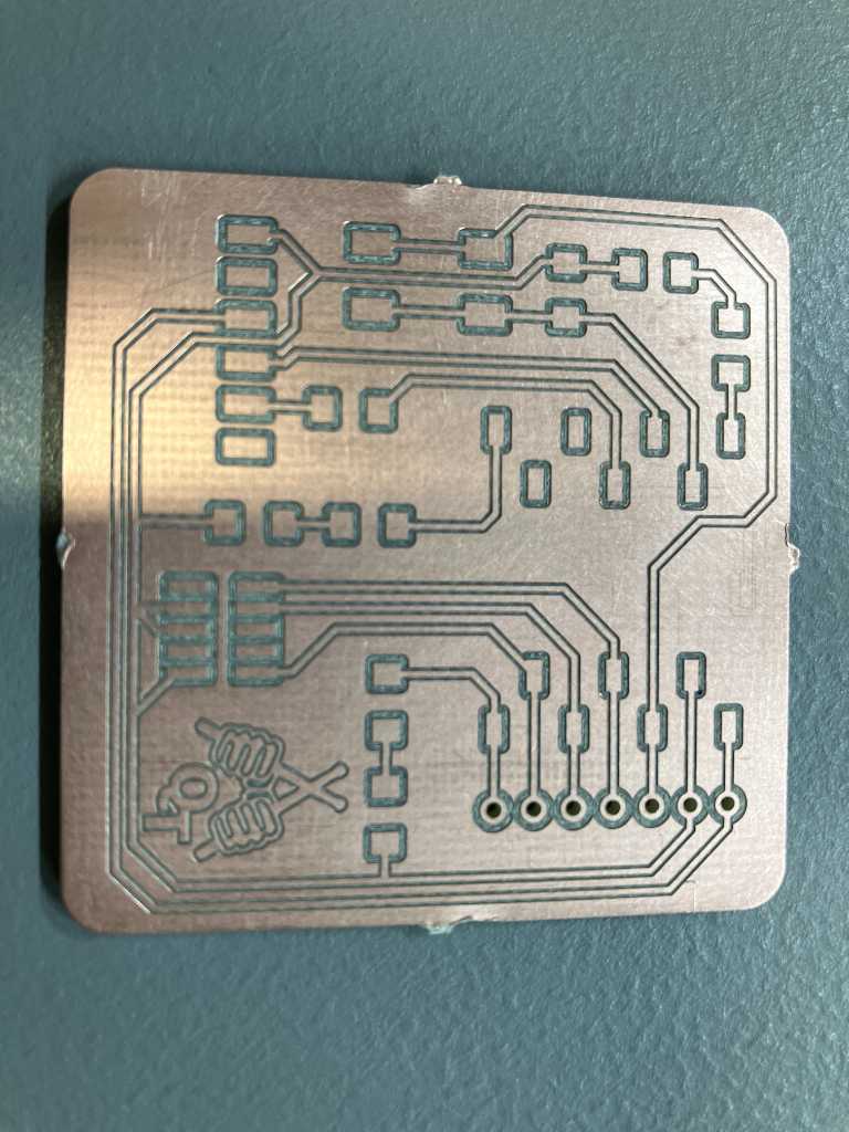
The end result:
Solder mask
Now I want to add a protective solder mask layer to prevent the PCB from corroding and to make soldering easier. Adding a solder mask is a bit of a chemical process:
- apply solder mask onto the PCB
- laminate
- cool the PCB
- Expose with UV
- Let it rest
- Etch using Sodium Carbonate
- Clean
- Final expose with UV
- Final harden in oven
Eventually I hope to cut the chemicals and use our laser cutter instead of etching. But the fiducial camera in our Epilog laser cutter somehow doesn’t properly calibrate (still work in progress) so I can’t do this now. I have to go chemical. Fortunately Sodium Carbonate is fairly safe to handle.
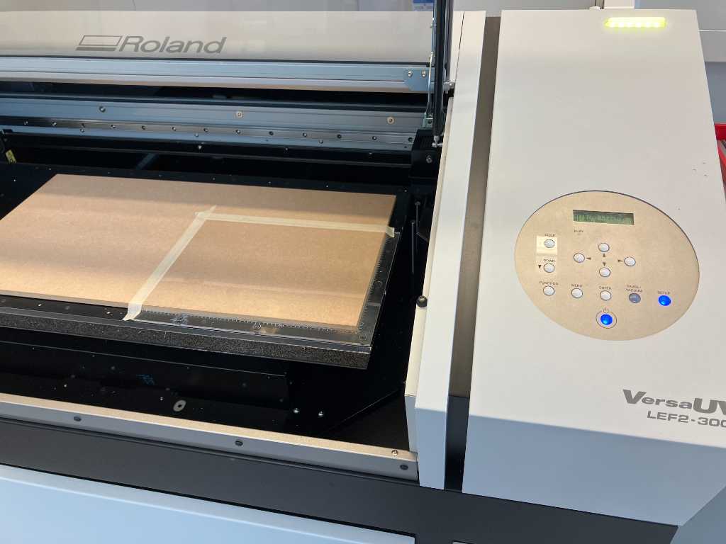
First I need to print the solder mask layer, because I’m going to need this in the UV expose step. I use our Roland VersaUV LEF2-300 UV printer for this, but it can be done on any laser printer too. I’m printing the solder mask layer in black, mirrored, on a transparent sheet.
Next I’m going to use Dynamask as solder mask.
I cut the green dynamask to size.
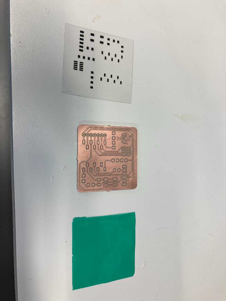
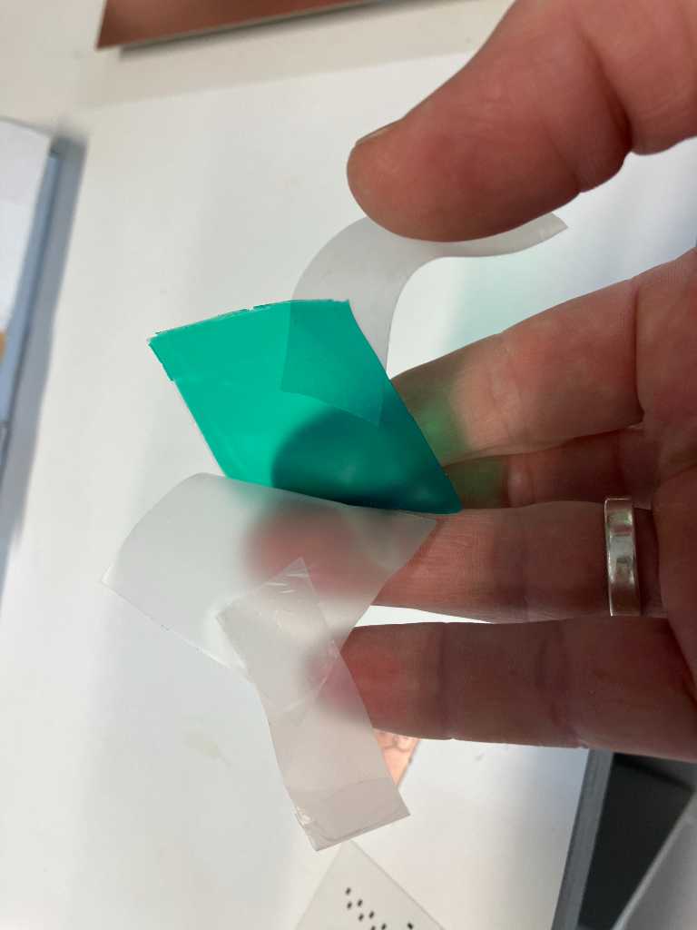
Next, I remove one side of the protective layers using a piece of tape. Dynamask has protective layers on both sides. In this stage you only want to remove one side.
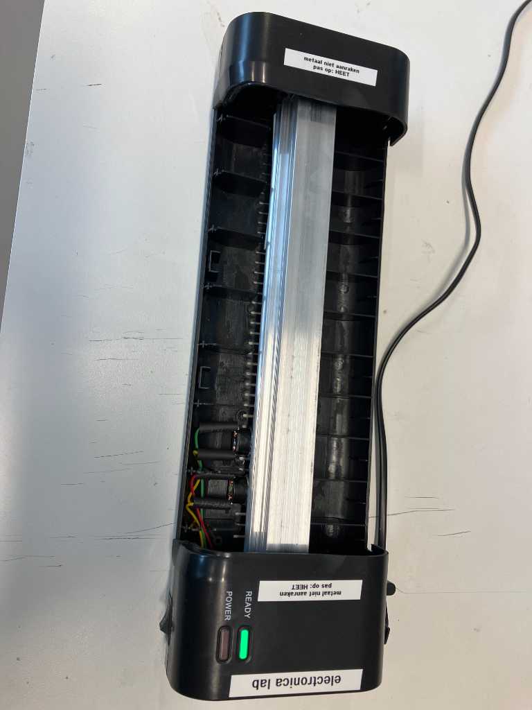
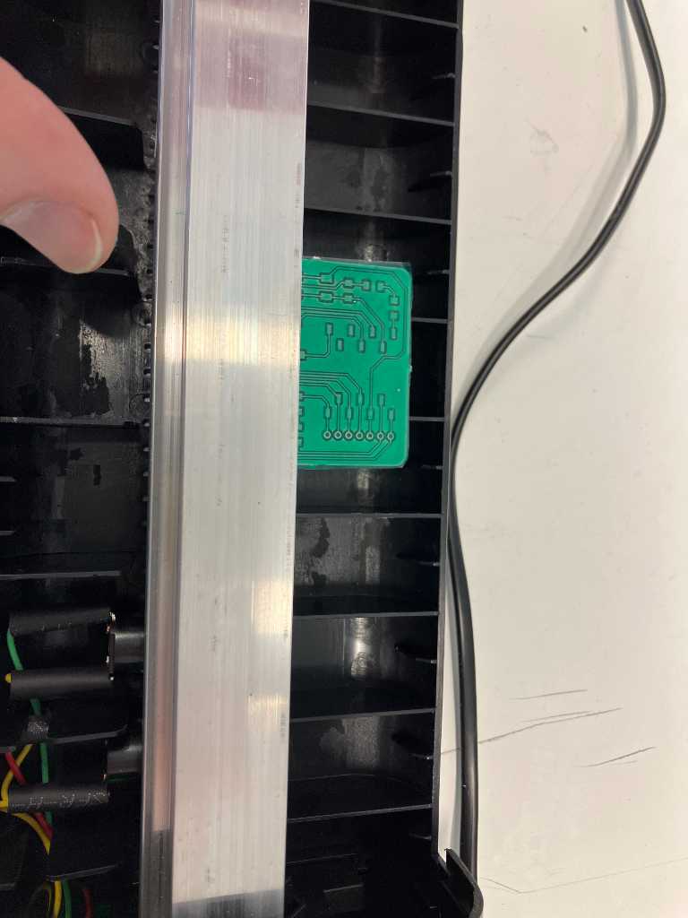
I’ve done this process before and so I’ve converted a cheap lamination machine so I can use it to apply the Dynamask.
Immediately after this, I cool the pcb using cold water and dry it.
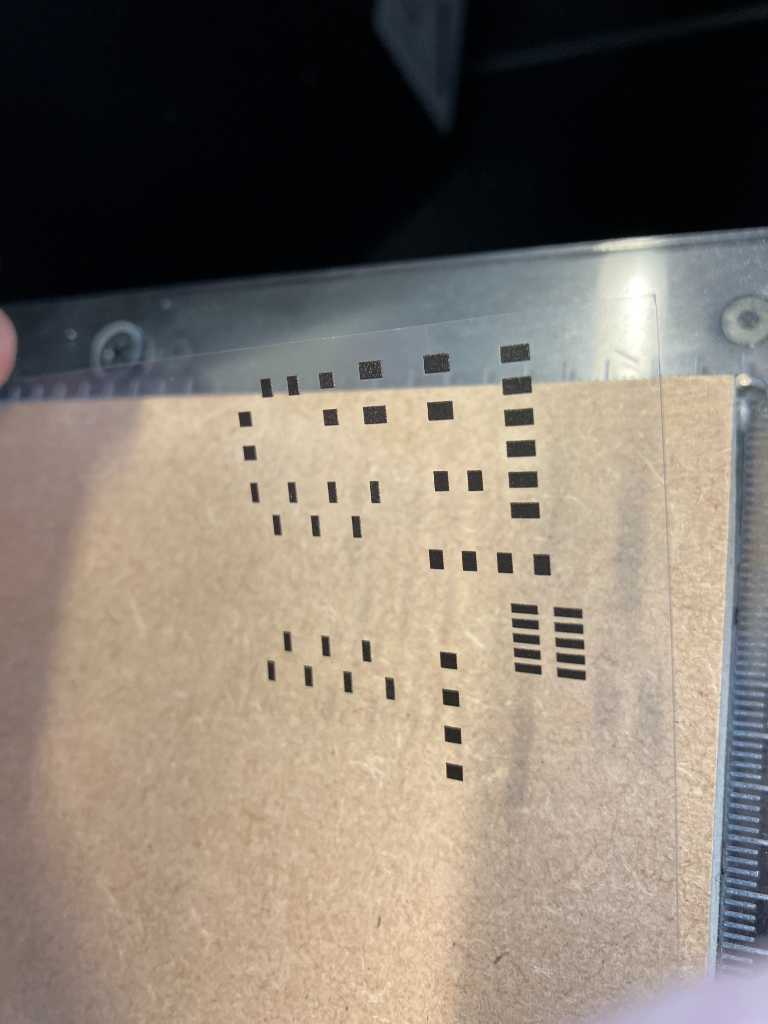
Next is the UV exposure phase for which I use the transparent sheet that I just printed.
I expose it 90 seconds in our 4x8W UV exposure box. And leave it to rest for 30 minutes.
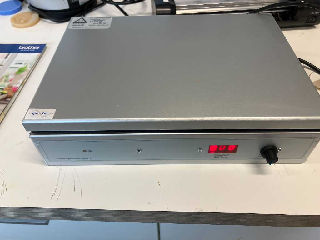
Gie-Tec UV-exposure box 1
Now I can prepare the Sodium Carbonate developer for the solder mask. I use 5mg of Sodium Carbonate and 500ml water. The developer should be around 45 degrees Celsius.
I take off the remaining Dynamask protective layer and develop the PCB with the dynamask, hoping that the solder pads will reveal.
Finally I do a final UV curing of 30 minutes and a final heat curing of 60 minutes at 150 degrees Celsius.
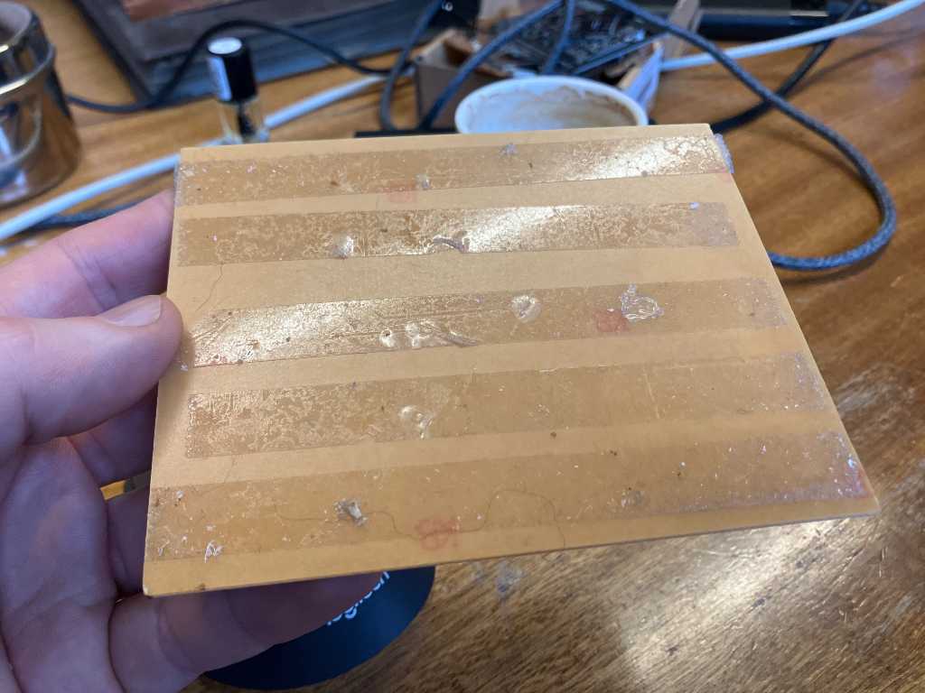
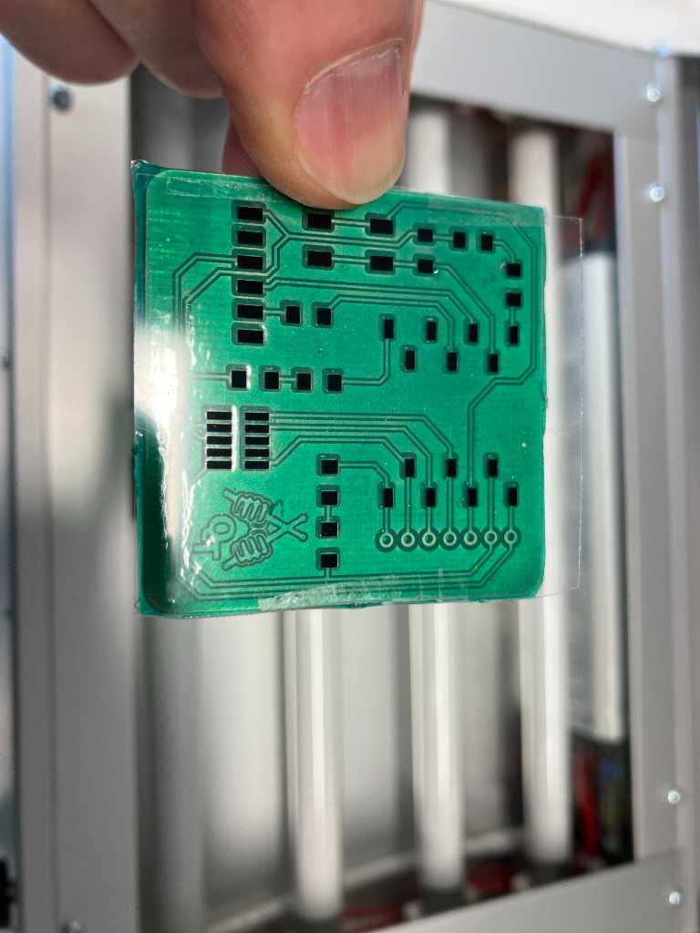
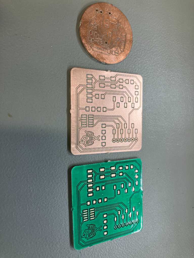
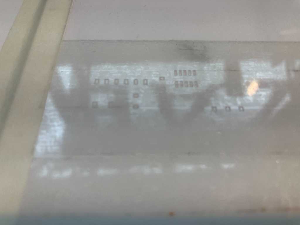
The end result: A PCB that I had lying around for quite some time with corrosion, a freshly milled PCB and the PCB with the solder mask.
Looking good but one #fail : the copper outlines of the through holes are covered with soldermask. Apparently my exposure sheet didn’t contain these pads… But this is not too hard to fix.
Solder paste stencil
So far I’ve never used a solder paste stencil. I just manually add some solder paste onto the pads. However the LPKF can mill a stencil, so let’s see if I can get that to work.
First I open Circuit Pro and use the template Stencil_size A4 for QR 266x380_Frame.cbf but I removed the frame perforation marks.
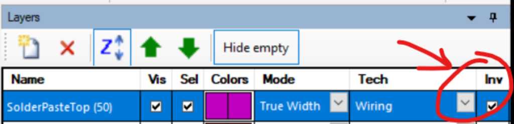
Next I import the solderpaste layer and make sure the inverse checkbox is checked. This will make sure that during toolpath generation, the inner path is generated instead of the outer.
No other actions are required, so let’s hit the production wizard button.
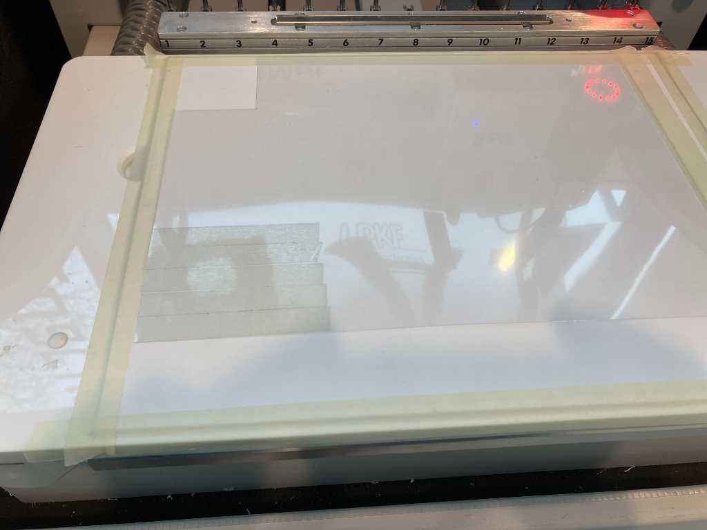
I don’t have a specific polyamide sheet in the Fablab, so I’m going to try to use the sheet that I used to print the UV exposure mask onto. It’s just a generally available transparent sheet with measured thickness of 0.2mm (200 micrometer). I think it will mill similar to a polyamide sheet so using those settings.
I’ve added it onto the workbed using doublesided tape:
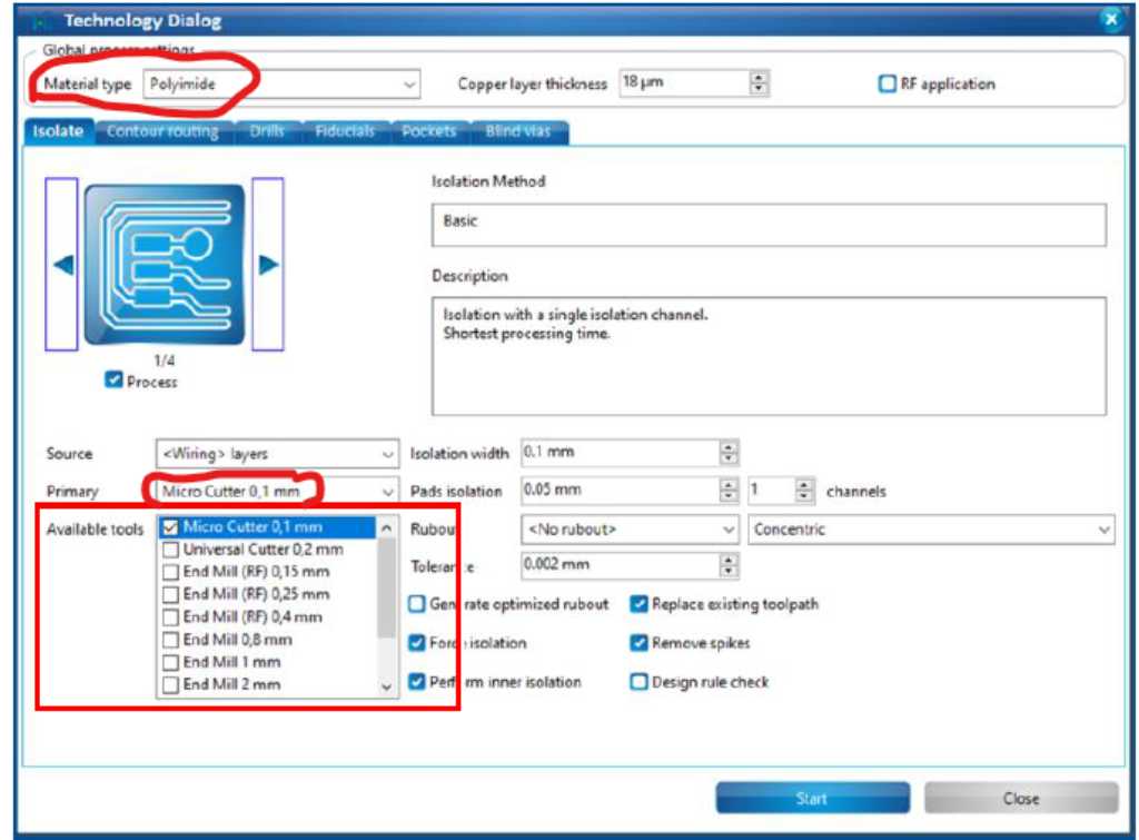
In the CircuitPro wizard I selected Polyamide as material and the 0.1mm microcutter as primary (and only available) tool, because according to LPKF tutorial, only this microcutter is capable of milling polyamide.
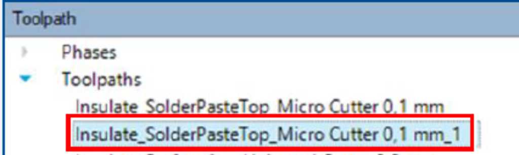
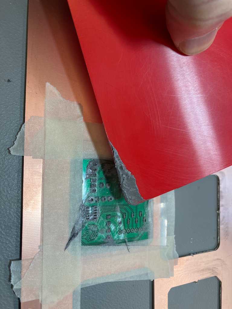
After creating these toolpaths, Circuitpro not only creates a toolpath to cut out the pads, but also toolpaths to fully mill them. This is not needed, so I’m deleting these:
The tricky part is the fabrication wizard. It asks for Copper thickness and Material thickness. As I’m not using any copper, but I want the sheet to be cut through, I add the sheet thickness as copper thickness. According to the LPKF manual, I should use 2.0mm (thickness of the drilling underlay plate) as material thickness.
Here is the big #fail. The mill happily mills just a little bit above the sheet. So nothing happened :-(. Apparently I should use a different value for the material thickness (thickness of the drilling underlay plate). Somewhere on page ‘too far down the manual’ I found that when you have a vacuum table, the material thickness should be set to 0mm. So I did and that worked perfectly!
The double sided tape I used was much to sticky so it was difficult to get it off, but eventually I got it and cleaned remaining glue with sticker remover.
soldering
Time to solder! Applying the solder paste:
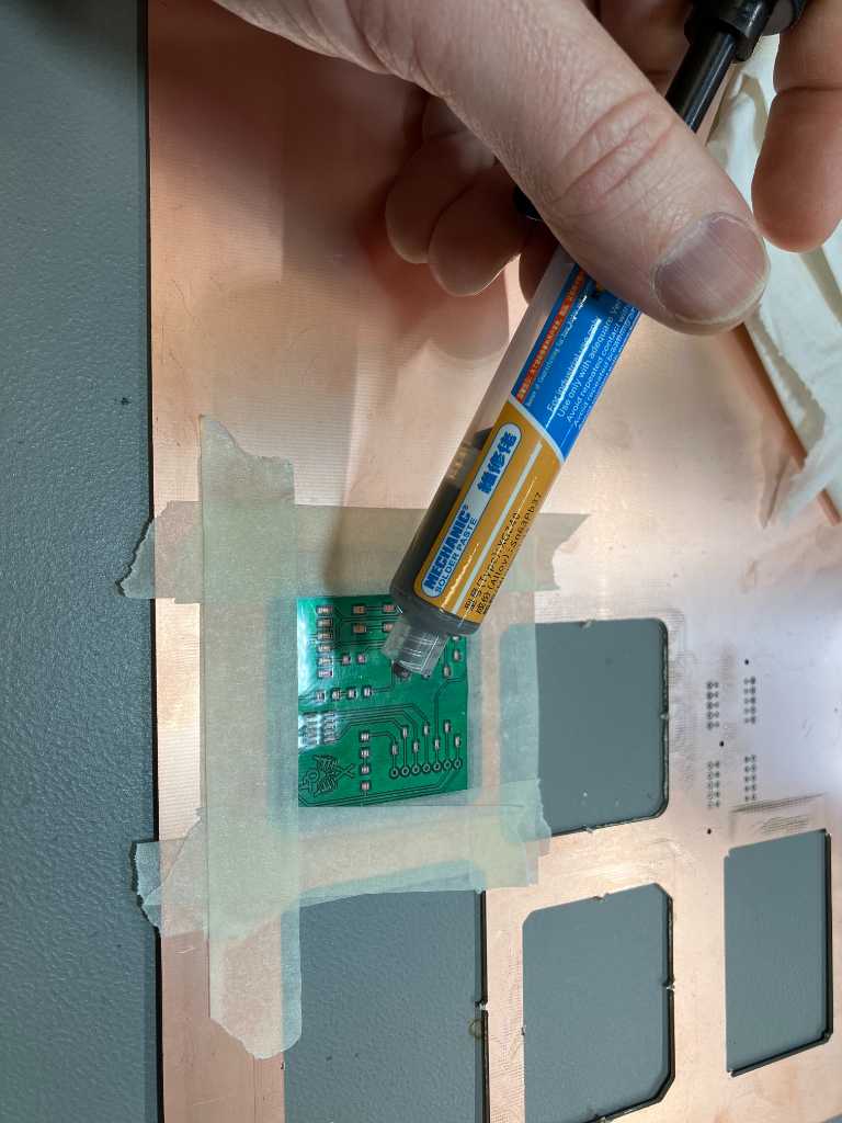
So that’s a really nice result. Maybe a bit too much solder paste to my taste, but I’m sure this will work out fine. By the way, the solder paste I use here is Mechanic XGZ40 solder paste with Sn63Pb37 tin/lead ratio.
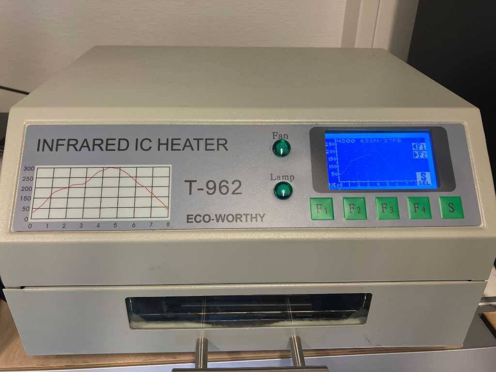
I actually first intended to do reflow soldering using our PCB oven. It’s a T-962 which is customized according to the well known tutorials online. Because it comes with painter-tape that holds the isolation inside. That gets really smelly, so when we got this unit I immediately swapped that for heat-resistant Kapton tape. I also added a temperature feedback sensor and uploaded a custom firmware that allows you to create custom heating profiles. One of the profiles is the 63Sn37Pb which is exactly what is needed for the solderpaste we have.
Although the oven works nice, I’m not sure if the headers that were supplied to us are resistant to reflow oven. So I decided to use our heatgun.
Most of the components are very straightforward how to place them, except for the LEDs. I always check because markings are all over the place. If manufacturers stick to the generally accepted rule, the kathode should be marked. However, we have a really neat component tester in our fablab and I gladly use this to find out the real polarity.
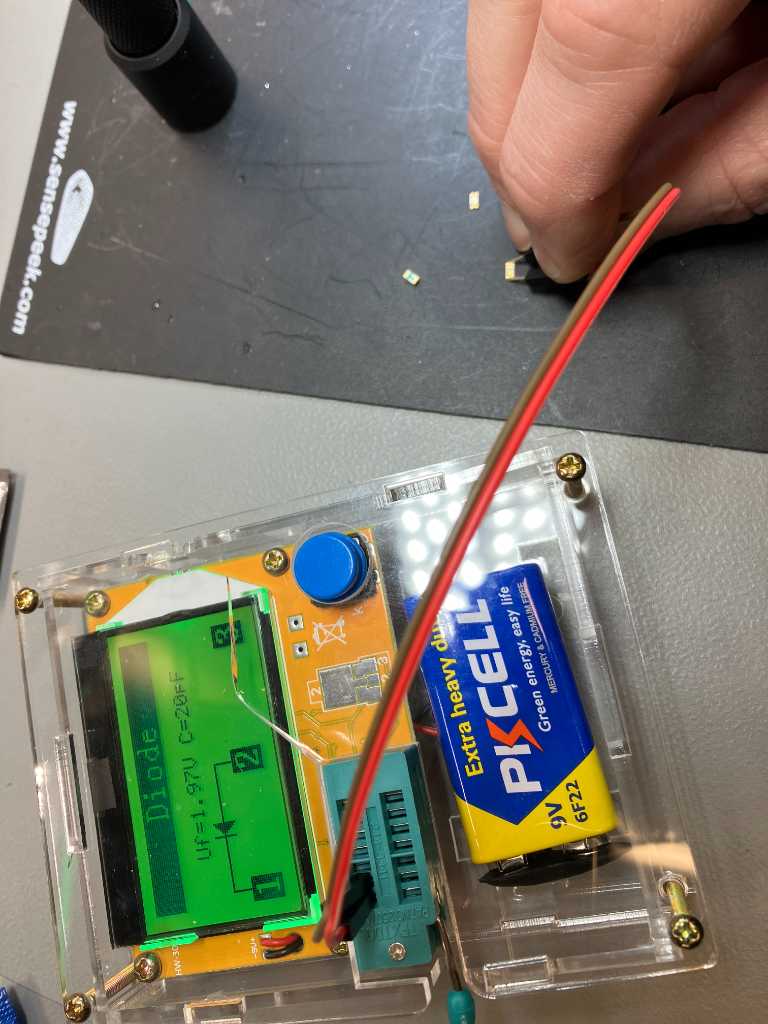
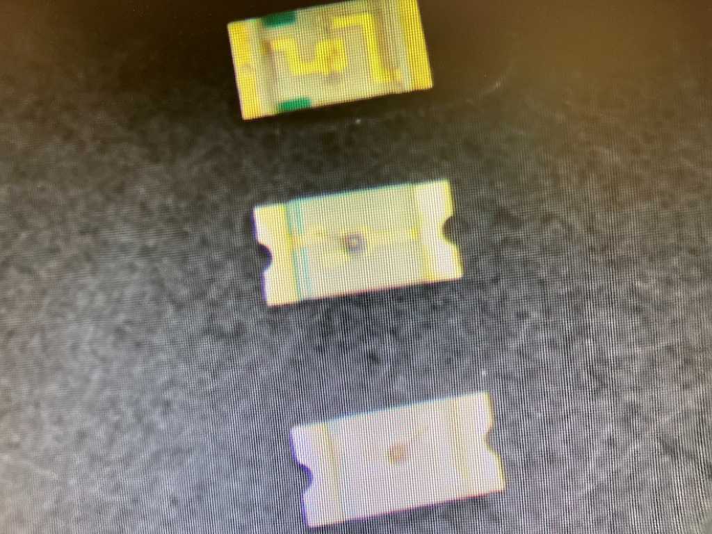
In this photo the LEDs are places with kathode to the left. From top to bottom: Blue LED, Red LED and Green LED. And yes, they all have different markings…
After carefully placing all components:
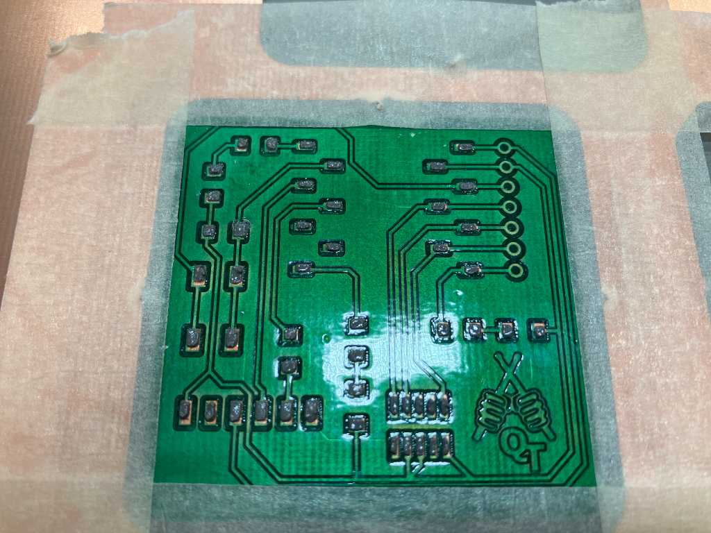
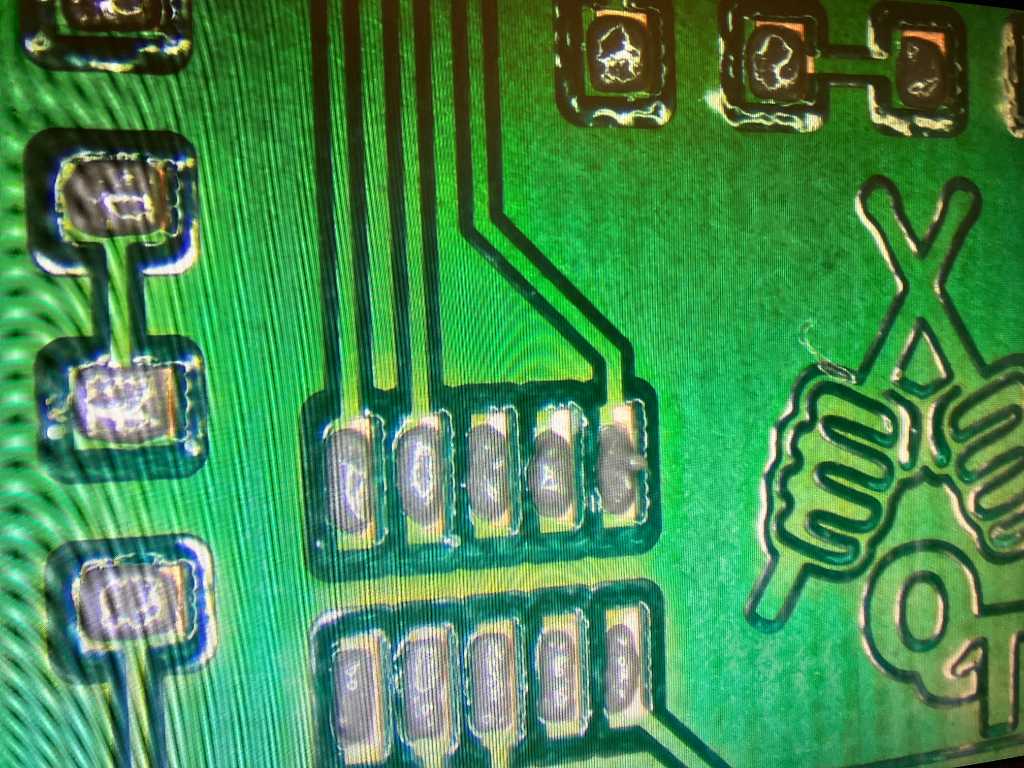
Time to solder:
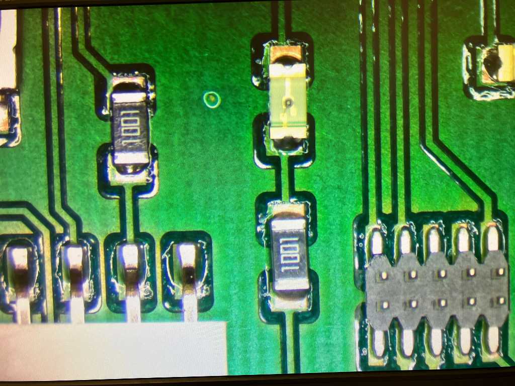
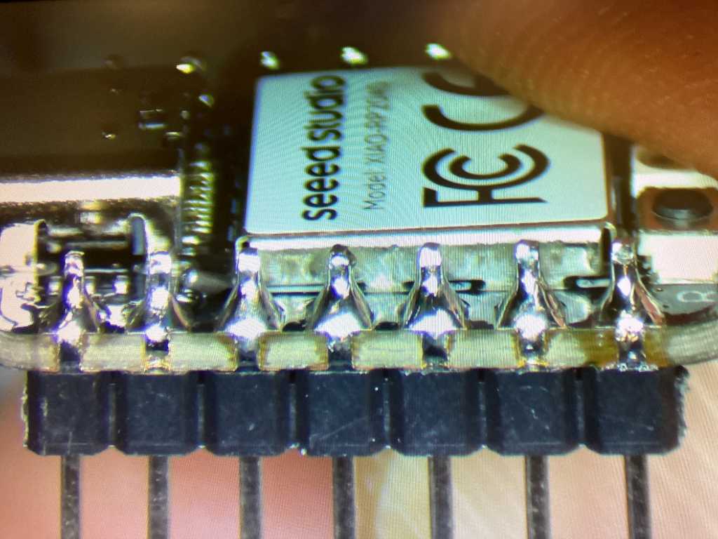
Nice! Here’s a microscope image:
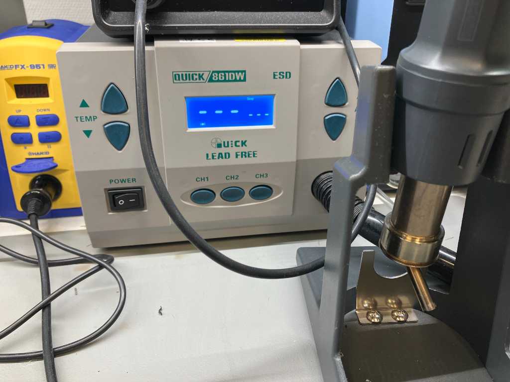
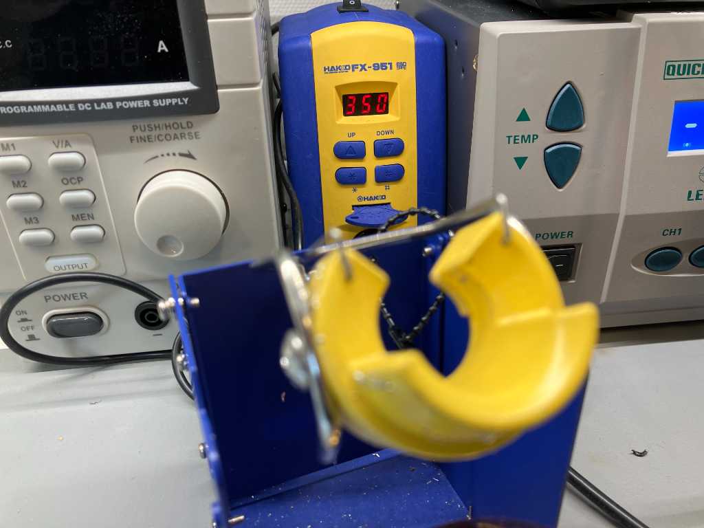
The through hole header pins of the Xiao should be hand soldered. I use our Hako for that.
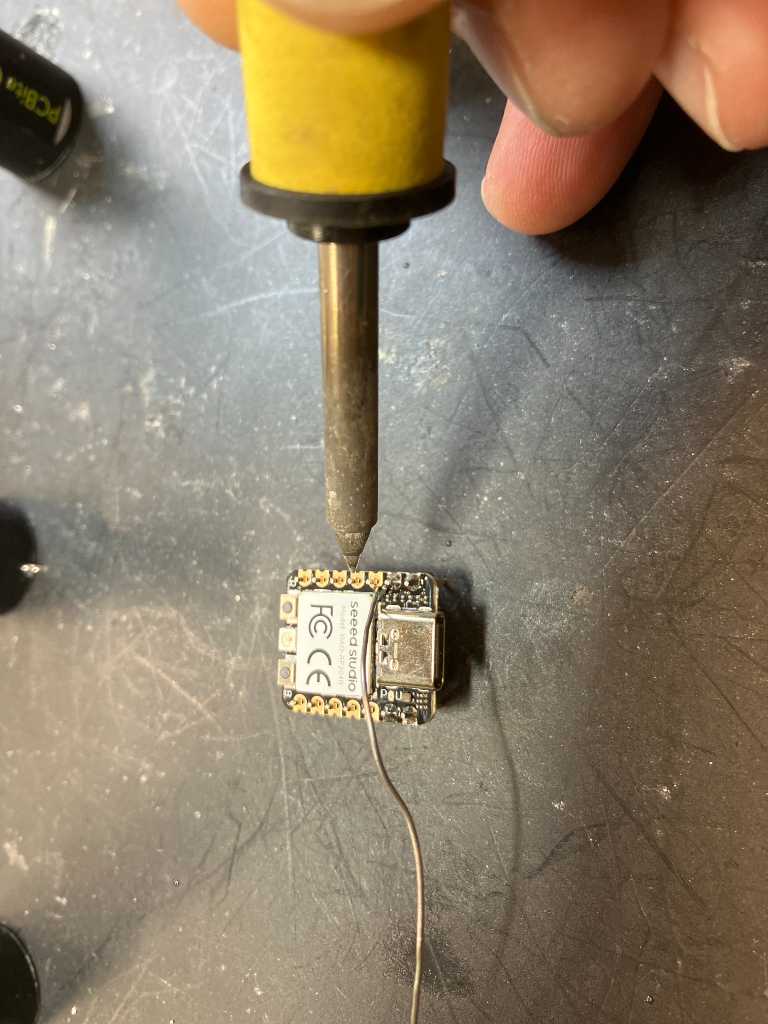
Nice :-)
And here’s the masterpiece:
programming: Blink it!
Now let’s find out if it actually works. For this I follow the guide of the quentorres repo.
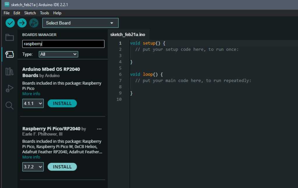
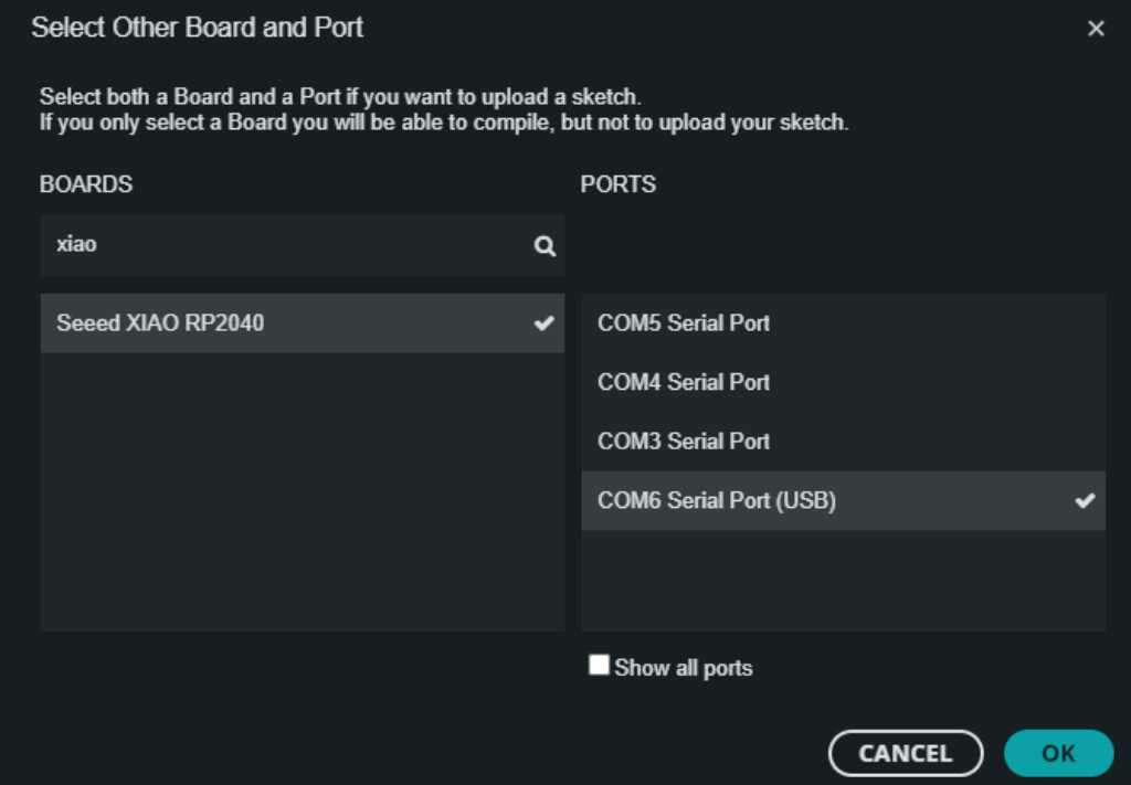
After adding the URL to the preferences of Arduino IDE, I could download the pico in the boardmanager:
I loaded the breathing LED example out of the Grove sketchbook that I once downloaded. Here’s the code:
// Demo for Grove - Starter V2.0
// Author: Loovee  2013-3-10
// Pulses the Grove - LED with a "breathing" effect.
// Connect the Grove - LED to the socket marked D3

// Defines the pin to which the LED is connected.
// Any pin that supports PWM can also be used:
// 3, 5, 6, 9, 10, 11

const int pinLed    = 26;

// Define the delay for the "breathing" effect; change this
// to a smaller value for a faster effect, larger for slower.

const int BREATH_DELAY = 5; // milliseconds

void setup()
{
    // Configure the LED's pin for output signals.
    pinMode(pinLed, OUTPUT);
}

void loop()
{
    for(int i=0; i<256; i++)
    {
        analogWrite(pinLed, i);
        delay(BREATH_DELAY);
    }
    delay(100);
    for(int i=254; i>=0; i--)
    {
        analogWrite(pinLed, i);
        delay(BREATH_DELAY);
    }
    delay(500);
}
And it works :-)
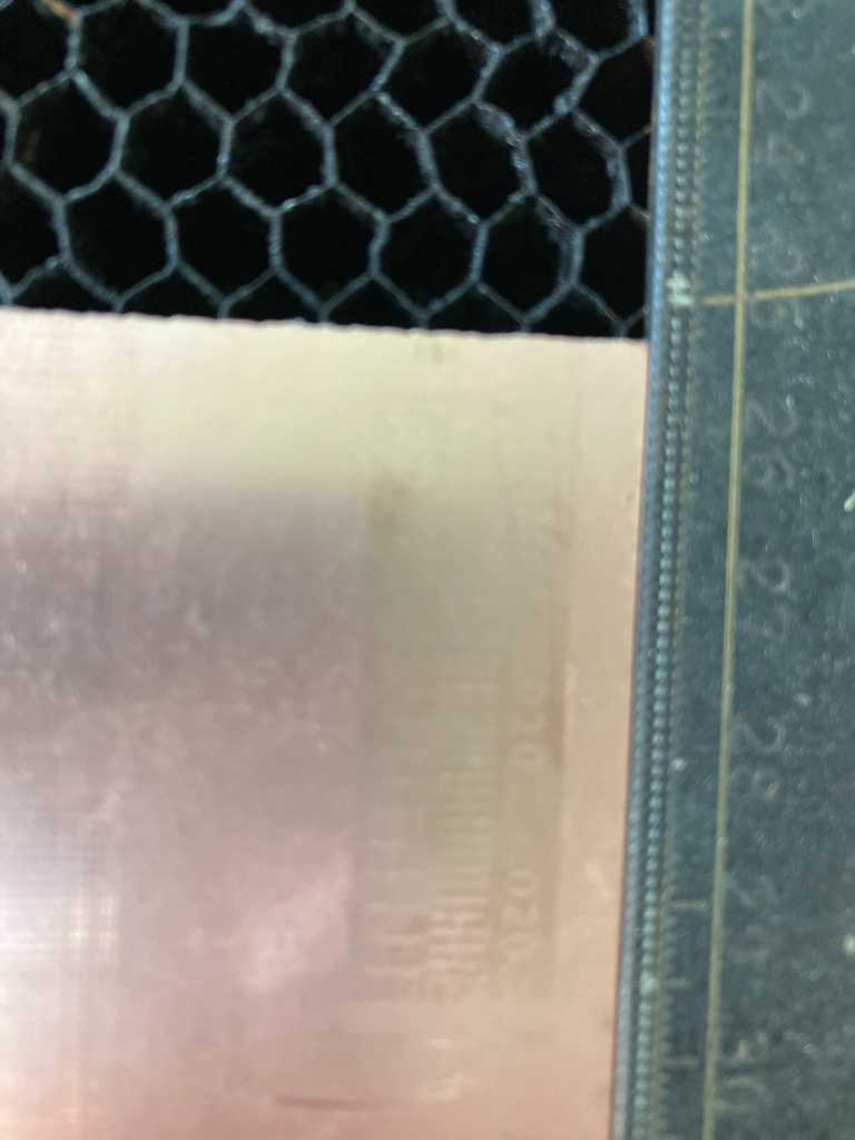
Fiber laser PCB production
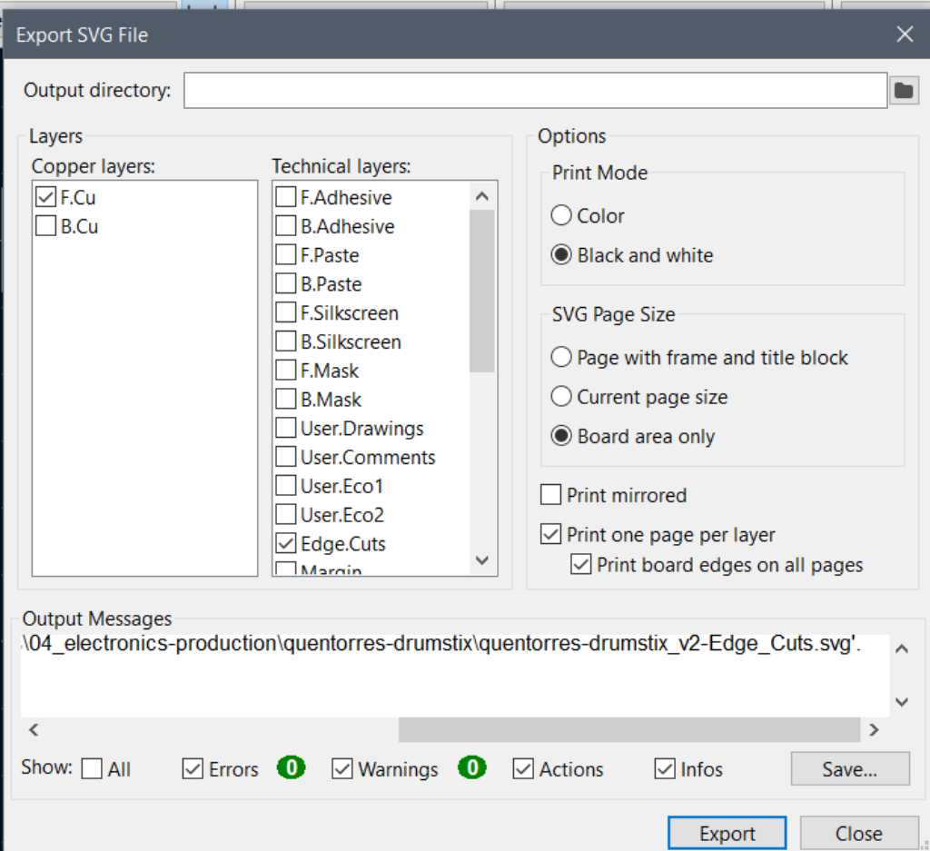
I want to try to produce a PCB using our Trotec Speedy 300 Flexx (which has a 20W FLP source). For this I need to export the Quentorres design as SVG file. This was easily done in KiCad using File - Export - SVG.
But before making this programmer, I will first do the traces test.
So I loaded the traces.png file into Trotec Ruby software and set power to 100%, speed to 0.4% and source to FLP. After 15 minutes on 20W FLP with power 100% and speed 0.4% this is the result:
The LPKF would already be done now… This is quite strange. It hardly cuts through the copper layer. I tried engraving a 5x5mm square at speed 0.1% and it didn’t produce any usable result either. So either the 20W FLP is not strong enough, or the lasertube doesn’t produce 20W anymore. I searched various fabacademy websites of people who were able to do this on their fiber, like here at opendot in Milan and here at MIT. But I wasn’t able to do this myself, I call this a #fail. We will have a mechanic look at our Trotec lasercutter and let him do some maintenance and measure the lasertube. Hopefully after that I’ll work.
creating vias
There are several ways to create vias. I can think of the following:
- Electroplating (adding copper using a chemical reaction, mainstream in PCB productionhouses)
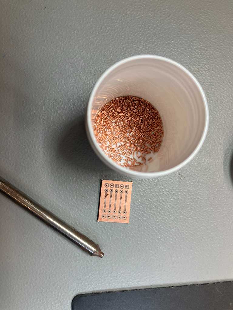
- Copper rivets, manually added with a stamp tip (we have 0.7mm rivets at the fablab) and then soldered
- Fill the via with conductive epoxy (usually silver based, chemical-alert)
- Fill the via with a piece of copper wire and solder on both sides (never tried, but that will be ugly I think)
- Fill the via with solder wire and melt it
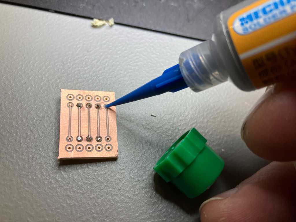
- Fill the via with solder paste and reflow solder
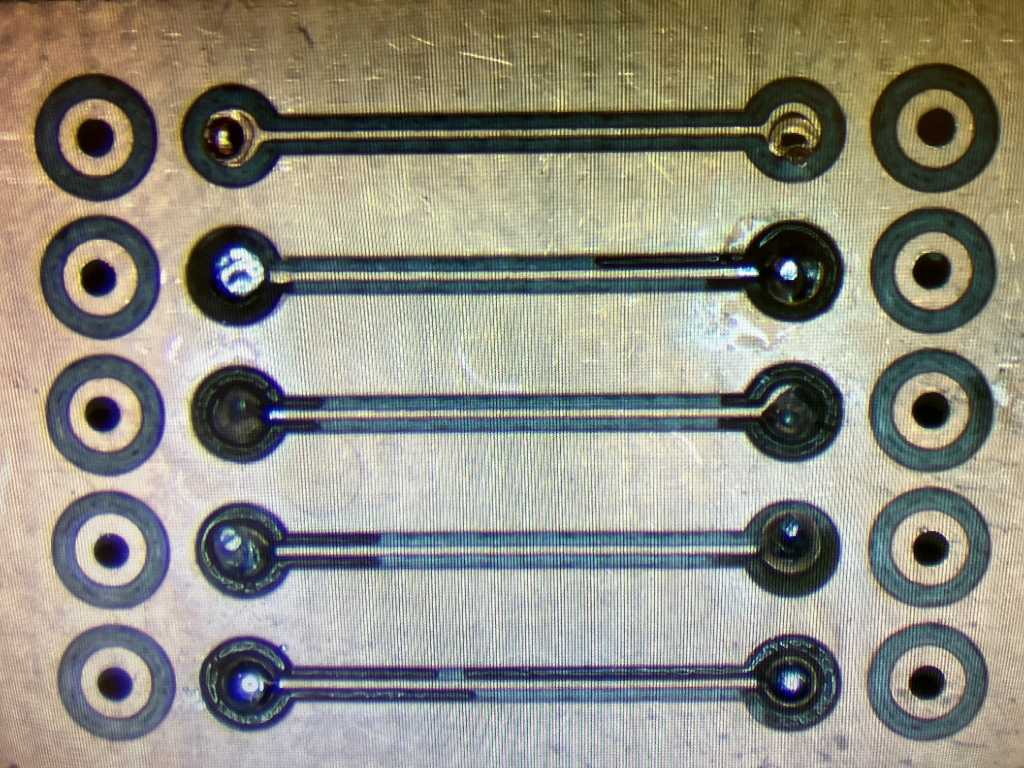
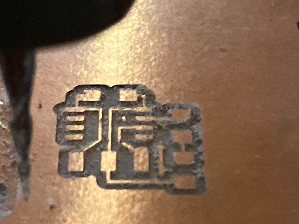
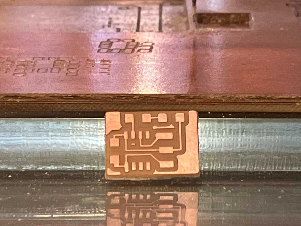
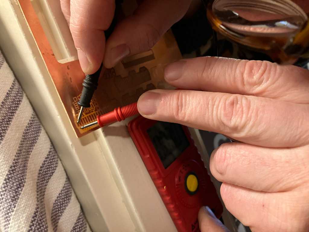
So far I’ve only used the rivets. We strive to use as little chemicals as possible in the fablab. But would be cool to test if any of the other options work. To try, I created this test PCB:
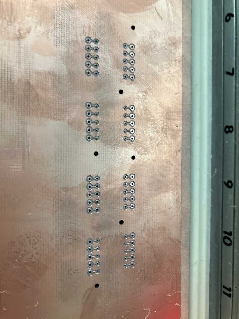
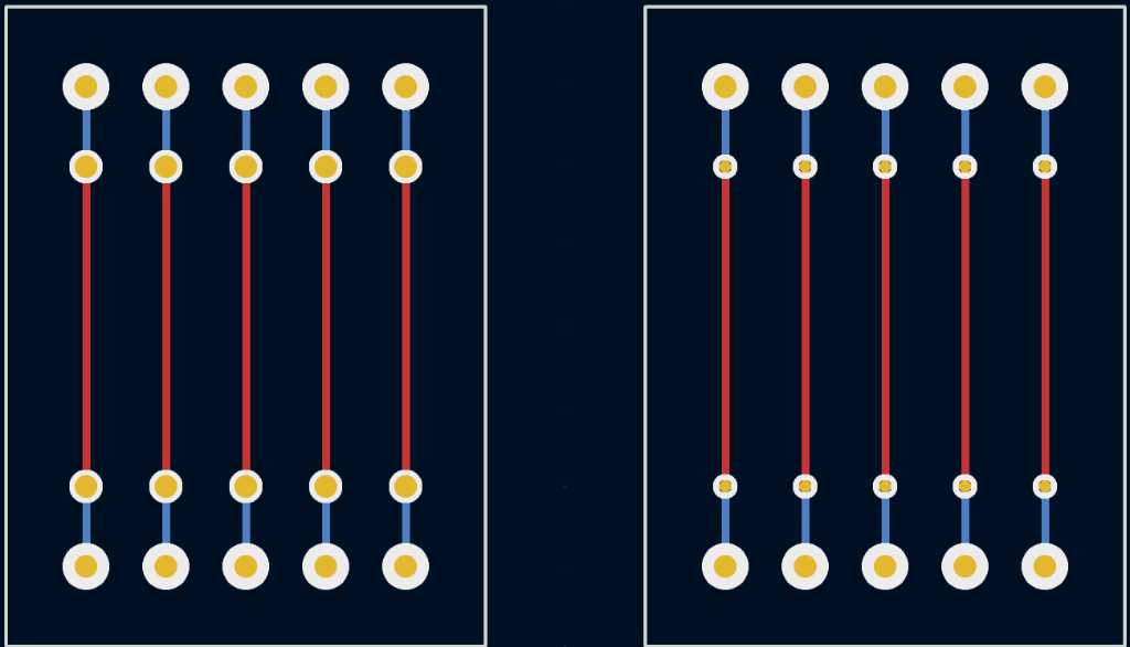
Rivets:
Solder wire through the via:
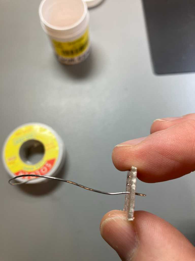
Copper wire through the via:
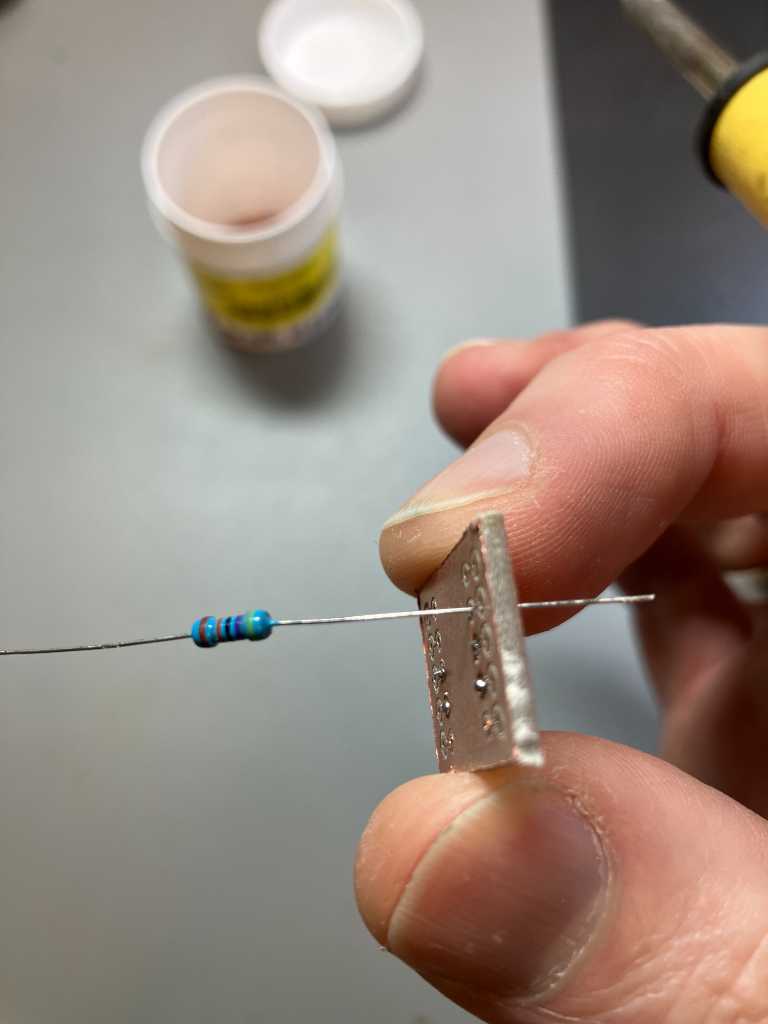
Solder paste through the via (soldered using hot air gun):
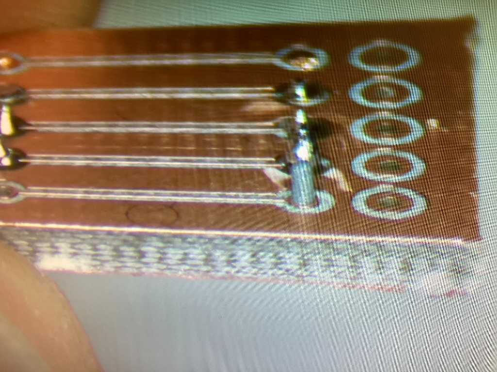
The result:
- rivets -> measures 0.2 Ohm
- rivets with solder -> measures 0.0 Ohm
- solder wire -> not conductive
- copper wire soldered -> measures 0.0 Ohm
- solder paste -> not conductive
So to conclude: making the via using rivets is doable, but takes care and time. You can see that soldering it afterwards is actually a good thing both for a stable connection as well as increase conductivity. Doing it with copper wire is not easy at all because you first have to solder one side, then the other and hope the first one will stay intact, then cut wire.
Creating vias using either solderwire or solder paste is a bad idea. They are both non-conductive and there’s no way to tell.
Link to repo
What I learned this week
Successes
Kicad: I have to say that changing the board, getting the svg logo (creating a foorprint) on it and exporting it for fabrication was a fairly simple and straightforward process. So far I like the simplicity of kicad. The thing I didn’t like is that when moving devices, the connected traces don’t move with it. This is something Altium and Fusion360 do.
I was able to make vias using quite some methods. Using copper rivets and soldering them afterwards is most preferably.
Fails & Fixes
No unexplainable fails this week. Blunt mills, wrong settings, and not paying attention :-)
So easy fixes: Swap for new ones and check doublecheck triplecheck.
Unfortunately the fiber laser production didn’t work out. I hope to try it again after the maintenance has been done.
Remember this for next time
KiCad PCB editor is very straightforward. Making PCBs is fun, but takes time.