Week 8: Electronics design
Assignment
Group assignment:
- Use the test equipment in your lab to observe the operation of a microcontroller circuit board
- Send a PCB out to a board house
-> It can be found on our fablab web page.
Individual assignment: - Use an EDA tool to design a development board to interact and communicate with an embedded microcontroller, produce it, and test it
What I did
I designed a PCB that I will use for my final project!
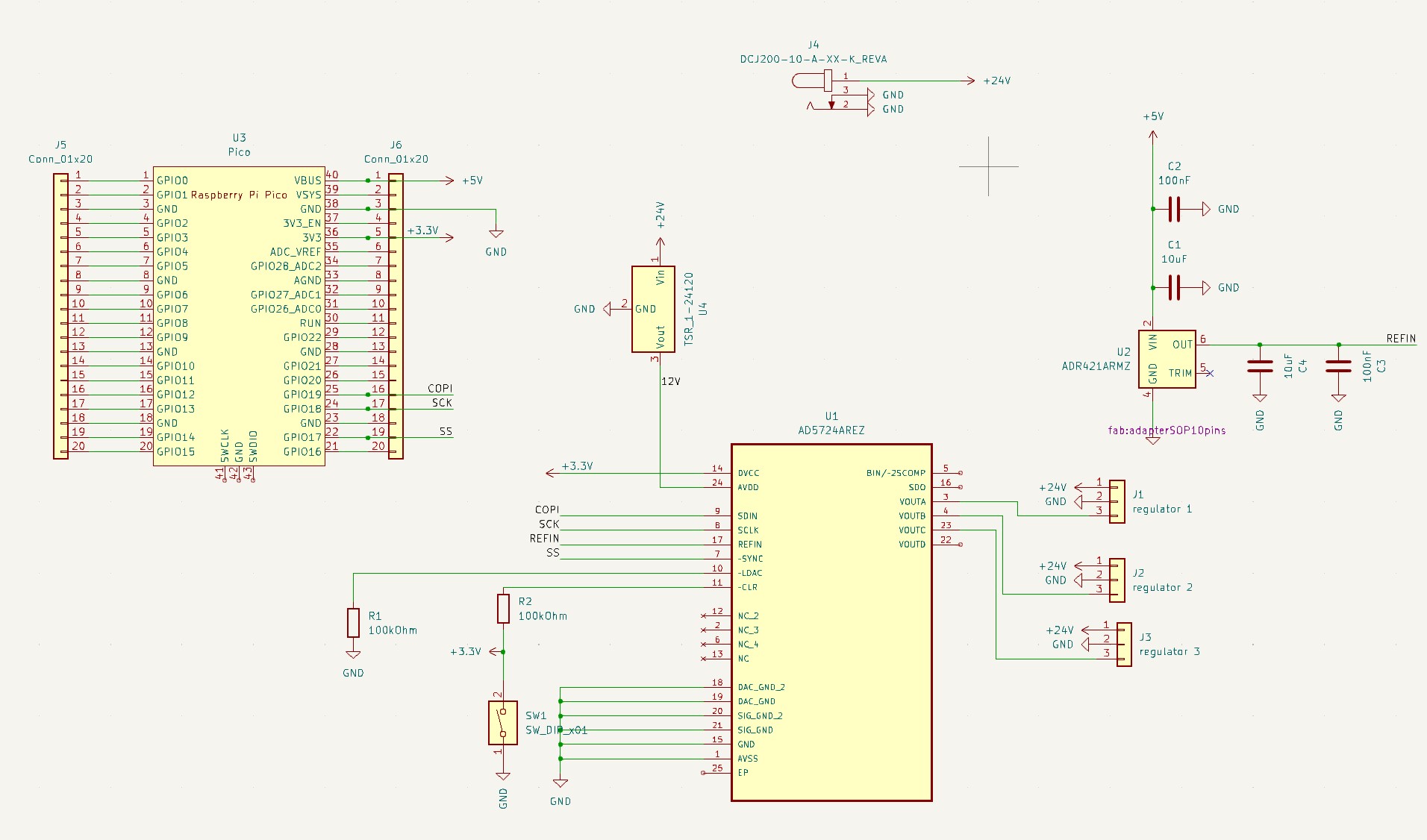
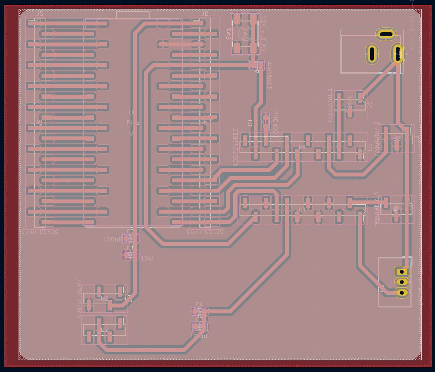

PCB for pressure regulators control
Purpose of my PCB
For this week assignment I designed a PCB that I will use for my final project (see pressure control here): the goal is to being able to control pressure regulators (Festo VPPE) by using analog signals ranging from 0 to 10V. To do so, I designed a PCB that integrates a RP2040 pi pico microcontroller and a DAC (digital-to-analog converter) that will convert the command to a analog signal to send it to the pressure regulators and obtain the desired output pressure.
RP2040 microcontroller choice: I chose this microcontroller for multiple reasons: available at my fablab, it allow the SPI communication to interact with the DAC, and it has a lot of GPIO that will be usefull for the different sensors and pump that I will need to connect to my microcontroller.
DAC choice: It was based on my requirements for the control of the pressure regulator: I need to control 3 pressure regulators independently (i.e. send different signal control to have different output pressure in each channel), the pressure regulators are commanded by analog signals ranging from 0-10V. The DAC I chose has:
- 4-channels output
- selectable output range, including 0 to 10V
- serial communication via SPI to communicate with my RP2040.
Design of the PCB
I used the DAC datasheet and the RP2040 datasheet to know how to connect my DAC and my microcontroller. I need to identify the pin that must be connected together between the DAC and the microcontroller, as well as the different supply voltage needed.
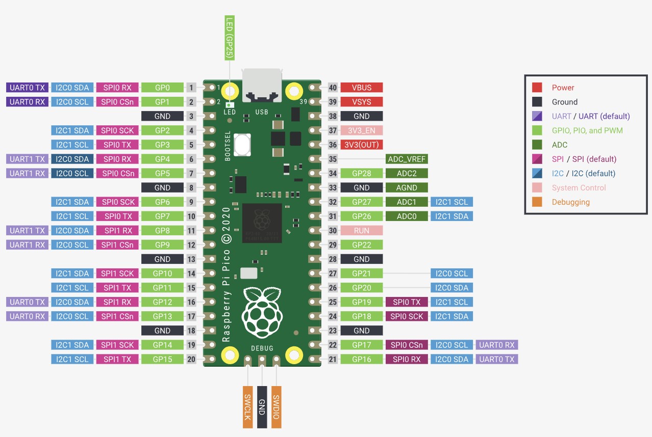
I identified the SPI pin of the microcontroller, that will be connected to the DAC for the communication bewteen the two. Note that:
- SS/CS: 2 notations for the same thing: slave select/chip select
- here the notation RX/TX is used instead of the classical COPI/CIPO ➔ CIPO stands for Controller Input, Peripherical Output.
COPI stands for Controller Output, Peripherical Input. As data is received (RX) on the input and data is sent (transmitted, TX) on the output, from the master’s point of view, CIPO is its RX pin and COPI is its TX pin, so:
CIPO = SPI_RXD
COPI = SPI_TXD
Based on the datasheet reading, I add some components to the design of my PCB:
- A precision voltage reference (ADR421), which is the recommended chip to use as the external reference voltage input
- Some pull-up/down resistors to ensure that a wire is pulled to a high/low logical level in the absence of an input signal -> for example, the connection of the LDAC pin of the DAC will be connected to a pull-down resistor to keep this pin permanently low
- Decoupling capacitors
I also need a 24V DC supply voltage for the pressure regulator, so I add a DC jack connector on the PCB. I will used also this 24V supply voltage and a regulator to obtain a 12V input voltage for my DAC (it requires a input voltage between 10,9V to 16,5V based on the datasheet). Note that the DC jack connector available that I had is a through hole component, but I will use a one layer PCB, meaning that I will put the jack connector under my board so the pins can be solder on the copper side of my board -> I need to invert the footprint on my PCB design. The same trick will be done for the regulator.
I did a hand schematic before starting the design with an EDA tool.
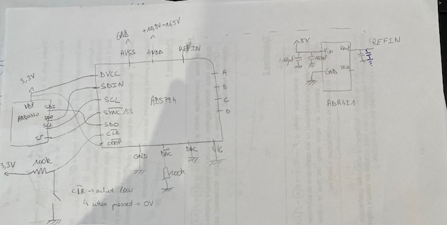
Designing my PCB with KiCad
I used KiCad 8.0 to create my PCB, here is the different steps that I followed:
Schematic
- Create a new project ➔ first thing is to create the schematic of the circuit ➔ schematic editor
On the schematic, all the components of the PCB will be added, as well as the connections between them and the supply voltage/ground. To add a component, it’s done as follow:
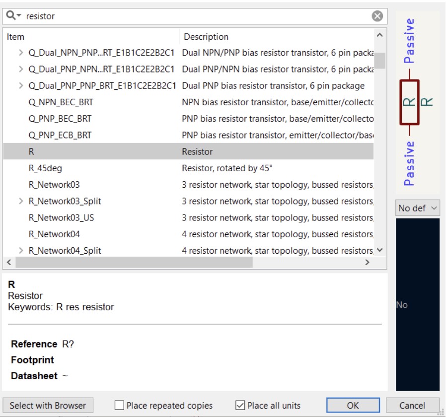
- Add a symbol ➔ ex: resistor ➔ ok ➔ place it where you want on the schematic
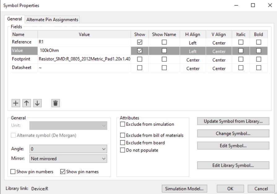
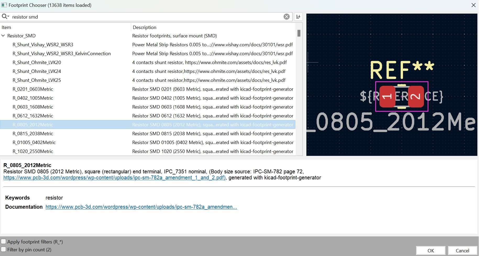
- Add a value and a footprint to the component. The footprints define the copper connections between physical components and the routed traces on a circuit board, it’s thus important to choose the good one corresponding to our components. Important to associate a footprint to the component so the footprint will be added directly to the PCB design file when I will create the PCB from the schematic. To do it: zoom on component ➔ change the properties: Value and footprint ➔ select what needed. I choose the standard R_0805 for the footprint of the resistor because I have this resistor available in my fablab and the size is ok to solder it.
-
Add the other components in the same way
-
Components not available: The existing libraries in KiCad obviously don’t include all the electrical components, you must sometimes create your own library that will have the symbol and footprint that you need for your project. For example, the DAC component that I’m using was not directly available on Kicad ➔ I went on SnapMagic and downloaded the Symbol and Footprint file for KiCad. Then I followed the tutorial to import new library on KiCad. Now it’s available and I can import it on my schematic.
-
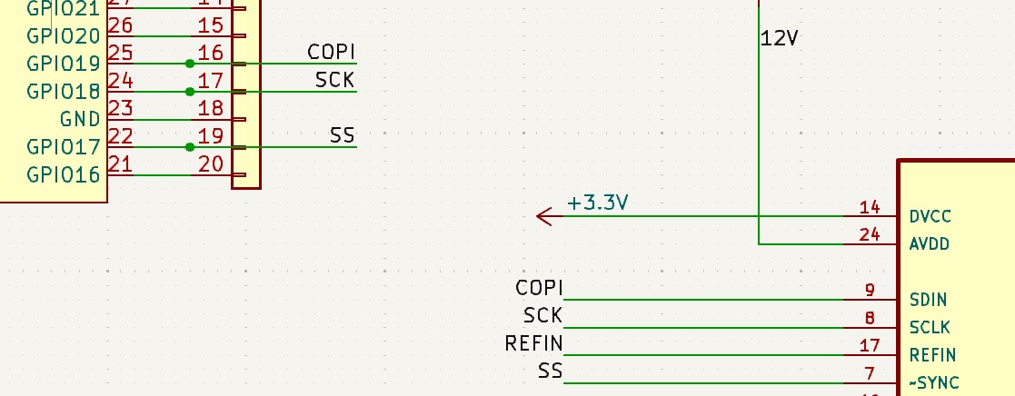
When all the components are added in the schematic, it’s time to link them between each other. I used the hand schematic that I did before to help me, and I also used some labels to connect pins to each other without having a messy schematic (as the handmade one). For example, you can see below that I connected the SPI pin of the microcontroller and the DAC by using labels to have a clear view of what is linked.
- Usefull connectors: In order to be able to connect input and output devices to my microcontroller, I added connectors linked to each pin of the microcontroller, as shown below.
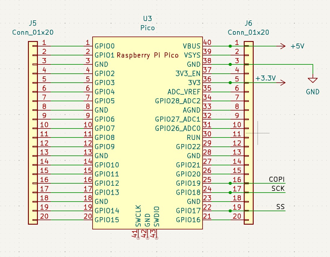
Final schematic

The KiCad file can be downloaded here, and the PDF file here.
PCB
When the schematic design is ready, the PCB can be updated directly based on the schematic: tools -> update the PCB from schematic (or F8). It will import all the footprint preselected and will show the connections between the different components (called ratsnest).
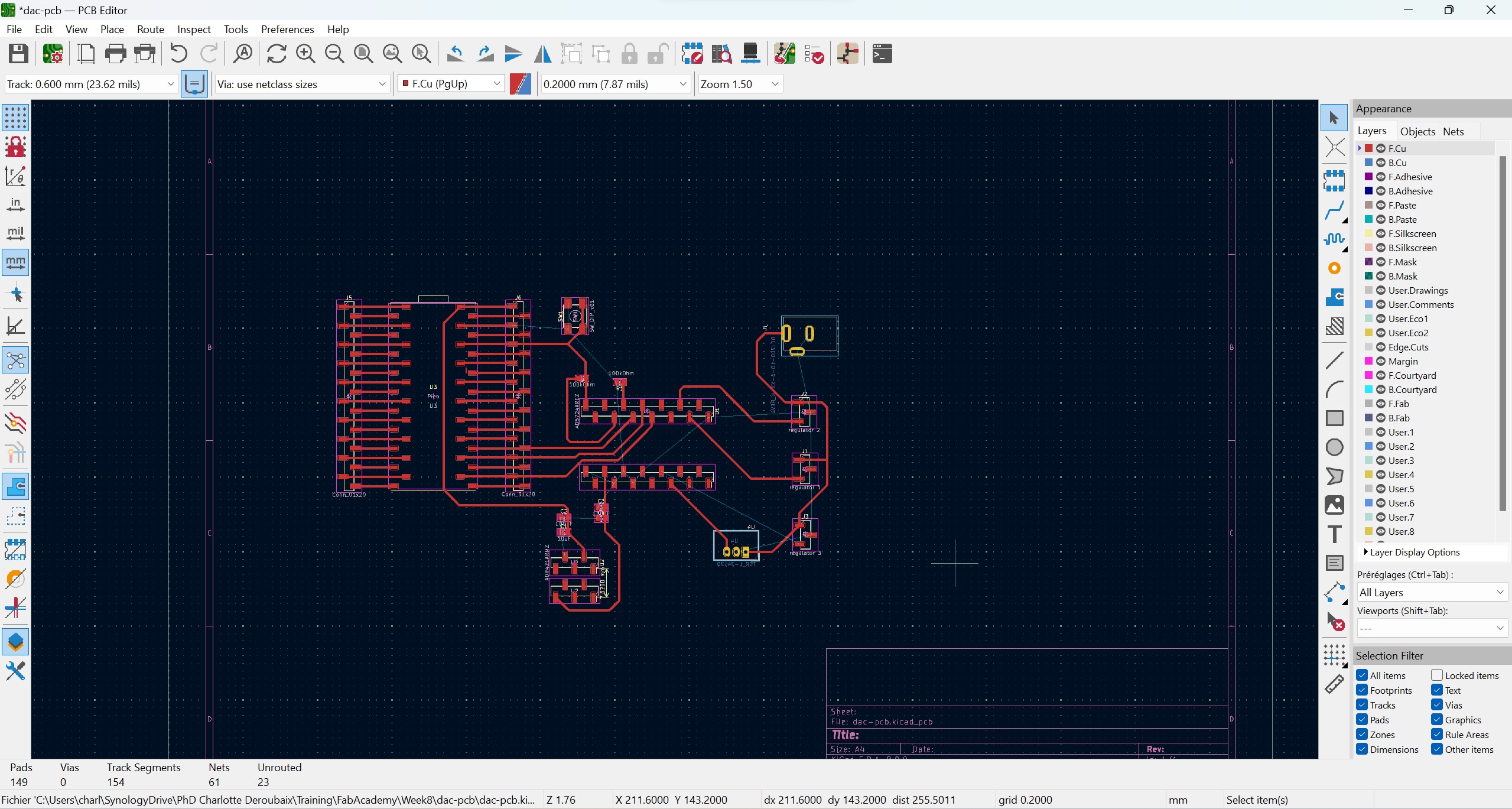
- Now the “fun” part begin to connect every pin with traces, without crossing them.
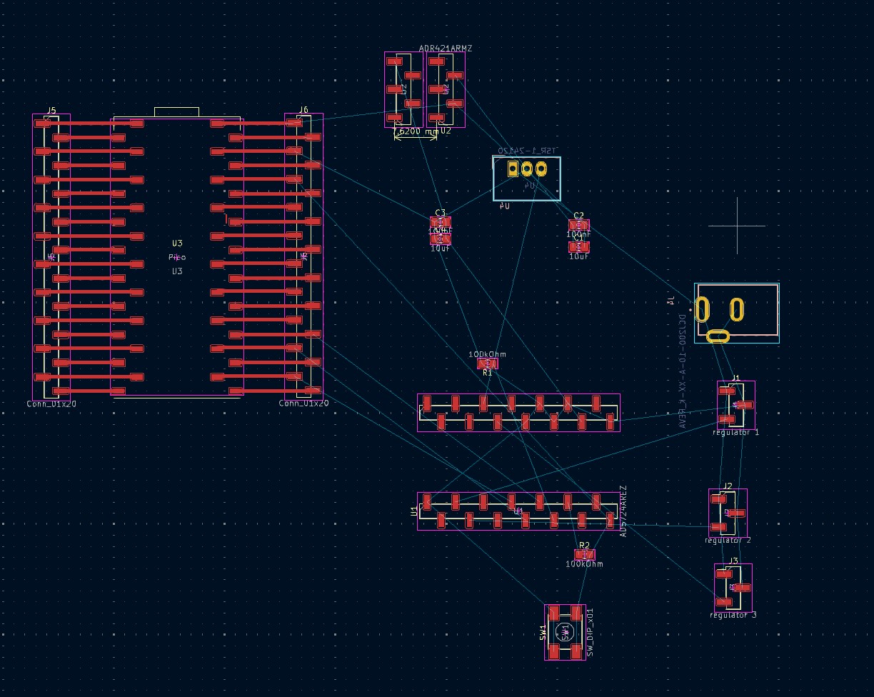
-
Traces: In the board custom window you can add pre defined size for the traces, meaning that all the traces that you do will have the selected dimensions. It can be usefull in order to select traces not to thin in order to be sure that the milling process will be done correctly, and also to facilitate the soldering process. Here I selected traces of 1mm.
-
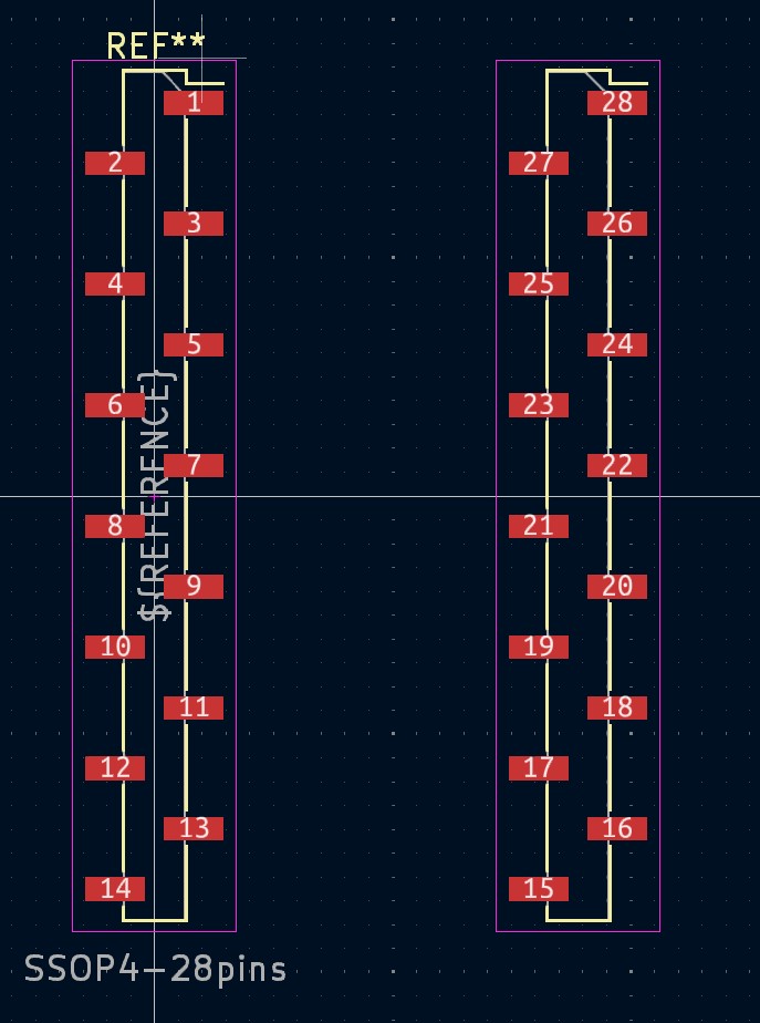
Footprint changes when doing my connections, I realised that the DAC component and the voltage reference chip have very small connector, that would have lead to super small traces (0,25mm), so I decided to use adapters shown below. The adapters will allow to have bigger traces because I will solder the component on the adapters and plug the adapter on the board. Moreover, if I want to change the design of my board at some point, I will be able to reuse the same DAC and voltage reference chip and plug them directly on the new board -> cost saving.
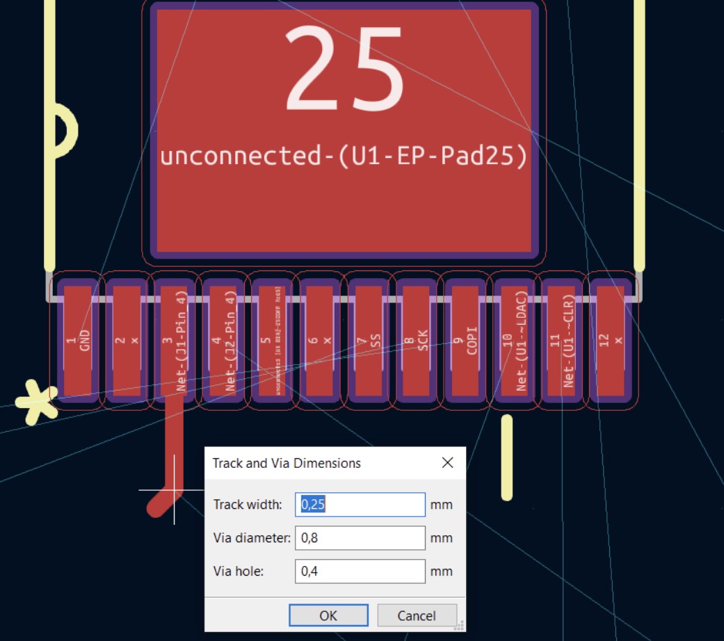
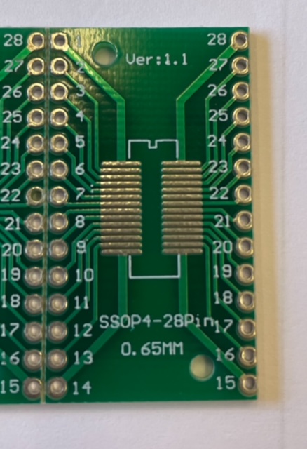
I didn’t find available footprint library for that kind of connector so I created it myself by using existing components.
- Creation of a footprint: on the PCB editor -> “create,edit and delete footprint” -> “create a new empty footprint” -> enter a name -> draw your footprint or use existing components to start your footprint. I used one existing connector with the good dimensions that I copy pasted and I just spaced them with the good dimensions as well (15.24mm for the DAC and 7,62 mm for the voltage reference chip).
- Here is the result when all pins have been linked
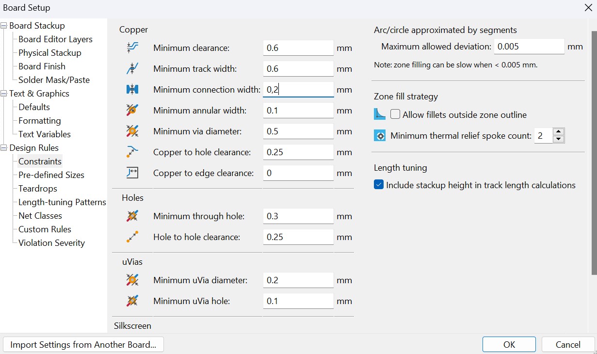
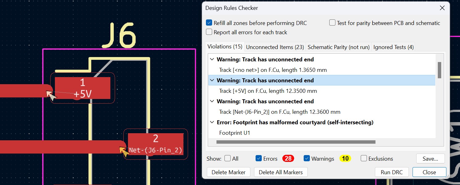
- Almost finish: now I want to check if the design rules are all checked -> there is a check list button on the PCB window that will allow to run a “Design Rules Check” (DRC). Before doing it, I added some constraints in the setup board window, to be sure that the clearance and track sizes are respected. It will be checked during the DRC.
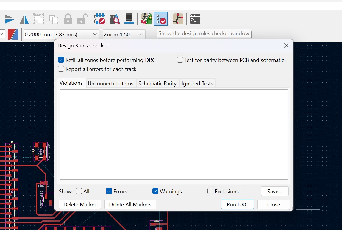
Example of design checking: it will show all the error and warning to finish the PCB design.
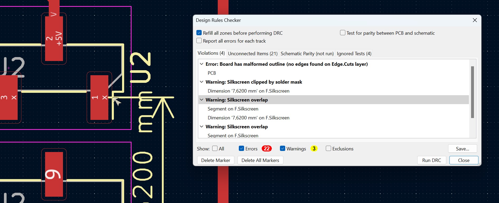
- Other warning issue due to a bad manipulation when creating my footprint: need to go in the footprint file to edit it derictly from there and have a clean library.
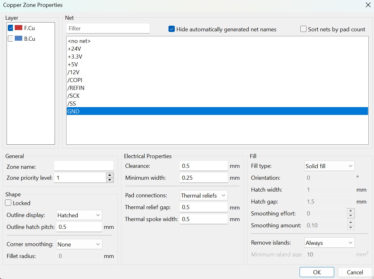
- Creating the GND zone: when the DRC is done and everything is corrected, the ground zone can be created. To do so: add a filled zone -> click where you want to start the zone -> select RED = GND -> ok -> draw the zone -> select the zone -> right click -> zone -> fill the selected zone
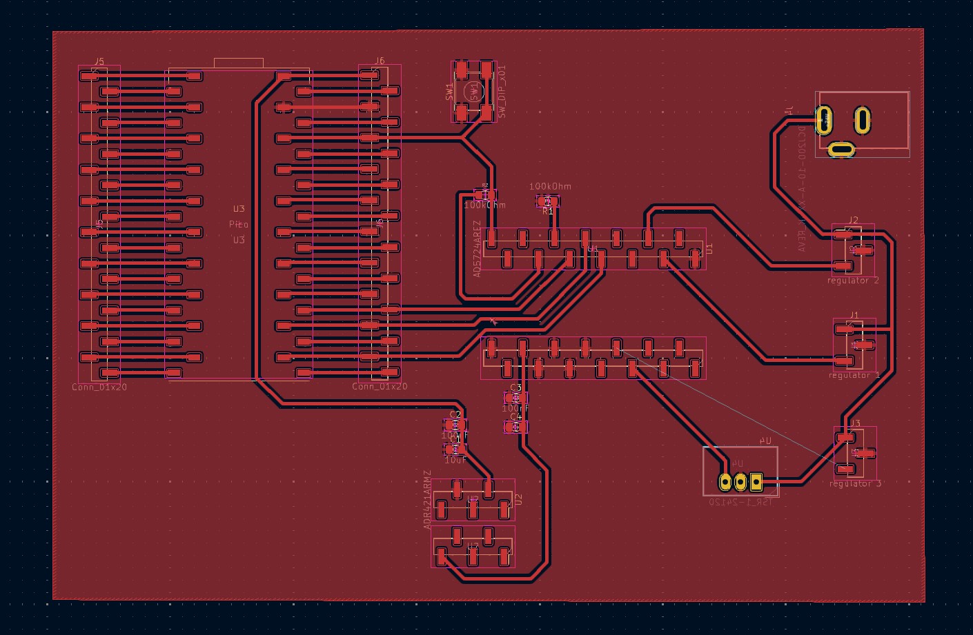
- Check that there is thermal relieves around the ground pads to help soldering:

- Last step: select the “edge.cuts” layer and add a new zone as before -> it will be used to cut all around your PCB.
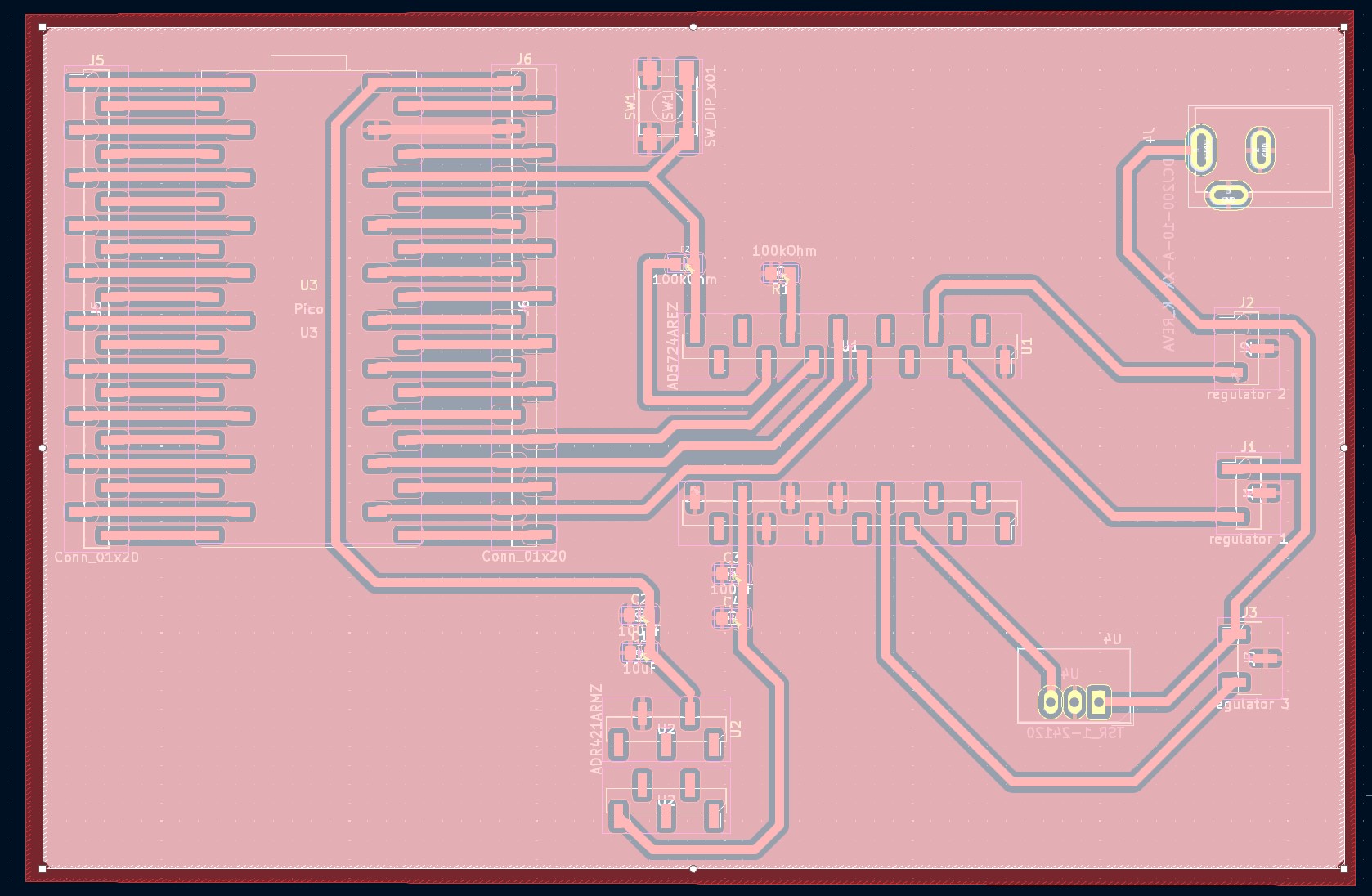
Final PCB
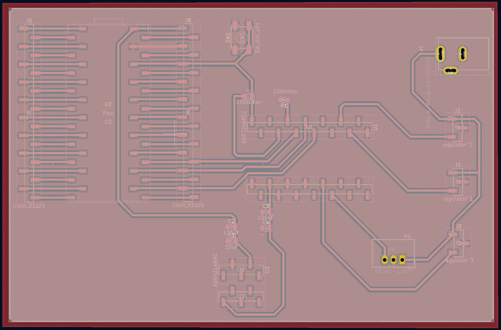
The KiCad PCB file can be downloaded here
PCB errors and modifications
-
I did a very dumb mistake when designing the footprint adapters: I didn’t have adapters with the good number of pins so I took larger adapters i.e. 28pins instead of 24 for the DAC and 10 instead of 8 pins for the voltage reference chip. But I should have designed the footprints for 24 pins and 8 pins, which I didn’t so all my pins connection were shifted.. I updated the footprints for 24 pins and 8 pins, and I did the traces again.
-
I compacted everything on the PCB: first version that I did was 14cm long, which is too much for the Bantam -> I reduced it.
-> Final version of the PCB

Milling
Creating the gerber file on KiCad
To create the gerber files that will be used for milling the PCB with the Bantam tools:
On the PCB file: file -> fabrication outputs -> gerbers -> select the zone that you want to export -> plot : it will create a “F_Cu.gbr” file for all the traces/footprints and a “edge_cuts.gbr” for the exterior cutting.
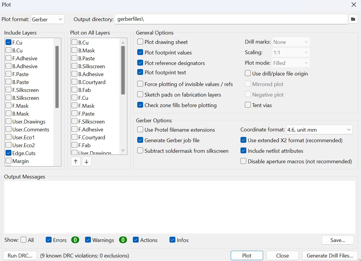
For the drills: click on generate drill files.
-> ready for the milling
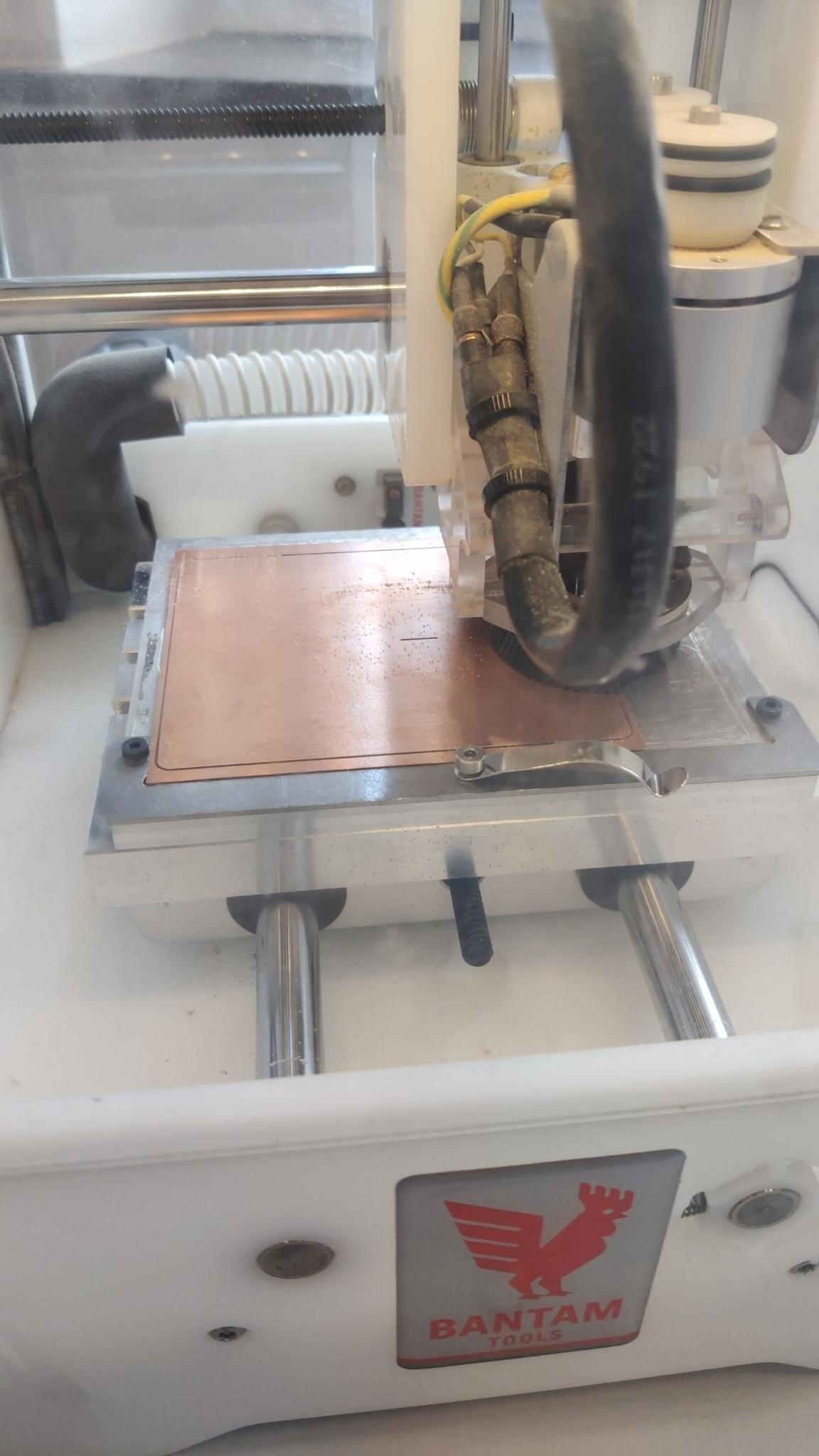
Soldering
For the soldering, I used the super magnifying glass of my lab, which helps a lot for the very small components that I had to solder.
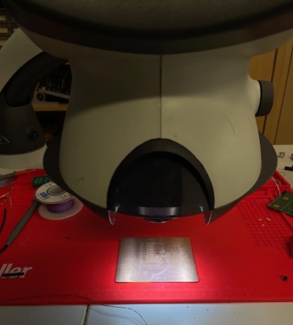
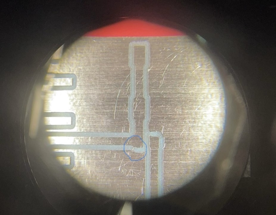
The magnifying glass also helped to check the imperfection of the PCB engraving: some parts of the copper were not completely removed as the one shown on the example below. I used the tip of a screwer to remove it completely, rather than a cutter because I wanted to remove everything and the cutter is a bit to thin.
I started with the smallest components and soldered them on the adapter, before soldering the header as well on the components. Than i soldered all the components on the board: resistor, capacitor and button. I finished with all the different header.
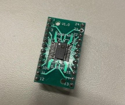
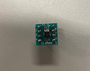
Soldering process
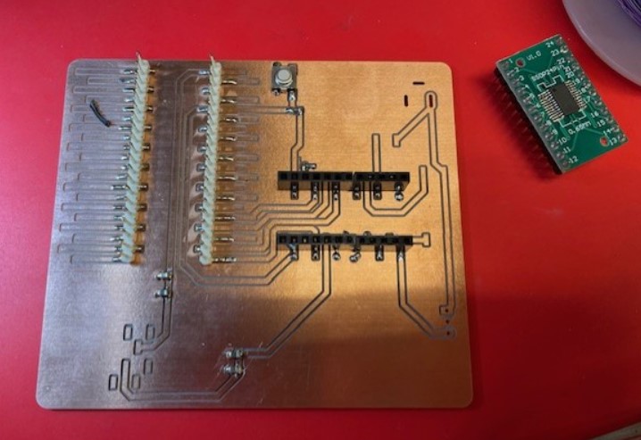
Final board after soldering
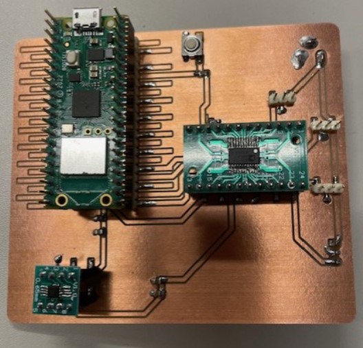
Testing my board
Multimeter testing
I first checked all my soldering with a multimeter, for example I was a bit afraid that these connections was touching the ground plane.
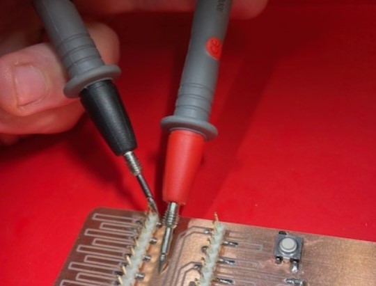
All my soldering looks fine with the multimeter, no short-curt were found during the checking, nor open circuits.
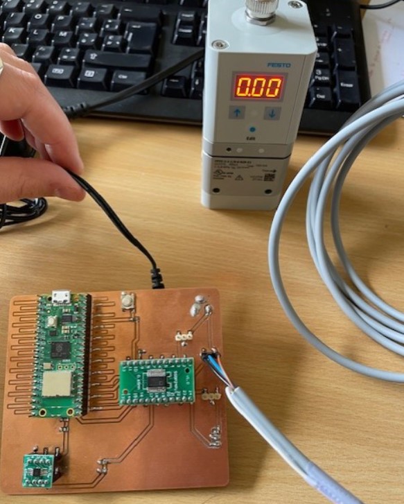
Switching on the pressure regulators
Before trying the communication between the microcontroller and the DAC to send the desired analogic voltage commands to the pressure regulators, I just tested if I was able to switch on the pressure regulators with my board. I connected the pressure regulators on the board and I connected the 24V DC supplier with the jack -> it works, the pressure regulator is working!
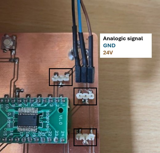
Testing the microcontroller
I tested the microcontroller with a LED: working!