Week 14: Networking and communication
Assignment
Individual assignment:
- Design, build, and connect wired or wireless node(s) with network or bus addresses and local input &/or output device(s)
Group assignment:
Send a message between two projects -> see group page
What I did
I didn’t really know what to do this week, as I had already tested I2C communication during week 12, and also SPI in week 9. However, in week 9, I mainly used a library that was already coded, and I had the feeling that I didn’t fully understand how everything work. So this week, I will write by myself a code to interact between a microcontroller and a digital-to-analog (DAC) converter, in micropython. I also did a comparison between I2C and SPI communication.

SPI communication
First of all, I need to understand what is SPI communication, so here is a reminder of what it is:
SPI stands for Serial Peripheral Interface. It’s a communication protocol used to transfer data between microcontrollers, sensors, and other peripheral devices:
- Serial: SPI sends data one bit at a time, sequentially, over multiple wires (typically four or more).
- Peripheral interface: It’s designed for communication between a microcontroller (usually referred to as the “master” or “controller”) and peripheral devices (often called “slaves” or “peripherals”) -> in this case, the microcontroller (master) will interact with the DAC (slave) for the control of pressure regulators.
-
Clock and Data Lines: the SPI communication uses a fourth line to initiate data exchange
- SCK (Serial Clock): This line carries a clock signal generated by the master, which synchronizes the data transfer.
- MOSI/COPI (Master Out Slave In): This line carries data from the master to the slave.
- MISO/CIPO (Master In Slave Out): This line carries data from the slave to the master.
- SS/CS (Slave Select/Chip Select): This line is used to select which slave device the master wants to communicate with -> this is the fourth connection. The data transmission will take place when this connection is set to high (or when it is set to low if there is a cross line on the CS, which means negation)
Here’s how SPI typically works: it involves a master device and one or more slave devices connected through a shared bus. The master device controls the communication by generating clock pulses and selecting the slave device with which it wants to communicate. Data is then transferred between the master and slave devices through dedicated MOSI (Master Out Slave In) and MISO (Master In Slave Out) lines. Additionally, SPI utilizes a separate line for chip select (CS) for each slave device, allowing the master to enable or disable communication with specific slaves.

I refered to this documentation for more details on SPI communication.
With these informations, I already understood the connection I needed between my microcontroller and my DAC, and that’s how I did the board in my week 8. However, now it’s time to go one step further and write my own code, rather than modify a library as in my week 9.
DAC datasheet
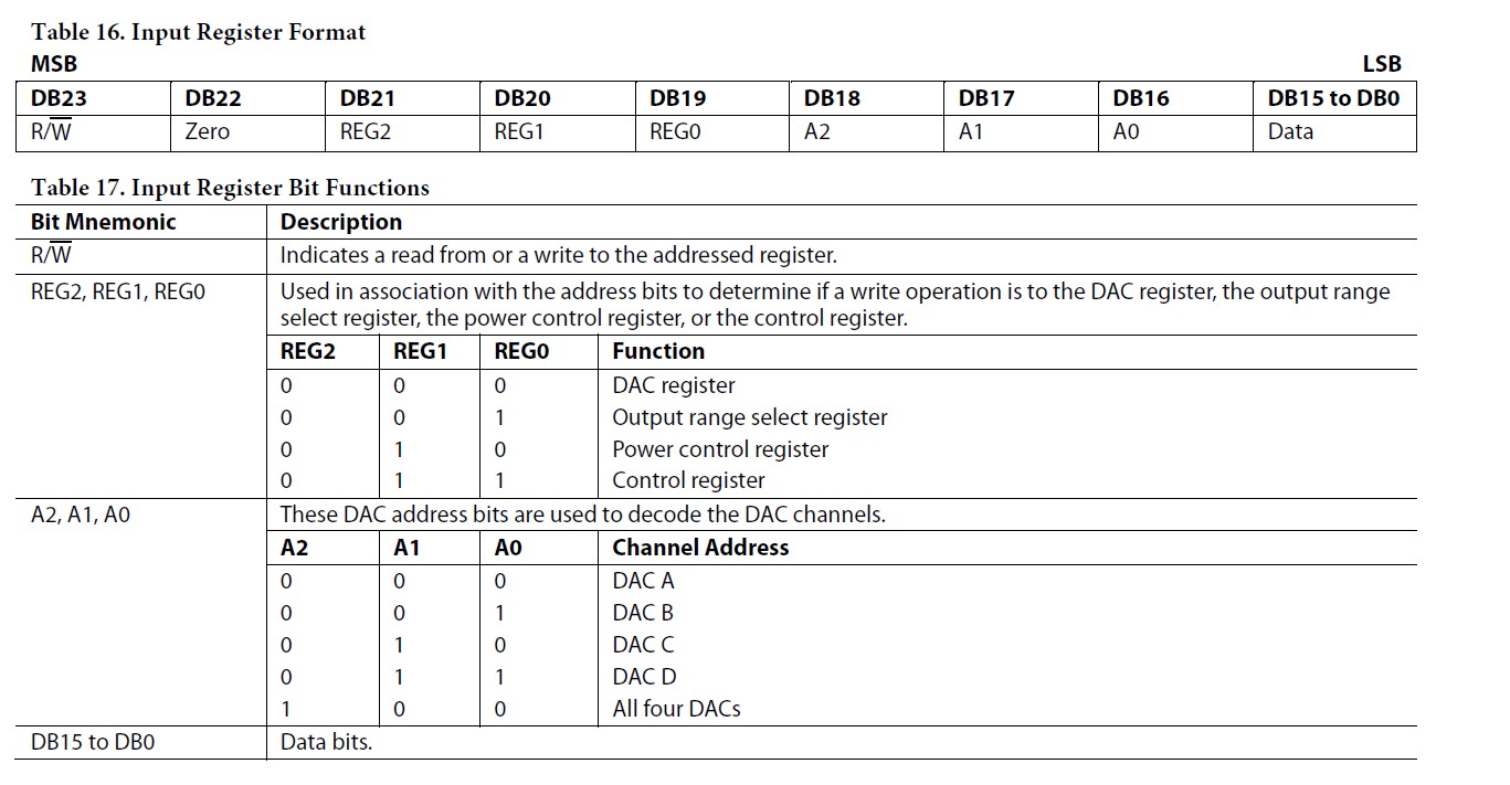
First of all, I need to read carefully the datasheet of the DAC (AD5724) to know how to do the data transmission. The DAC has storage locations (registers) in which the microcontoller can read or write data. Each of these registers has an address that must be specified in the command send from the microcontroller to the DAC. Note: it’s not the same address than in I2C, where every component/chip (for example the pressure sensor I used in week 12) has an hexadecimal address that must be specified to interact with. Here it’s a bit address to talk to a specific register inside the chip.
There is 3 steps that must be done to set an output voltage to the DAC, the order are described in the datasheet and are summerized below.
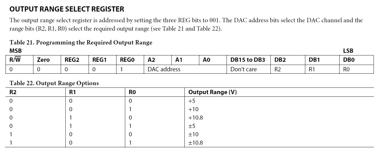
1) Choose voltage range in which we are working because the DAC can have multiple output range
The part of the datasheet below shows how the range selection command must be defined:
- The first bit (MSB) is 0 to tell that we will write something in the register. Note that it’s specified in the datasheet that the MSB is send first for this DAC, but SPI communication can also send LSB first sometimes, in comparison with I2C where MSB is always the first bit.
- Second one is always fixed to 0
- REG2,1,0 are fixed to 001, meaning that we will talk to the “output range select register” by using the address bit 001.
- A2,1,0 specified the DAC address: in the AD5724 DAC, there are 4 independant dac outputs (channels), we thus need to specify for which output we want to select the output voltage range. It can be done output by output or for the 4 outputs.
- The last 3 bits are used to specify the wanted output voltage range (here I want 0-10V range -> 001)
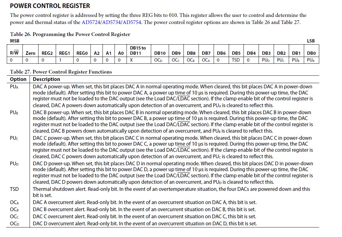
2) Power up the DAC channels that we want to use
We need to write to the power control register to power up the channels/outputs that we will use. One again the command is described in the datasheet.
3) Send the desired output voltage
When the first 2 commands have been sent, the desired output voltage commands can be send to the different output channels. The commands that must be sent are described below, as well as the transfer function given in the datasheet.
The output voltage should be calculated with this transfer function and then encoded on 12 bits (because the DAC has a 12 bits resolution).
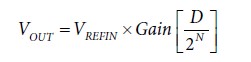
With Vout = the output voltage we want; Vrefin = reference voltage applied at the REFIN pin (for me 2.5V), Gain is an internal gain with a value that depends on the output range selected (speciefied in datasheet, Gain = 4 for my range), N = bit resolution of the DAC, and D the command that will be sent to the DAC.

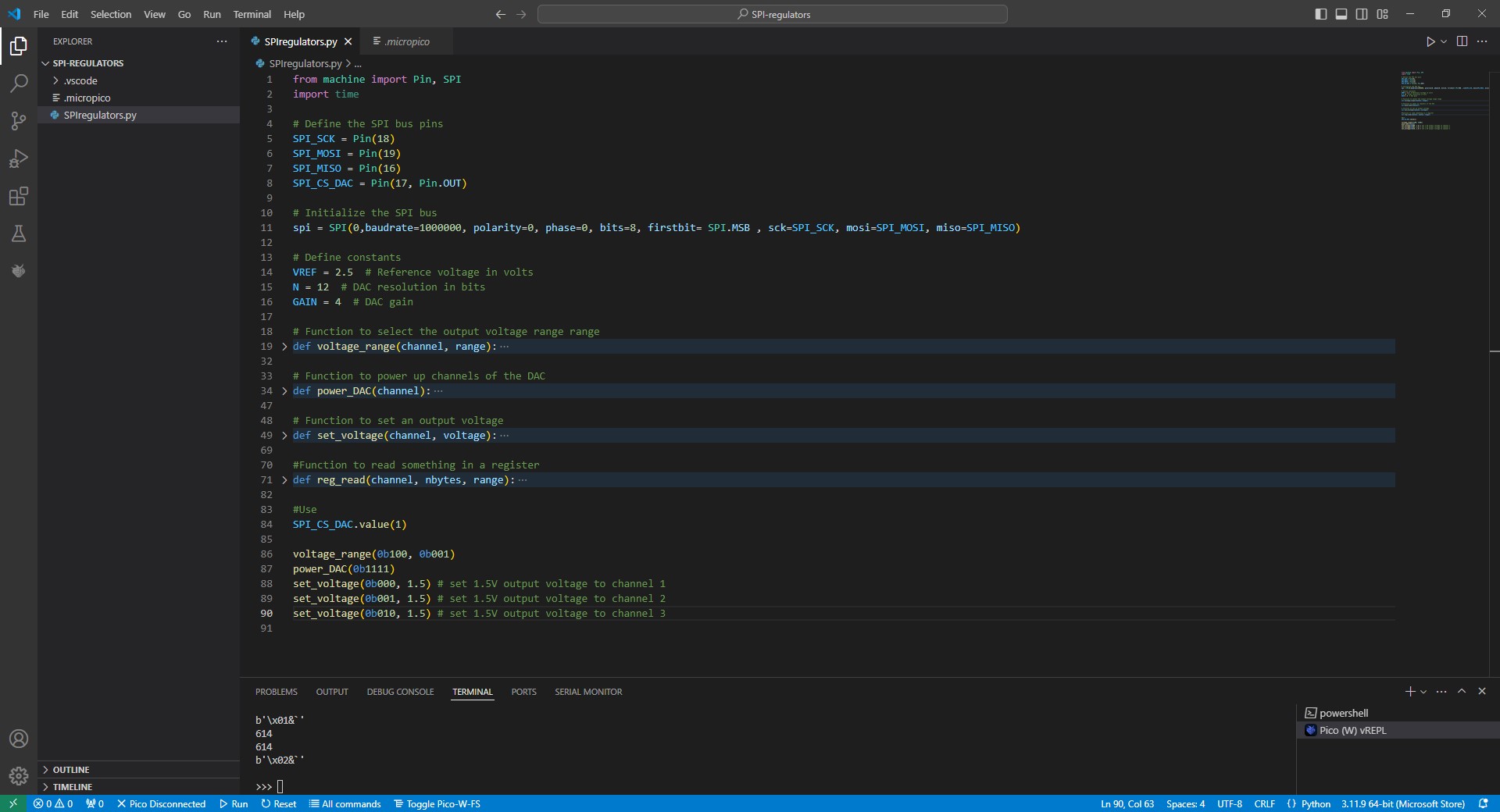
Code
The code follow the same structure as the steps described before.
1) I defined the pin used on my microcontroller (Raspberry pi pico W) and I initiliaze the SPI bus

-
Here I put the usual baudrate that is used for the SPI communication, which is 10MHz. However, my DAC is able to work with a baudrate of 30MHz. That is one of the big advantage of SPI communication: the data exchange can be very fast with this protocole, compared to I2C.
-
Polaity is fixed at zero, meaning that the clock is starting from a low level
- The phase is fixed at 0 as well, meaning that the data exchange will be done on the falling edge of the clock.
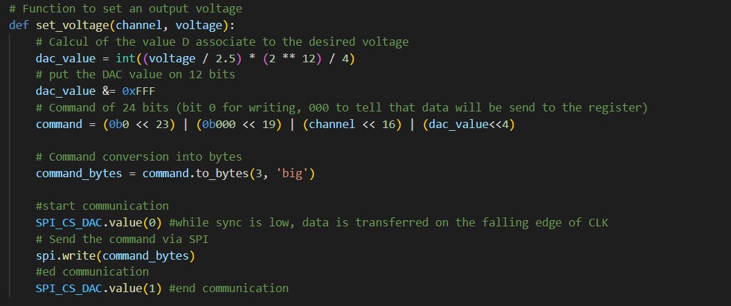
2) I wrote the different function to construct the binary commands that are sent from the microcontroller. The command is constructed based on the details of the datasheet explained above.
Here is the function to construct the command to choose the output voltage range. To start the communication, the CS pin state should be changed from high to low, and put back to the high state when the data exchange is finished.

The others functions are similar but with different command corresponding to the datasheet.

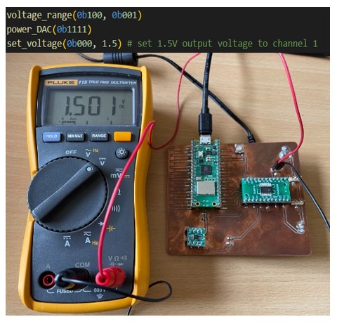
I have tested my ouput voltage by sending the command and used a multimeter to check the output voltage. You can see the result on the picture below:
The whole code can be downloaded here
Note: no need to use already done library!
SPI versus I2C
| Features | I2C | SPI |
|---|---|---|
| Net names | 2 wires: - Serial data (SDA) - Serial clock (SCL) |
4 wires: - Master In, Slave out (MISO) - Master Out, Slave in (MOSI) - Serial clock (SCK) - Chip/Slave select (CS/SS) |
| Signal driving | Open-drain: The line is normally pulled up to a high level by a pull-up resistor, and when any device triggers a signal, the entire line is pulled low. It will avoid | Push-pull: The output pins are capable of actively creating their own logical high and low states (with CMOS), rather than relying on pull up resistors to generate a default state |
| Data rate | Original speed: 100kHz Fast mode: 400 kHz Determined by external pull-up resistor, smaller resistor value means faster transition but higher power consumption. Note that some higher freaquencies can be found in some cases, up to 1MHz. |
Up to 60MHz |
| Adressing | Each component on the bus have an unique address (which is an hexadecimal) that must be specified during the communication. A slave address is sent in 8-bit byte format, MSB first, but the last bit signifies whether the transaction will read or write to the slave. In effect, the upper 7 bits, constitute the slave address, while the 8th bit serves as a READ/WRITE# command bit. On my week week 12, I indeed used the address of the pressure sensor with which I was talking to in my code. |
No address: the state of the CS pin of the chip with which we want to communicate should be changed. |
| Consumption | More consumption link to resistors | Less consumption |
| Way of coding | The data transmitted is always sent eight bits at a time, with an acknowledgement after each byte. For a read operation as in my week 12: The transaction begins with a START bit and is followed by a 7-bit slave address and a direction bit. The slave acknowledges (ACK) the receipt of the address and direction bit and then the slave provides the first byte of data. The master acknowledges the receipt of this byte and then the slave sends the next byte of data. When the master receives the last byte it requires then it responds with a negative acknowledgement to indicate that the slave should not send any more data, and then a STOP bit is sent by the master to complete the transaction and release the I2C bus -> this can be seen on the code I did in week 12. 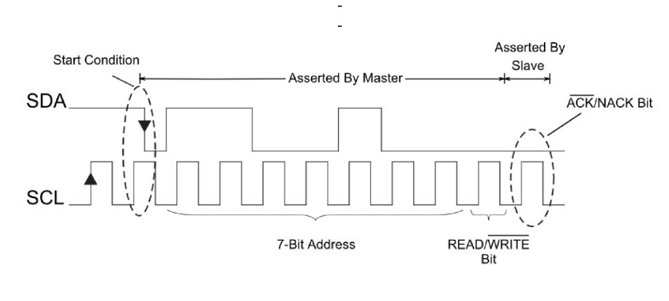 |
The transfer of data does not require acknowledges, it will just be started and ended by the state of the CS pin |
Note these documentation on I2C and SPI from analog devices are very clear if more details are recquired on these protocols.
Note master/slave vocabulary was previsously used and is now replaced by controller/peripherial vocabulary.