8th week Assignment
Electronic Design
Electronic Design
Please for group assignment details visit Anderson Zelarayan Web Page.
We select KiCad to design our boards. To proceed we instaled the Fab library (i/ all FabAcademy listed electronics components) following the instruction at GitLab repository., licensed by Fab Academy and contributors 2021.
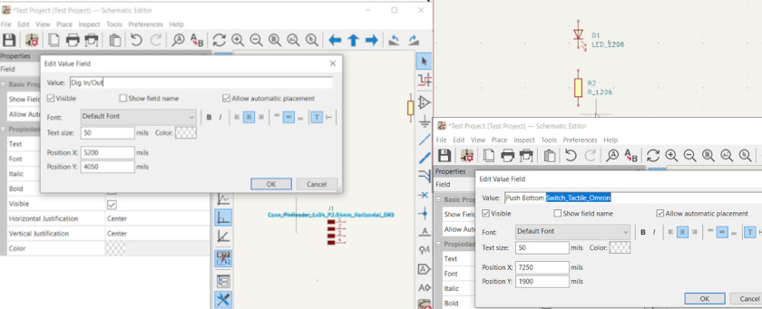
We select Module XIAO RP2040 as a starting point to develop a basic board to interact and communicate with a embedded microcontroller. Thus, it will include a push bottom and a LED. Based on this minimun components we proceed to work on our project schematic. The electronic components considered as listed as follow:
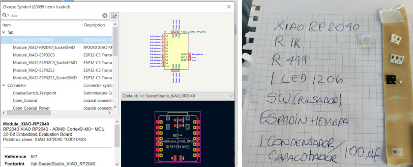
When working on schematics, we need to be careful with labeling each component in/out or GND
adequately. This means that each component pins label must be the same with the ones labaled at the
board. This to avoid problems when working on PCB Editor
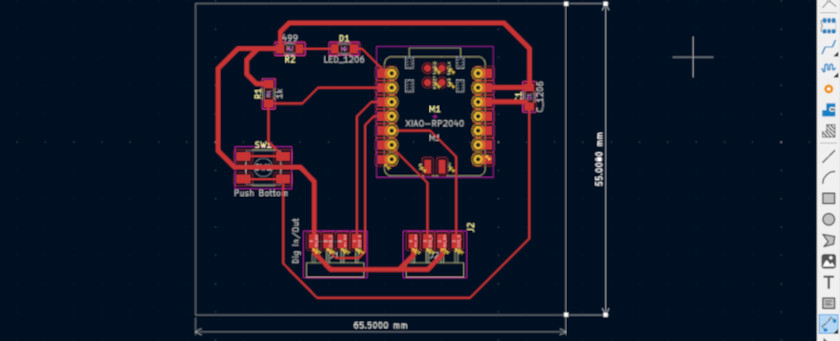
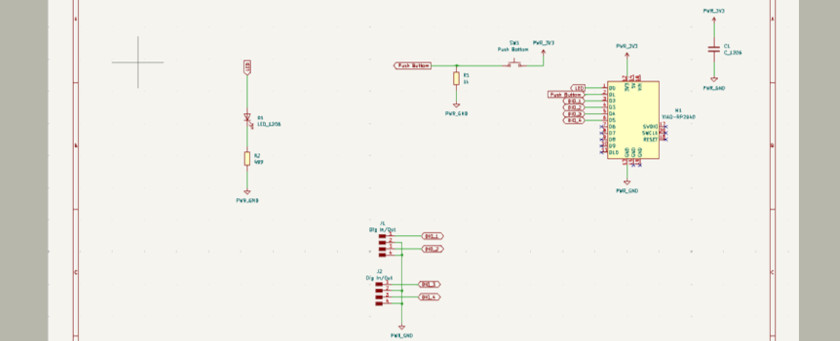
This is the schematic where you can see all the components. You can download Schematic design file and
the PNG file here.
PCB Designing
To obtain PCB design and fabricate it, we need to take the following steps:
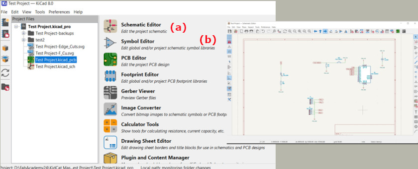
Select the PCB Editor File from the KiCad Principal Menu.
Update PCB from Schemnatic option located at Tools Menu on PCB Editor.
Set track sizes (width) and appereance (material) option located at Edit Board
SetUp Menu. Here we set 0.4 for traces width and 0.8 for ground traces.
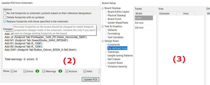
Setup constraints option located at Edit Board SetUp Menu. The most important it is
to setup cleareance at 0.4 to no exceed the end mill diameter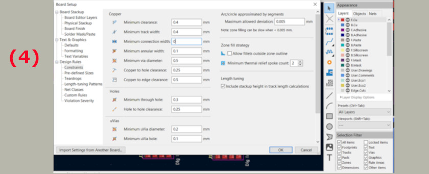
Start drawing the traces selecting width and layer correctly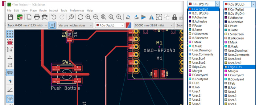
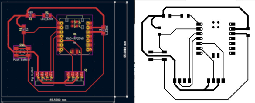
This is the pcb design where you can see all the components. You can download design file and
the SVG files here.
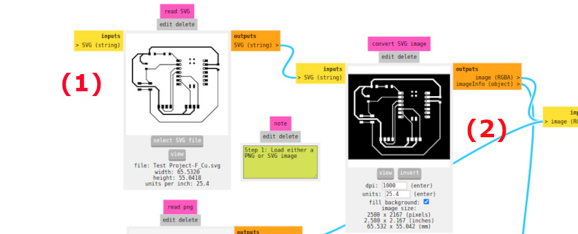
To fabricate PCB design we use SVG files applying following steps within FabModules Software:
Upload SVG Board file.
Convert SVG image inverted it using 1000dpi.
Set mill traces (material) using 1/64" end mill (select 2 as offsetting number).
Calculated Mill raster 2D.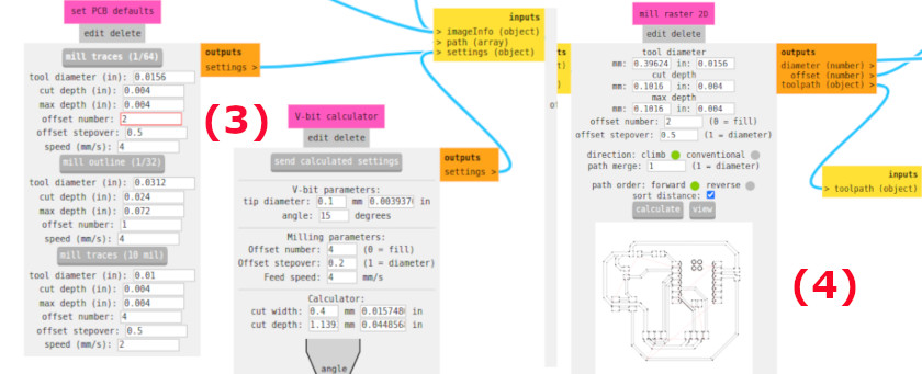
Visualize the image selecting width and material correctlyApplied same steps for Cutting Edges but use 1/32" End Mill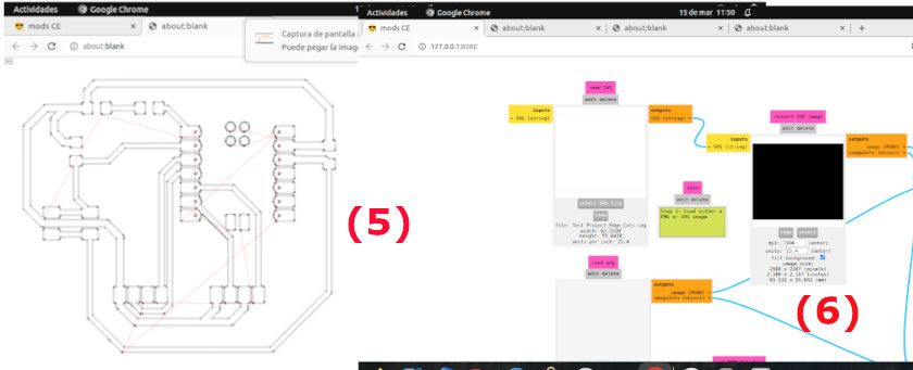
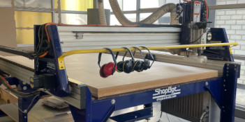
The machining was made with a Modela MDX-20 in two parts. First traces using 1/64¨ y secondly cutting the edges using 1/32¨ end mills.
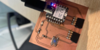
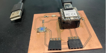
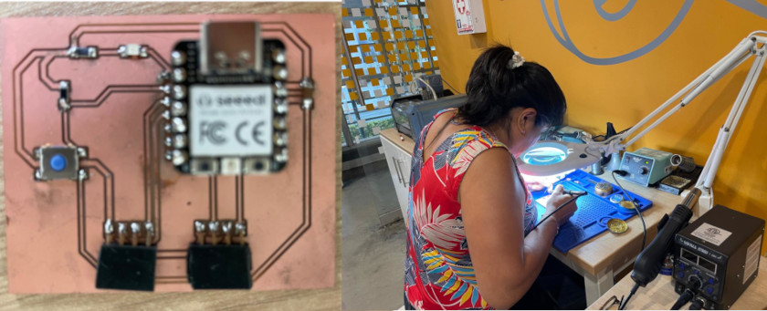
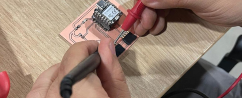
To proceed with soldering I fix the PCB with double contact tape. Thus, we can avoid any movement when tin soldering
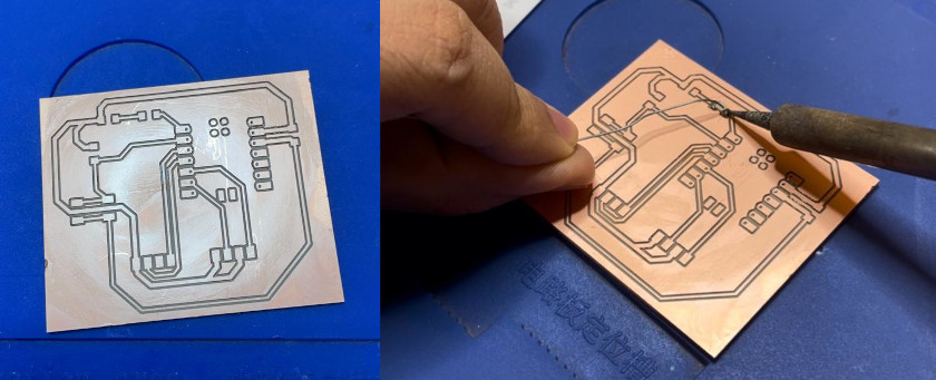
The following photo shows the final result and the soldering process
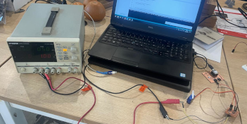
The testing process was undertake in two steps:
Open Arduino IDE software.Connect the serial port to the board (RP2040).File.Examples. 01.Basics-Blink. which turns an LED on
for one second, then off for one second, repeatedly.
// the setup function runs once when you press reset or power the board
void setup() {
  // initialize digital pin LED_BUILTIN as an output.
  pinMode(26, OUTPUT);
}

// the loop function runs over and over again forever
void loop() {
  digitalWrite(26, HIGH);  // turn the LED on (HIGH is the voltage level)
  delay(1000);                      // wait for a second
  digitalWrite(26, LOW);   // turn the LED off by making the voltage LOW
  delay(1000);                      // wait for a second
}
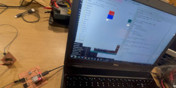
upload the codeinto the XIAO RP2040 like shown in the folowing videorun the program and check for LED lightining like shown in the video below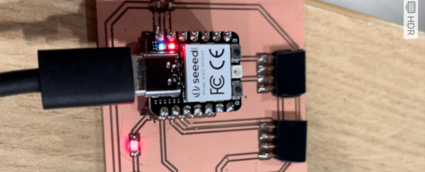
You can get access to the LED code here.

Wellcome to the process of trying to make almost something