WEEK 8
Electronics design
Group Assignment:
- Use the test equipment in your lab to observe the operation of a microcontroller circuit board
- Send a PCB out to a board house
Individual Assignment:
- use an EDA tool to design a development board to interact and communicate with an embedded microcontroller, produce it, and test it
- Extra credit: Try another design workflow
- extra credit: Design a case for it
- extra credit: Simulate its operation
This week, I learned to design electronic boards using KiCad software, to measure some microcontroller signals using an oscilloscope and a multimeter. I also revisited using the milling machine to make electronic boards, used the Arduino IDE for microcontroller programming, and got back into 3D designing and printing. It was a week where I used various manufacturing technologies to complete the assignments, which I really enjoyed.
Group Assignment
In the group assignment, we made some measurements of the microcontroller signals. We were interested in measuring the PWM signals, so we used a potentiometer connected to a Quentorres board that we made during the electronic production week.
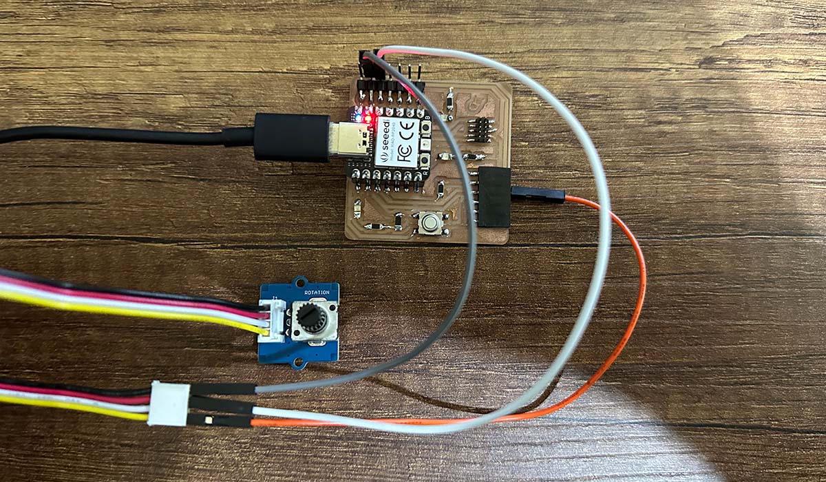
We also used this small program that changes the intensity of an LED when a potentiometer is turned. The LED is connected to pin 26, and the potentiometer's signal enters through pin 28.
void setup() {
// put your setup code here, to run once:
    Serial.begin(9600);
    pinMode(28, INPUT);
    pinMode(26,OUTPUT);
}
void loop()
{
    int sensor_value = analogRead(28);
    Serial.println(sensor_value);
    int led_value;
    led_value=map(sensor_value, 0, 1023, 0, 255);
    analogWrite(26,led_value);
    delay(50);
}
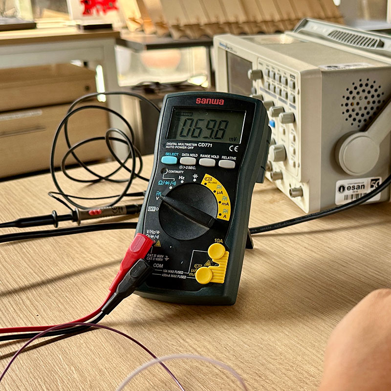
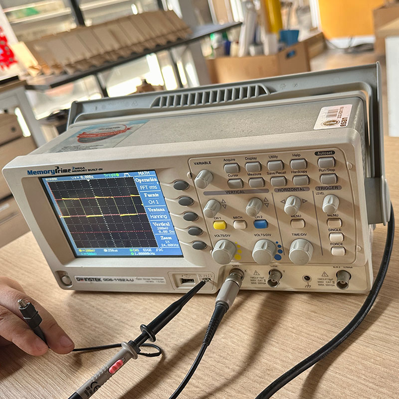
The measuring instruments we used were a multimeter and an oscilloscope.
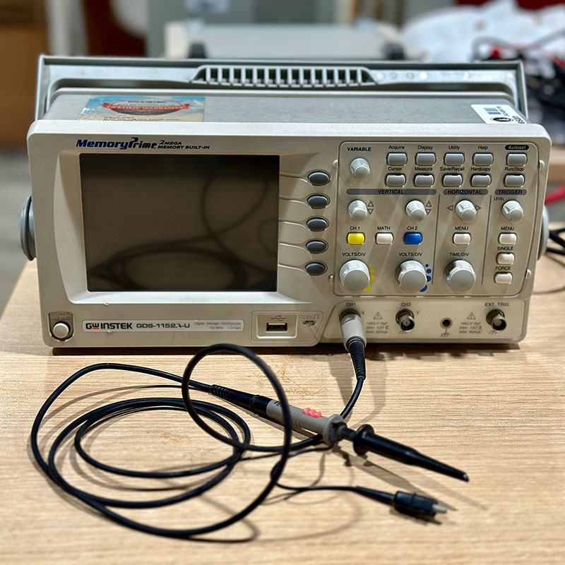
The first thing we did was calibrate the oscilloscope. To do this, we connected the main probe to the calibration terminal and then pressed the AUTOSET button. As can be seen in the following images, once the calibration is correct, a square wave signal is observed.
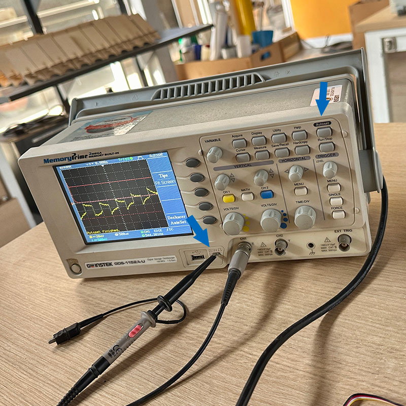
In the next test, we measured the signal coming out of pin 26, which controls the LED's intensity while we rotate the potentiometer. You can see how the time the signal stays high changes from 0% to 100%.
Then, we can see how this PWM signal is interpreted as voltage. By measuring the same signal from pin 26 with the voltmeter, we can see how the value changes from 0 to 3.3 volts.
Individual Assignment
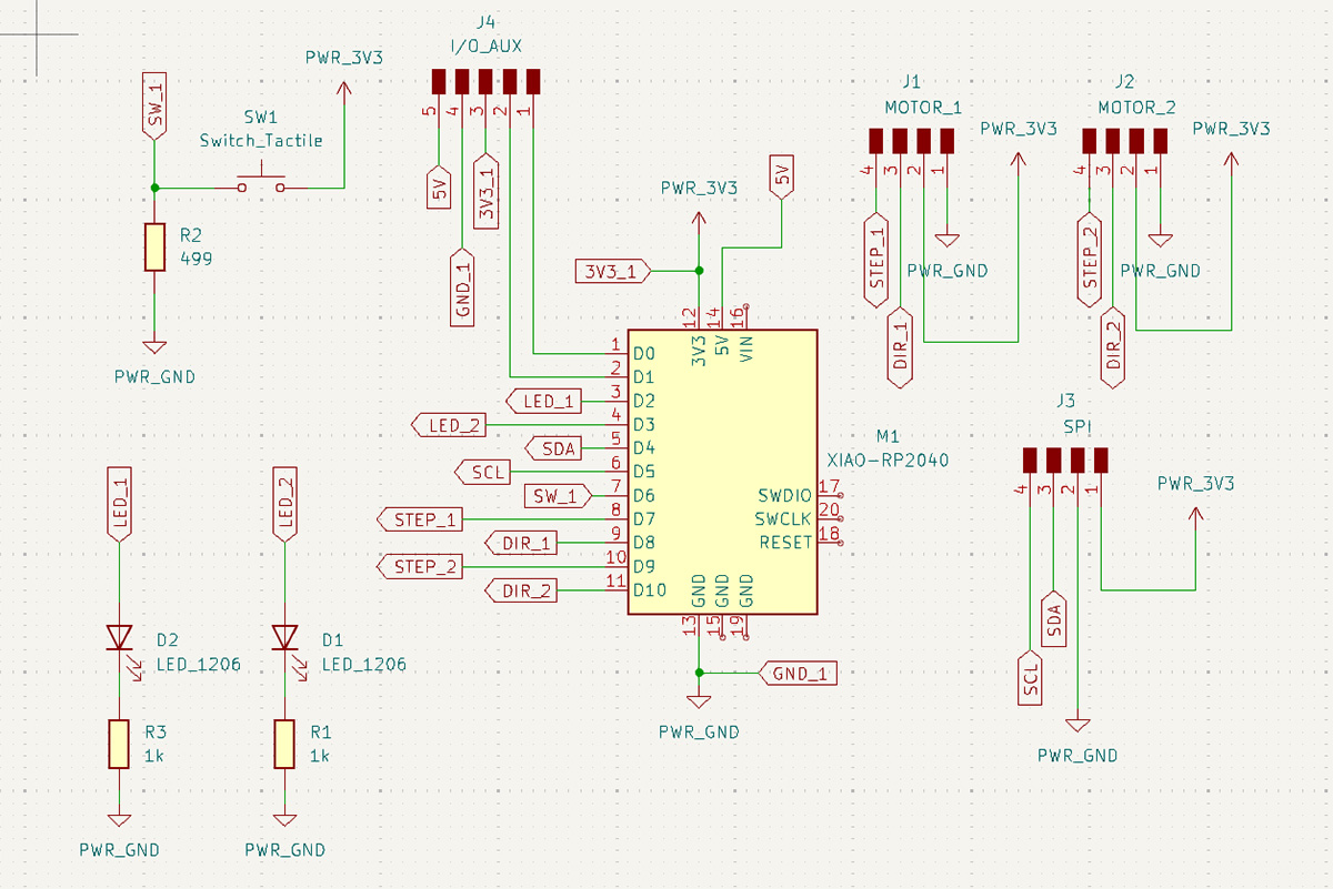
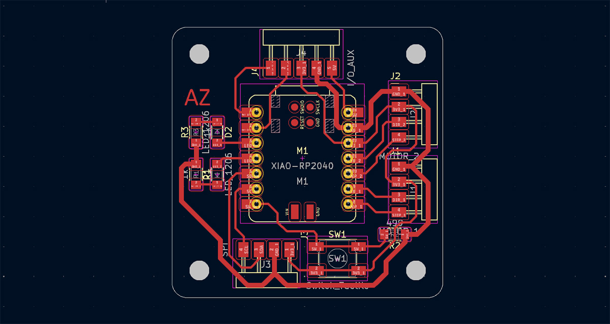
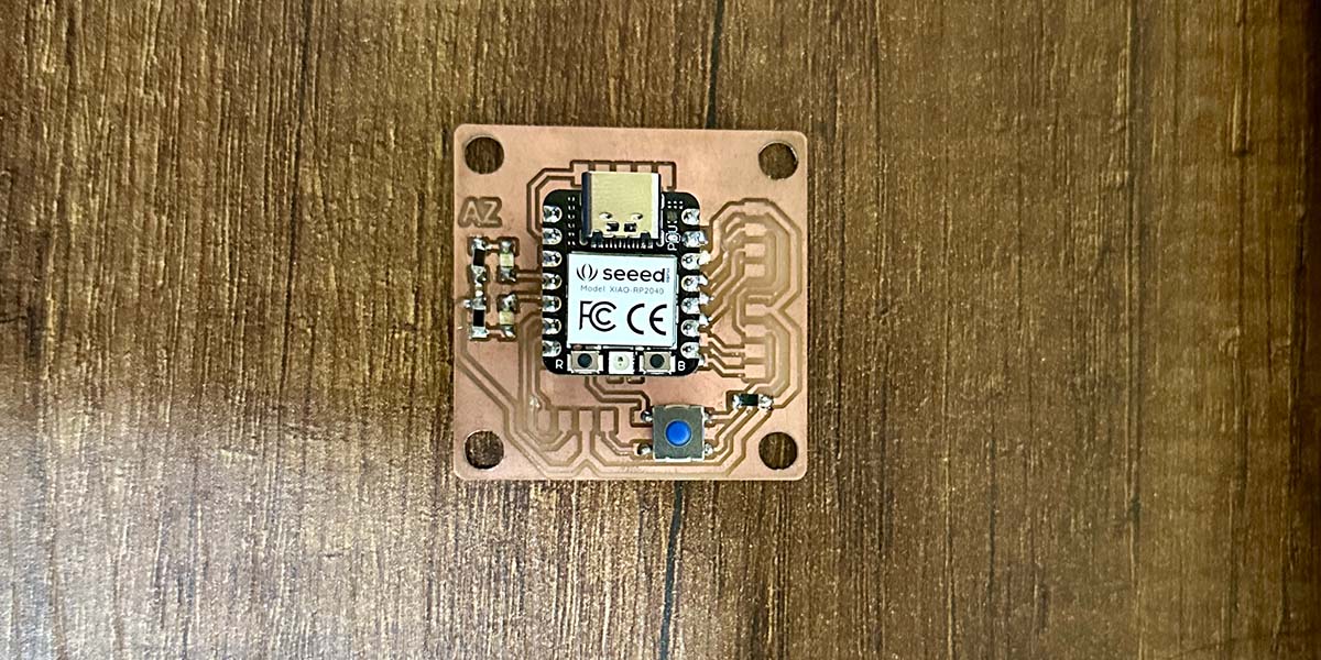
For the individual part, I designed a board similar to the Quentorres board, which essentially has several connectors allowing it to connect to other boards, such as stepper motors board and sensors boards. I also included two indicator LEDs and a push button.
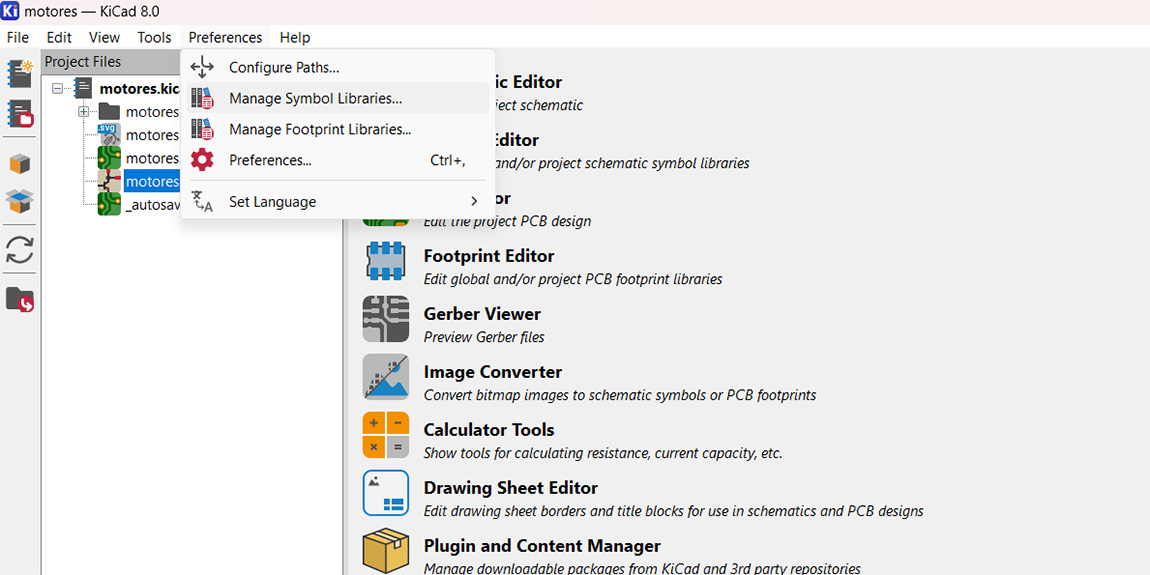
To carry out the design, I used KiCad EDA, which is quite intuitive and easy to use. This software allows for the creation of schematics, PCBs, and also 3D models of the boards.

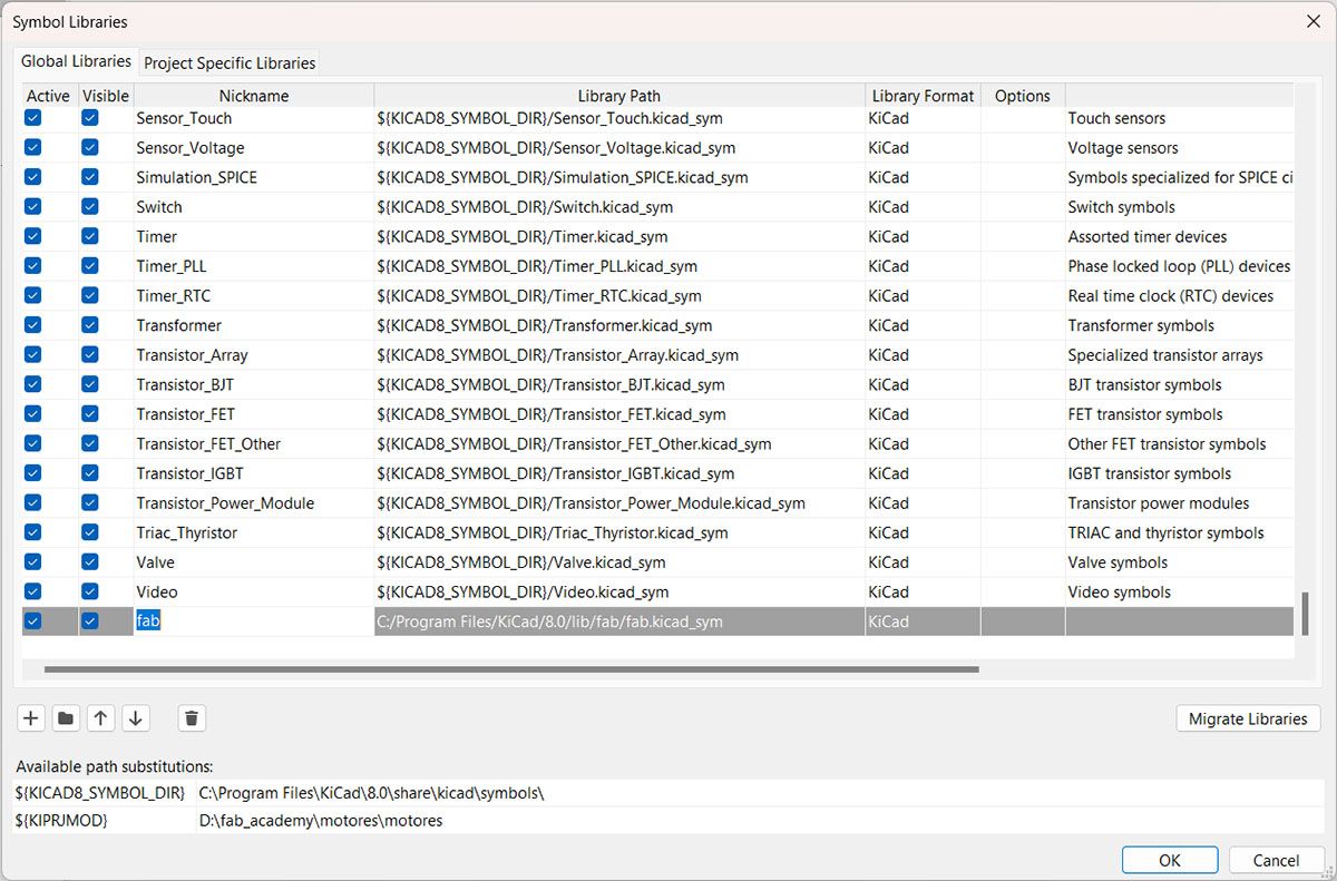
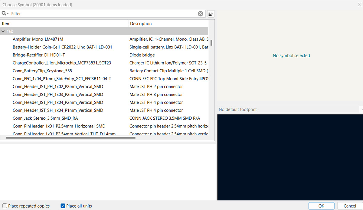
The first thing I did was add the Fab electronics component library.
First, I added the symbol library.
Second, I added the footprint library
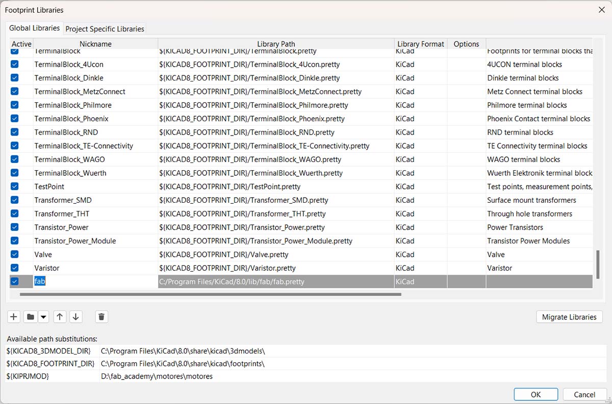
Once the libraries have been added, you can select the components from the schematic window.
After finishing the necessary configurations, I started doing the circuit with the components shown in the following image. This board is able to control two stepper motors, which is why the board has two connectors, J1 and J2, connected to pins that support PWM. This board can also be connected to a sensor that uses the SPI protocol, for which there is the J3 connector. The board also has two LED indicators and a push button.
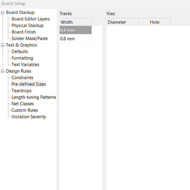
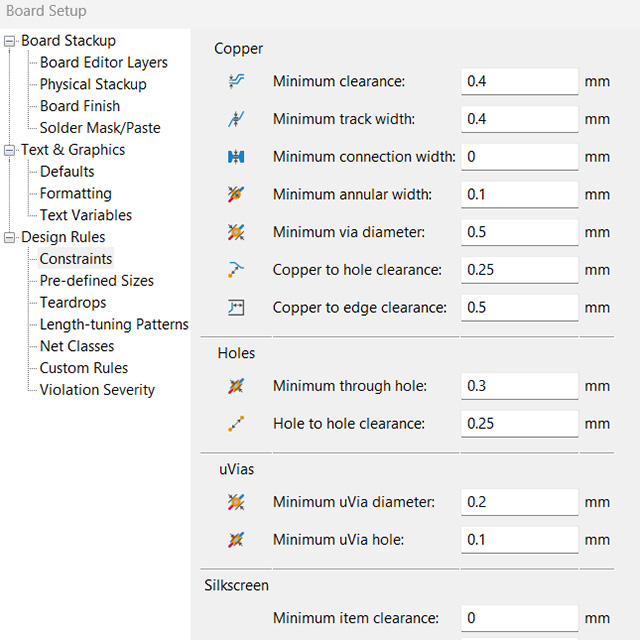
After finishing the schematic, the next step is to make the PCB. Before that, I created two predefined track widths of 0.4 mm and 0.8 mm. I used the 0.8 mm width for the ground connections. From 'constraints', I also defined the minimum clearance at 0.4 mm, which corresponds to the smallest mill I will use, and the minimum track width at 0.4 mm.
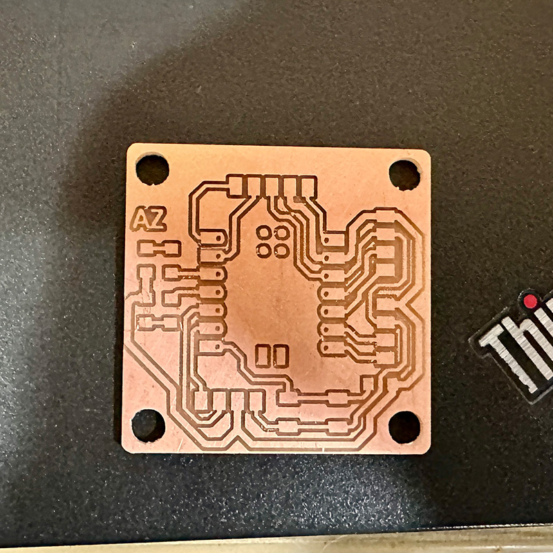
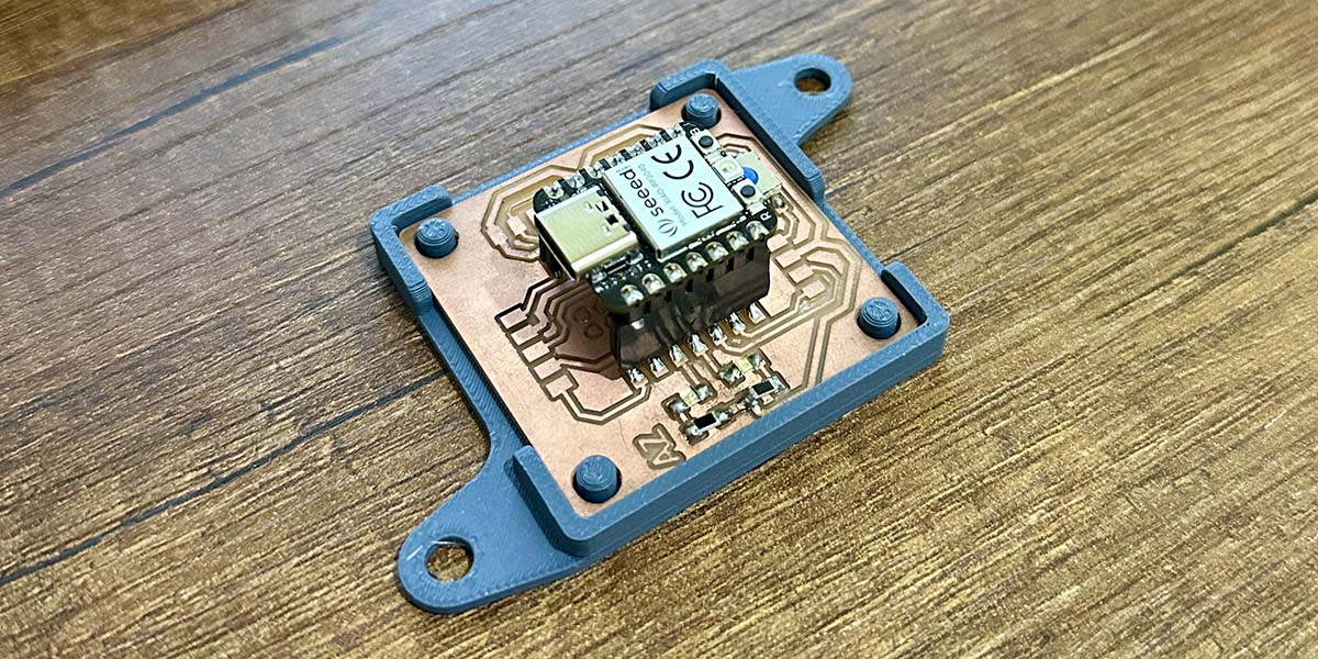
This is the result of the board I designed; I also added four holes that will allow it to be fixed to a case for protection. I tried to place the components as close as possible to have a small board. As a result, the board measures 45 x 45 mm. The holes are spaced 36 mm apart.
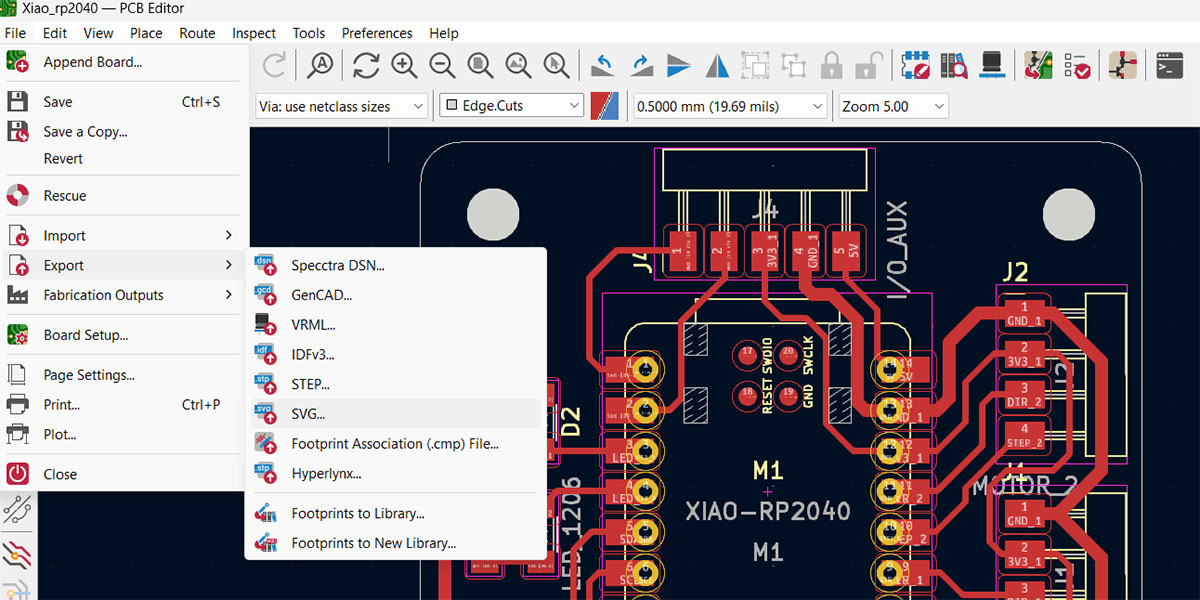
After finishing the PCB, we need to export it in a format that can be read by the mods, which could be a PNG or SVG image. In this case, KiCad allows exporting it in SVG format.
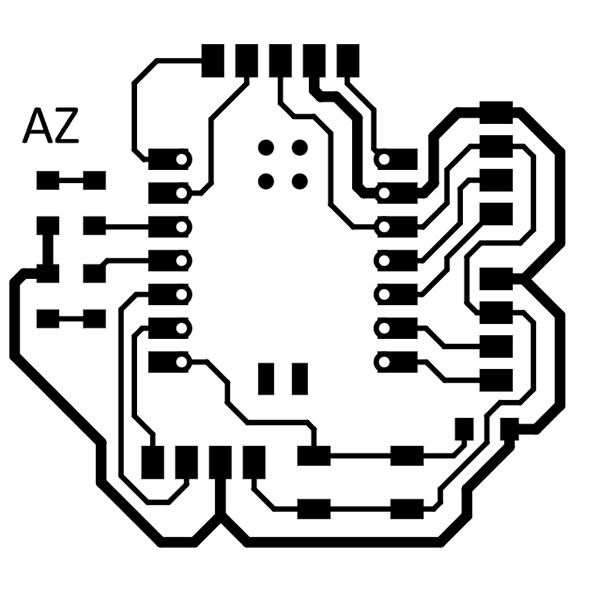
These are the images of traces, as well as the mounting holes. KiCad allows drawing on different layers, so you can export each file separately. This is important because some of the milling needs to be done with a different tool.

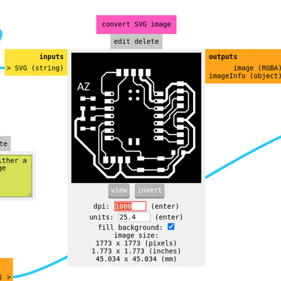
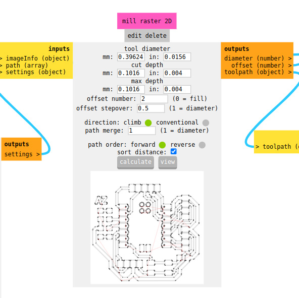
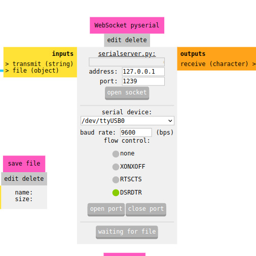
Now it's time to mill the boards I designed. For this task, I used the Modela MDX-20 milling machine and the Mods CE application. As shown in the following images, I first imported the image in SVG format; it was necessary to invert the image and set it to 1000 dpi. I used a 1/32” mill for the cuts and a 1/64” mill for the traces.
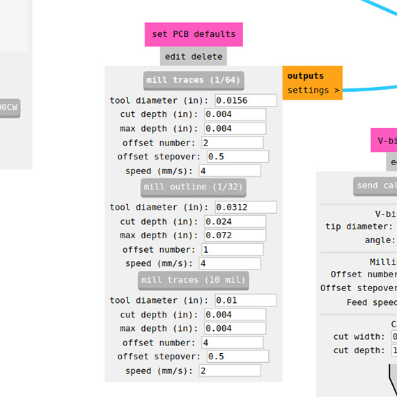
Once the tool is selected, we proceed to calculate the toolpaths and send the file. It's also important to mention that initially, the Z-axis should be recalibrated when changing tools
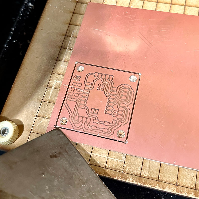
This is the result of the board after milling.
Then, follows the soldering and testing stages. For the tests, use the following program, which I also showed during the embedded programming week. It consists of turning on the LEDs each time the button is pressed.
void setup() {
// put your setup code here, to run once:
pinMode (26, OUTPUT);
pinMode (0, OUTPUT);
pinMode (1, OUTPUT);
pinMode (27, INPUT);
}
void loop() {
// put your main code here, to run repeatedly:
int state=digitalRead(27);
if (state==HIGH){
digitalWrite(26,HIGH);
digitalWrite(0,HIGH);
digitalWrite(1,HIGH);
}
else {
digitalWrite(26,LOW);
digitalWrite(0,LOW);
digitalWrite(1,LOW);
}
}
Next, the results of the tests.
Finally designed a small case that will protect the board and allow it to be mounted on a surface. It has mounting holes as well as space in the walls for the connections.
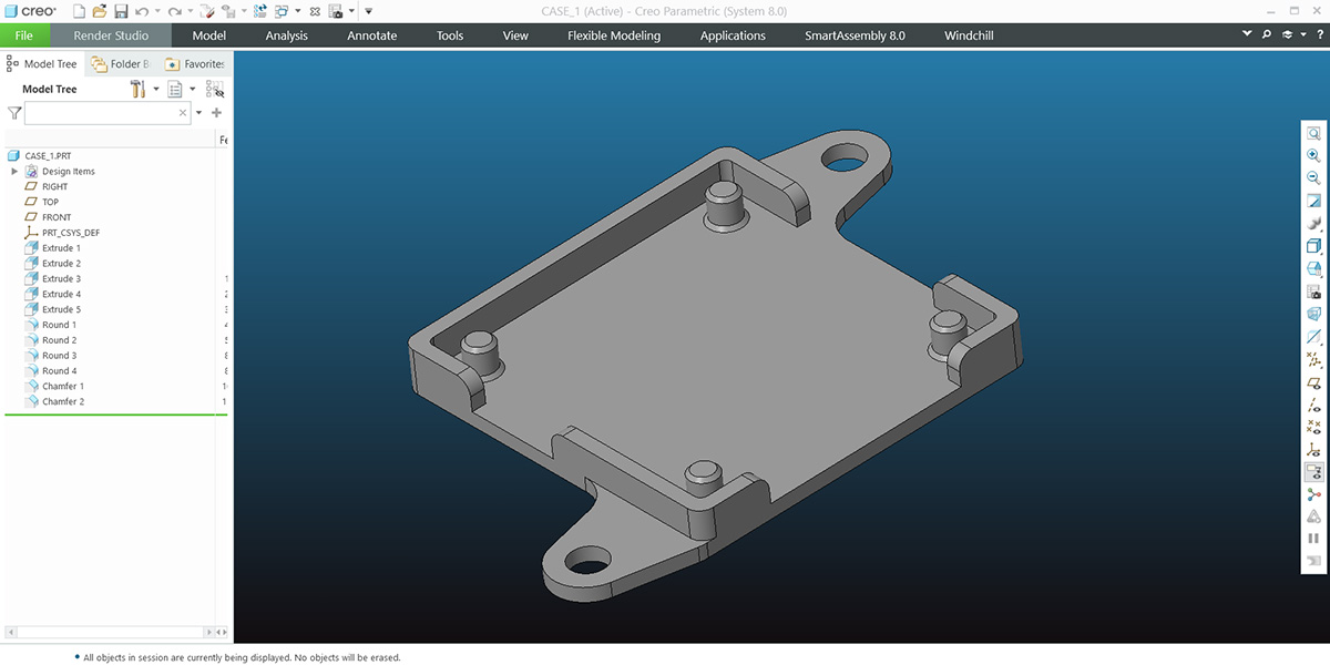
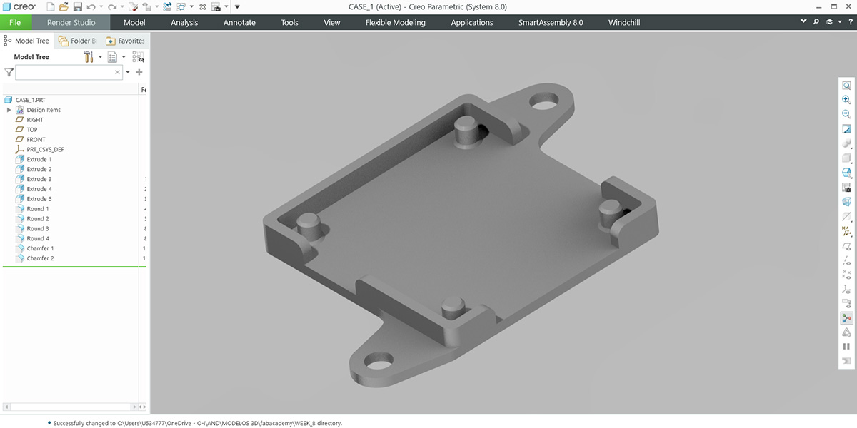
This is how they look with the case.
Download:
Here you can download de files of milling in SVG format: