PCB Production
Milling
I sent the GBR job of my PCB to the milling machine and ran it.
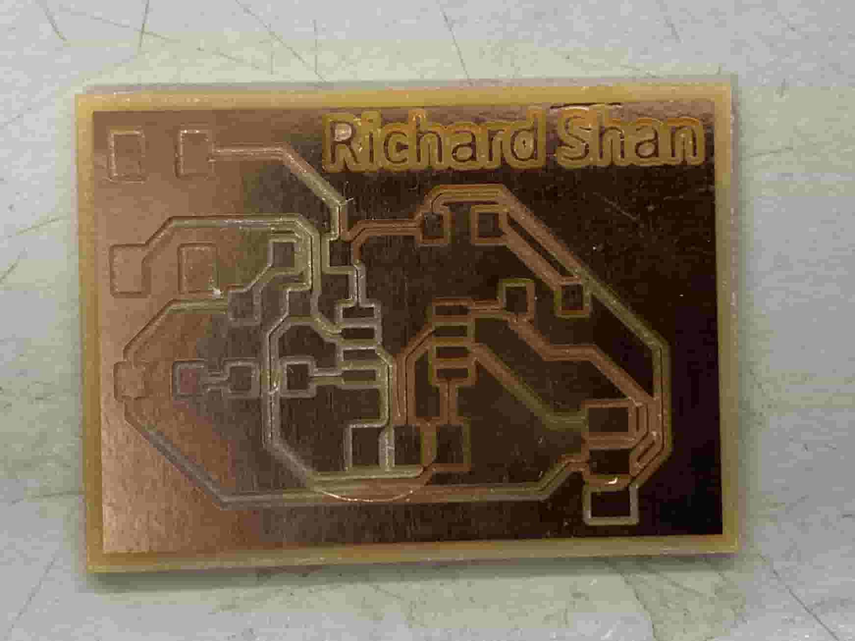
However, after I ran the job, I saw that the traces were incredibly thin and the clearance was as well. To fix this, I went back into KiCAD's PCB Editor and changed the trace size from 0.2mm to 0.5mm. Additionally, I changed the trace clearance in Bantam Tools from 0.15mm to 1.5mm.
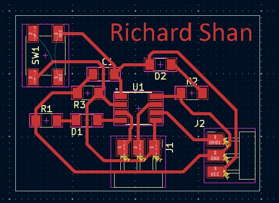
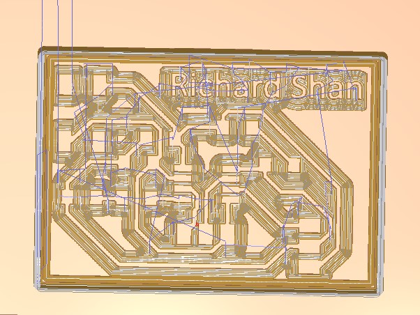
The render in Bantam looked good.
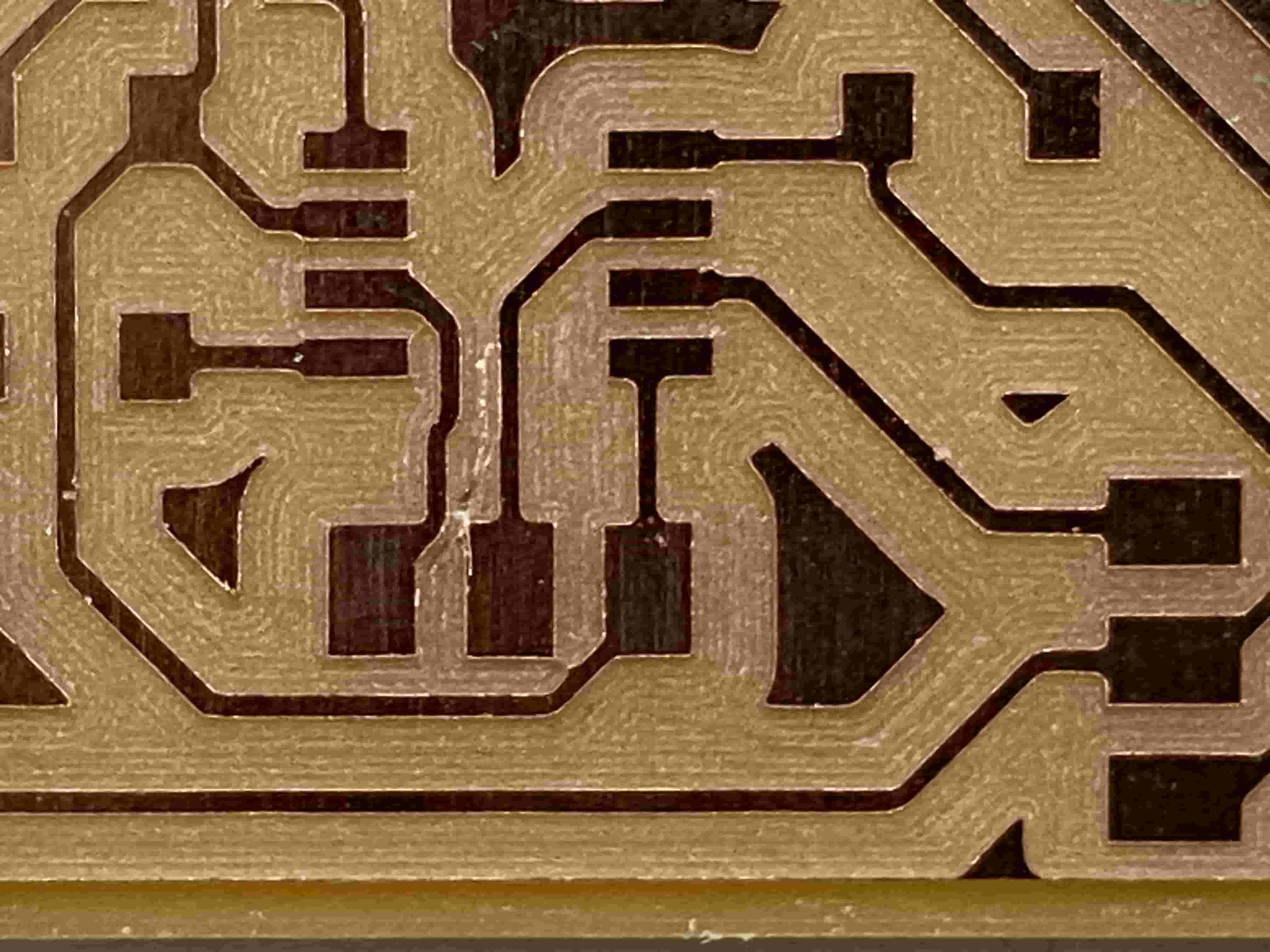
I then cut the board. Although this job took longer, the traces look a lot better. However, I happened to choose a bad bit and as such, the edge cutout was a little rough but everything overall looks good.
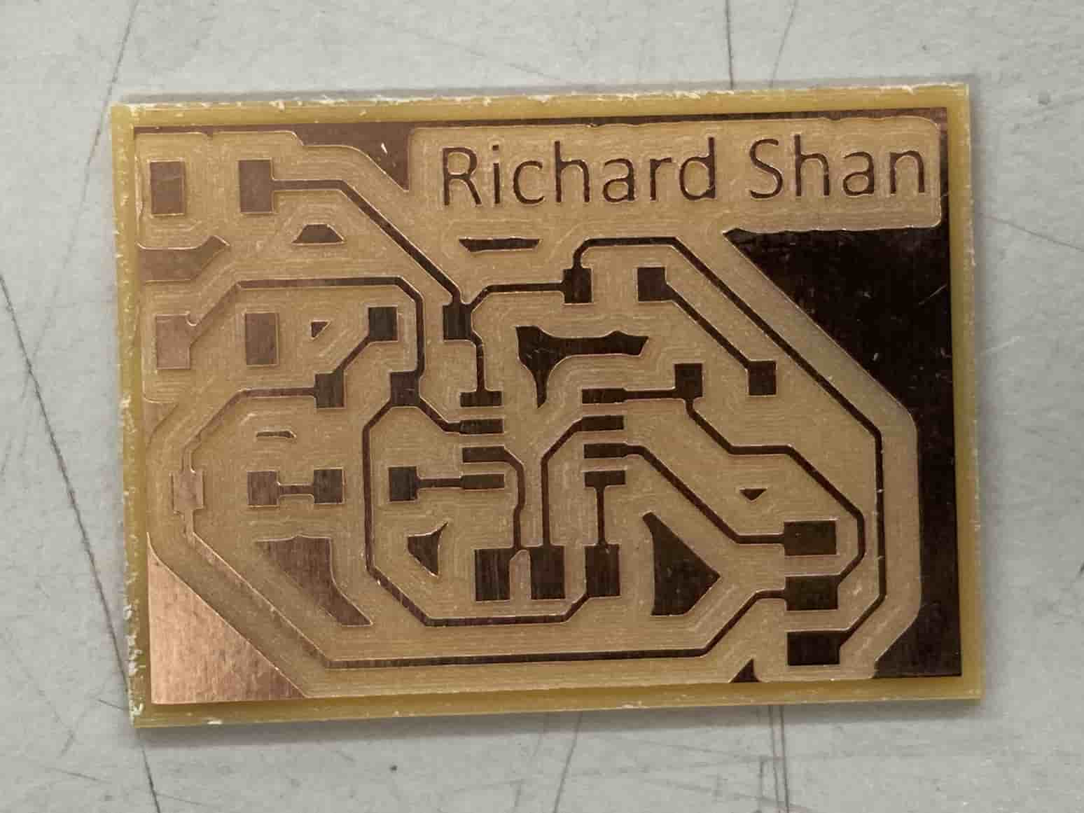
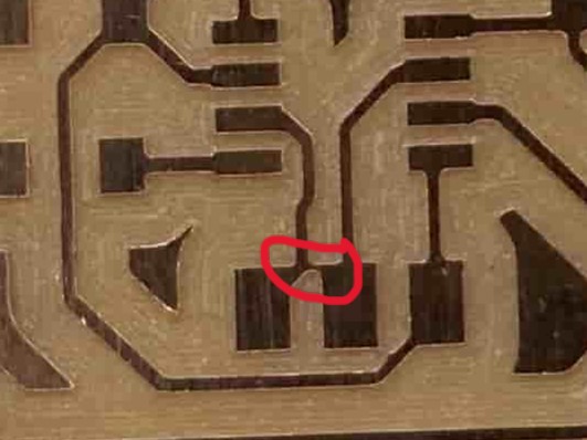
One of my connector headers had a bridge between two trace pads that I had to manually fix with a razor blade. After I manually separated the traces, the board is ready for soldering.
 |
 |