Custom PCB Design
For this week, I was assigned the task to use an EDA tool to design a development board to interact and communicate with an embedded microcontroller, produce it, and test it.
KiCAD
To actually design the board, I had two main choices: Eagle or KiCAD. I ended up choosing KiCAD after doing some research online because it seemed that KiCAD was more popular among experts. Additionally, KiCAD is completely free and would allow me to continue designing PCBs, unlike Eagle which required a ongoing license.
Setup
I first downloaded the installer for KiCAD here. I then ran the installer to actually download KiCAD.

Before I started designing, I downloaded the KiCAD Fab Library. This download came with both symbol libraries, used in the designing of the schematic, and footprint libraries, used for designing the actual board.
I first added the symbol library (fab.kicad_sym) by opening Preferences -> Manage Symbol Libraries inside the schematic editor. Here, I can see all of my installed libraries, which currently are just the defaults.
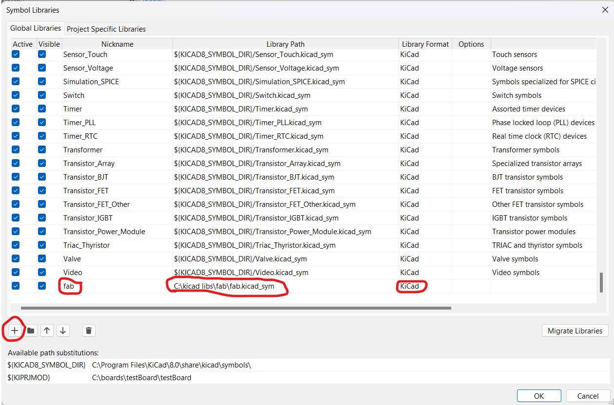
I then clicked the Plus icon in the bottom left of the interface, allowing me to enter in the details for referencing a new library. I named the library "fab" and pasted in the absolute file directory path to the fab library file. I selected "KiCAD" as the library format as the library is a .kicad_sym file. Other third party or older libraries end in the .lib extension, and importing one of those would use the "Legacy" library format option.
I then repeated this process for the footprint library. To open the footprint libraries editor, I first opened the Assign Footprints menu from the Schematic editor via Tools -> Assign Footprints. Inside of the Assign Footprints menu, I opened the Footprints Libraries editor through Preferences -> Manage Footprint Libraries. This menu is similar to the symbol libraries manager in that it allows me to view and edit all installed footprint libraries. I used the Plus icon to create a new row in the table, and pasted in the absolute path to the Fab footprint library from the downloaded fab library.
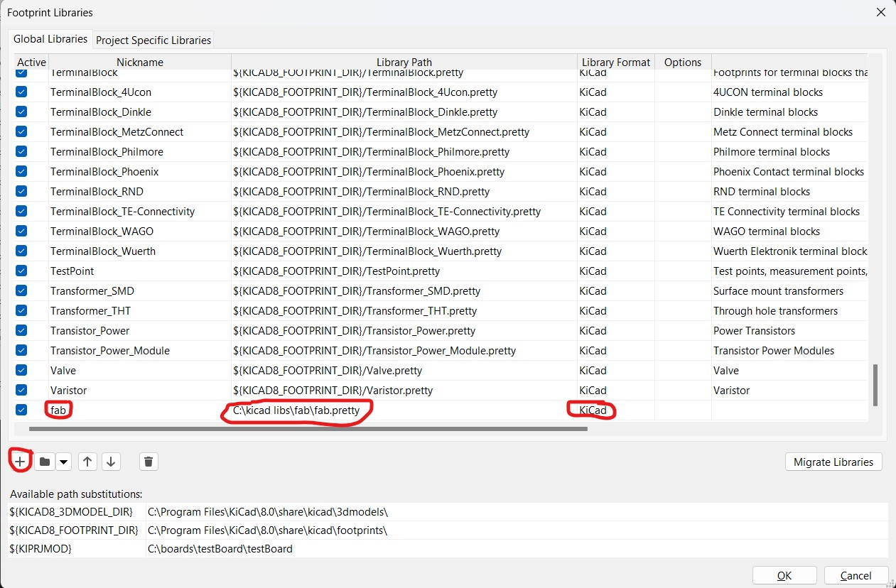
I named the footprint library "fab". I am able to use the same footprint library name as my symbol library without running into a duplicate variable name error as the two types of libraries are handled by separate and respective library managers. I then inputted the path to the fab.pretty folder inside my Fab library download. This folder contains a bunch of components and their individual *.kicad_mod files. I chose "KiCAD" as the library format because I was using a *.pretty folder which contained all the information for the footprints I was importing.
After importing the libraries, I was ready to start designing.
Practice Board
Before I designed the board that I would actually use, I went through the entire design process with a simple ATTiny412 LED board.
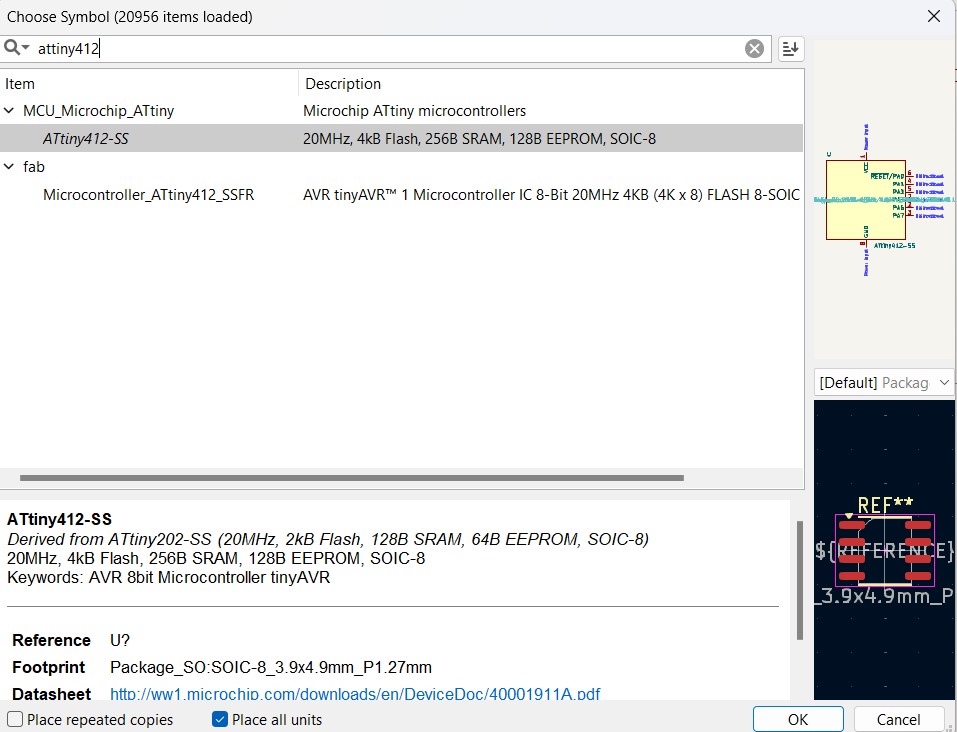
To add a component in the schematic editor, I used the keyboard shortcut of a and searching for the name of the symbol. In this image, I am adding the symbol for the ATTiny412 chip by opening the Choose Symbol UI and searching for the ATTiny.
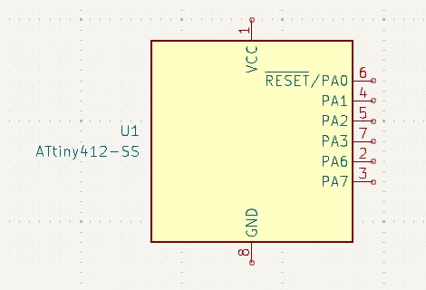
I then clicked OK and clicked to place down the ATTiny symbol. Here is the ATTiny now in the schematic.
I then repeated this process for each of my components. I added a capacitor, pin header connectors, a resistor, and an LED.
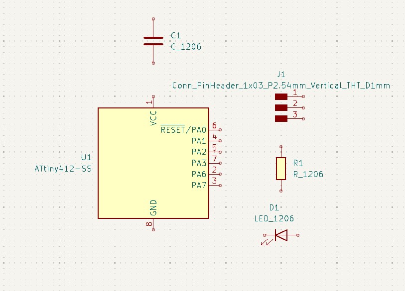
I then used the w keyboard shortcut to access the wiring tool. I placed wires to connect each respective part of the circuit. Because I didn't want my schematic to be too messy, I used the label function (CTRL + L) to help organize my circuit. For example, the LED label on pin 4 and the LED label adjacent to the resistor is recognized by KiCAD as a wiring connection between pin 4 and the resistor.
I then opened the PCB editor for this schematic and started routing the traces via the X keyboard shortcut for the Route tracks function. This function allows me to use my mouse to route traces between two connected components. Here is what my board looks like after routing all my tracks.
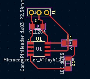
Next, I added an outline edge cut by using the line and arc functions. This allows me to create a outline for the board that will actually cut it out of the copper.
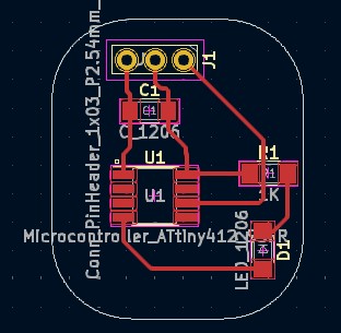
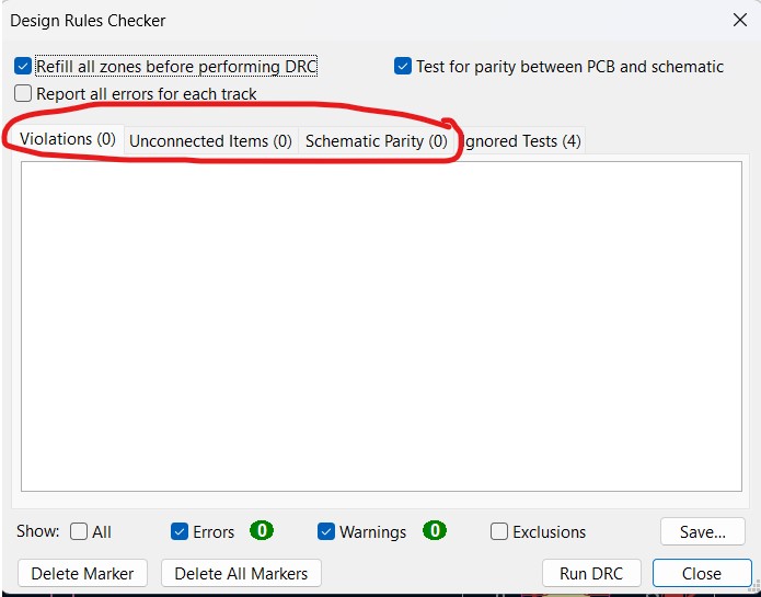
After adding edges, my board's design is complete. I checked that there were no errors using the Design Rules Checker or DRC, found inside the PCB editor under Inspect -> Design Rules Checker. After running it, I had no errors. (Side note: I'm not exactly sure what the "Ignore Tests" are. I assume that these tests are disabled by default and thus probably not a big deal.)
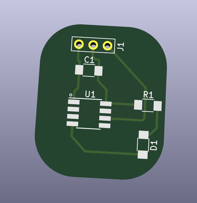
I then rendered the PCB in 3D by using the 3D Viewer, accessed by using the Alt + 3 shortcut inside the PCB editor or through View -> 3D Viewer. Here is a picture of my rendered board.
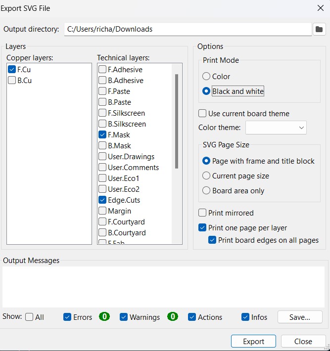
Next, I exported my design as a series of SVG files via File -> Export -> SVG. I exported the F.Cu copper layer and the F.Mask and Edge.Cuts technical layers in black and white coloration. Here are my settings for the export.
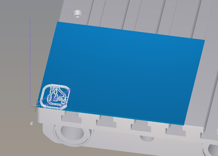
I then used the programs -> open program -> machines -> Othermill-Bantam Tools -> PCB function in Mods to turn my SVGs into millable .nc files. I then imported them into Bantam Tools to make sure that everything looked good.
Board Design
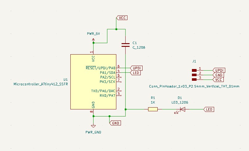
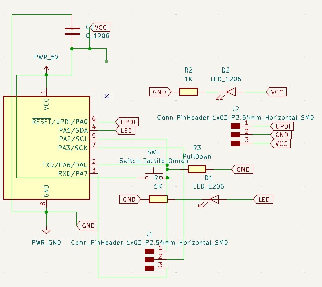
For the board that I would actually mill, I included a capacitor for the power ground, an LED power indicator, a programmable LED, a button, and some blank connector headers. Since this board design is similar to the practice board I made, I copied that design and made a few edits. Here is the schematic of the board.
I then opened up the board in the PCB editor and created the routes. This was by far the longest process as I spent around an hour working through 3-4 different iterations of the board to create a working and decently compact routing. Thank you Collin Kanofsky for helping me with the traces.
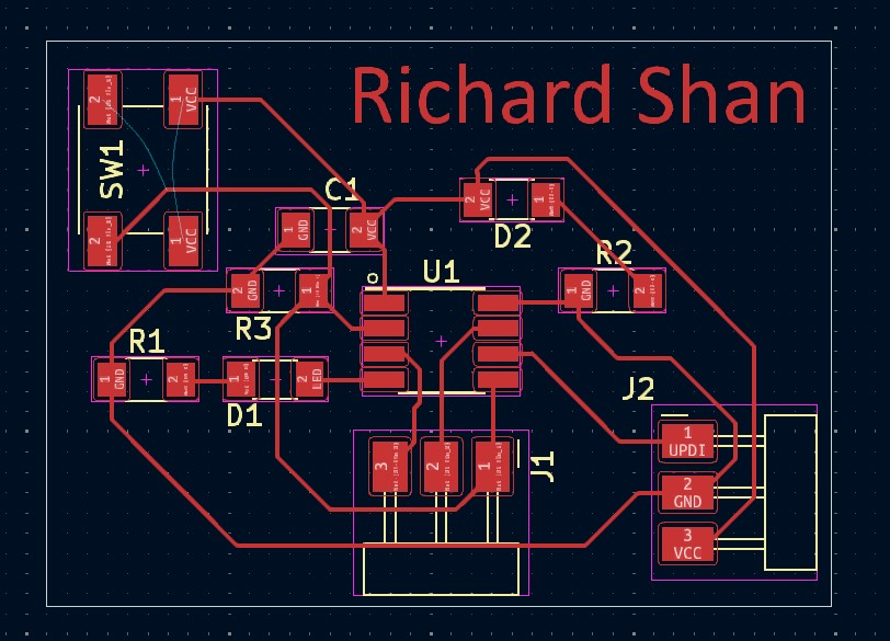
The board is now complete! I exported the files as GBR files and sent them to the milling machine!